
Abstract
Single micrometer-sized features were fabricated on ARN-4340 photoresist using a 3D additive technique of two-photon polymerization (TPP). An economic TPP setup capable of producing a large area was developed in the lab using a sub-nanosecond laser. The Photo-initiator (2, 4 Diethyl-9H-thioxanthen-9-one) with a large two-photon absorption cross-section was used to enhance the polymerization. It was theoretically determined that the dimensions of the polymerized features depend on the concentration of the photo-initiator. A novel image-based focusing technique was developed to achieve uniform microsized features on a large area. In the proposed TPP setup, the developed focusing technique was used to determine the area over the sample, which can be polymerized in one go. To demonstrate the capability of the developed setup, microstructures of about 1 µm width were fabricated over an area of 4 cm2. Further, the fabricated sample was used to develop a master mold of Polydimethylsiloxane, which can be used for a soft-lithography replication process. Also, the melt flow technique was explored to reduce the roughness in the fabricated structure. The multi-photon polymerization process using the sub-nanosecond laser is shown to be cost-effective and robust for large area microstructure fabrication.
Keywords
Introduction
Fabrication of nano and micron-scale features over a large area is required for various applications such as: metamaterial infrared absorber,1,2 biomedical applications,3,4 dielectric metamaterials for optical elements, 5 photonic crystals,6,7 and microfluidic devices,8,9 etc. Various techniques have been developed for the fabrication of micro-and nanostructures such as Focused Ion Beam (FIB),10,11 Electron Beam lithography (EBL),12–14 Laser Beam Machining (LBM),15–19 Interference Lithography,20,21 and Micro-lens array lithography using femtosecond laser.22–24 However, the above-mentioned techniques have their benefits and limitations. Techniques such as FIB and EBL provide very high feature resolution at a nanometric scale but are not scalable for rapid manufacturing over large areas because of the high machining time. LBM (single photon absorption) is a fast process that can be used for generating micrometric features. But large heat-affected zones (HAZ) associated with laser machining are not desirable while fabrication of high-resolution features. Micro-lens array is another technique that could be used for the fabrication of nanometer-size features provided the features have simple geometry. One other technique that could be used for high-resolution complicated features is TPP which is an additive manufacturing technique that gives high-resolution.
TPP has become an attractive method for the fabrication of complex 2-D and 3-D micro-structures with various types of materials and utilizes essentially the photochemistry initiated by two (or multi) photon absorption events.25,26 Typically, the very high laser intensities possible with focused femtosecond pulses can cause multi-photon absorption to occur in most organic materials.
27
Since the multi-photon absorption rate depends on the square of the laser intensity (
The equipment cost can be minimized using aQ-switched picosecond or sub-nanosecond laser instead of a femtosecond laser. However, for this photo-initiator molecules having large two-photon absorption cross-sections are needed to initiate the polymerization. The photo-initiators can reduce the operating intensities by several orders of magnitude when added in only small quantities due to their large multi-photon cross-sections. Several multi-photon absorbing materials have been reported to be used for multi-photon polymerization using picosecond and sub-nanosecond lasers. 28 Hybrid organic-inorganic resists SZ2080 (ORMOSIL) was specially created for TPP and was extensively used to fabricate high-resolution structures with picosecond lasers.29–31 Also, 2,4-diethyl-9H-thioxanthen-9-one was shown to effectively work as a photo-initiator with SZ2080 photoresist using 8 picosecond laser pulses. 32 These results paved the way for low-cost fabrication systems and moving toward rapid industrial production. 33 Kumar and Anantha Ramakrishna 34 developed a TPP setup using a sub-nanosecond laser to fabricate sub-micron 3D features on SU-8 photoresist and ARN-4340. In most of the available literature, the emphasis is on achieving a higher feature resolution, and the samples are fabricated only over an area of a few hundred square micrometers at the most. These features need to be manufactured or replicated for real-life applications such as photovoltaic devices or biomedical devices over large areas of several square centimeters to square meters.
One of the prime difficulties in fabricating large microstructures using TPP is the variation in the laser focal spot (LFS) on/inside the sample due to surface/thickness variation, such as the wedge angle of a substrate or even tilt caused by the mounting mechanisms. Due to the variations in the LFS, there are imperfections in the voxel dimensions. For large area structuring, the LFS has to be kept at the desired depth by refocusing constantly. Over the years, researchers have developed various autofocusing techniques, which mainly could be classified into two: optics-based autofocusing 35 and image-based autofocusing. 36 In an optics or hardware-based autofocusing system, a sensor that continually measures the distance between the lens and the sample is used to give input if there is a change in the distance, which may be caused by a variety of external sources such as vibrations, thermal drift, and so forth. 35 It has a rapid response and high focusing accuracy, and therefore it is widely used in the industry for automated optical inspection and machining applications with real-time requirements. However, high-end optics in the setup itself make this technique cumbersome and expensive to use. In image-based systems, autofocusing relies on the image sharpness identification or image spatial frequency function. Commonly available inexpensive cameras can take images, and post-processing can easily be carried out using image processing software. The software’s feedback was then used as input for various hardware to adjust the LFS during polymerization. With recent advances in computing through graphical processing units (GPUs) and other real-time processing technologies, very fast calculations can be performed. In our case, where the corrections for the depth need not be performed very rapidly, we had developed a MATLAB code to check whether the LFS is at the desired position or not. Given that all the hardware such as camera used for the focusing technique were already present in the setup, the proposed focusing technique is cost-effective, reliable, and robust.
In this article, we demonstrate a robust economic system that is capable of fabricating sub-micrometer scale features over large areas. The laser micro writer system of Kumar and Anantha Ramakrishna 34 was modified to make a large area of 2D laser writing using a novel focusing technique. Numerical simulations and experiments were carried out to quantify the effects of laser power and exposure time on the polymerization process. For focusing, it is noted that the laser beam had a reasonably large depth of focus (Rayleigh range) of a micrometer for writing micrometer-scale features. Therefore, the focus was not required to be continuously monitored and adjusted for slow substrate surface depth variations. Hence, an economic offline novel focusing system using an image correlation technique was developed, whereby, the laser writing is interrupted only after the beam transverse substantial distance to adjust the focus.
Consequently, we have shown that the developed setup can be used in two ways. It can either be directly used to fabricate required features on the polymer or for making a master mold to replicate the small micro-features over large areas in a short time by imprint lithography. Finally, it has been shown that the quality of of the replicated features can be improved using the polymer's melt flow technique.
Experimental setup
Figure 1 shows the photo and the schematic of the developed TPP system. A diode-pumped solid-state sub-nanosecond (700 picoseconds) laser (Wedge_ 532_1064, Bright Solutions, Italy) which is very economical as compared to normally used femtosecond lasers, simultaneously producing light both at 1064 nm wavelength (fundamental) and 532 nm wavelength (second harmonic), was used as the source. A dichroic mirror rejected the 1064 nm light and only the 532 nm beam was used for polymerization. The laser produces a coherent Gaussian beam (M2 = 1.3) and has a maximum pulse repetition rate of up to 100 kHz. A pinhole was placed in front of the laser to aperture the Gaussian beam. The laser beam was directed through an acoustic optic modulator (AOM – IntraAction Corp., USA) into an inverted microscope (Nikon Ecllipse, Japan) using dielectric coated high reflectance mirrors.
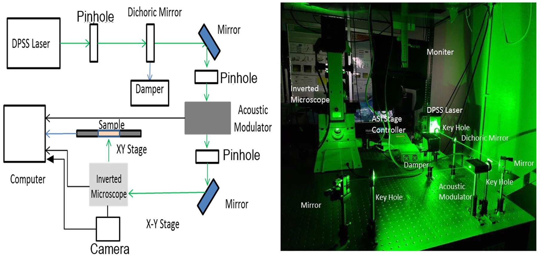
(a) Schematic showing the arrangement of various components use for developing the TPP setup, (b) image of the same TPP setup.
The AOM was aligned at the Bragg angle to diffract the beam into three diffracted components (+1, 0, −1) for use as a switch. The +1 mode alone was coupled to the microscope. The beam then passes through a high NA objective lens for focusing before interacting with the polymeric medium. The use of different NA objective lenses results in differing feature resolutions. The sample was placed on a stepper motorized XY stage (Applied Scientific Instrumentation, MS-2000 Flat top XY stage) with a 120 mm × 75 mm travel length and a closed-loop movement resolution of 250 nm. The real-time polymerization and writing by the laser were monitored in reflection mode by a Nikon camera coupled through a dichroic mirror that rejects the green light at a side-port of the microscope. The same camera was also for the initial focusing of the sample and to monitor the polymerization process.
The movement of the stage and AOM were controlled using a LabVIEW (National Instruments) program such that the (+1) component of the beam comes when the stage moves. The program could easily be modified to reverse the combination between AOM and stage. The program was also used to provide linear movement to the stage by giving coordinates in a text file. The sample was kept inverted on the stage so that the beam faces the photo resin directly. The beam was focused at the interface of the glass substrate and coated photo resin. To verify the developed laser writing technique and to check the closed-loop accuracy, we initially fabricated various shapes and sizes: from a single straight line to a circle. It was observed that the starting and endpoint for all the features were the same, which shows the good fidelity and reproducibility of the writing by the setup.
Numerical formulation
Zhou et al., 37 in their review article, gave a formulation for the numerical study of TPP using a femtosecond laser. Using this formulation, we studied the TPP writing by a sub-nanosecond laser.
Determination of voxel dimension
TPP is a photochemical process initiated by the laser beam tightly focused on the photosensitive resin volume by a high numerical aperture (NA) objective. Photopolymerization consists of three processes: the initiation process, the propagation process, and the termination process. In the initiation process, photo-initiators (PIs) reach the excited state (PI*) by absorption of two photons and decompose to radicals (R·). In the propagation process, the radicals combine with monomers (M) to produce monomer radicals (RMn ·). In the termination process, two monomer radicals are combined, and the photopolymerization process terminates. Photopolymerization is described in the following equation. 37

The density of radicals which are produced by the laser pulses, as shown in the above equation, can be predicted by using a simple rate equation 37 :
and the solution can be expressed as:

where, σ2 is the effective two-photon cross-section for the generation of radicals,
where, P is the average power, t is the total processing-irradiation time,
where,
Using these parameters, the variation of voxel width with time for different values of
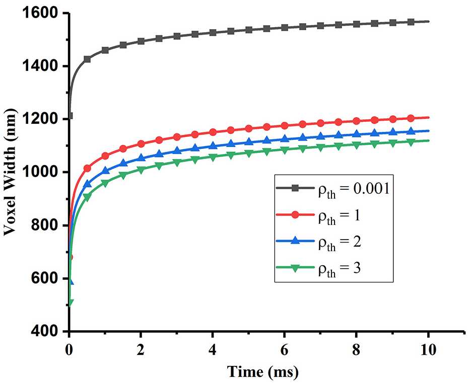
Variation of the voxel width with time for different values threshold photo-initiator (
Determination of
th
As discussed above, for the calculation of voxel dimensions, we need
Focusing technique
The polymerization in TPP takes place within the resin at the LFS (laser focal spot). For fabrication, LFS initially maintained at the interface of the glass substrate and the resin. After developing the resin, the polymerized part should remain intact with the glass. LFS was moved in the desired direction within the resin to achieve the final polymerized product. However, if the resin thickness is minimal, like for 2D writing, the slight wedge angle in the substrate leads the LFS to move outside the resin. Wedge angles up to milliradian are present in most of the samples because of many possibilities such as tilt in the stage, deviation in glass substrate or uneven coating of photoresist. Figure 3 shows an exaggerated view of the wedge angle (θ).
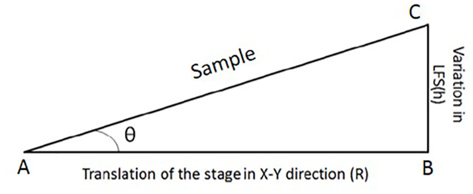
Variation in the sample height with the wedge angle.
Let us suppose, the laser is focused at point A on the sample and there is a requirement of polymerizing the sample from A to C. Ideally, the sample should move in a plane A to B and “θ” should be zero, however, in actual practice the presence of “θ” cause the sample to move in a different plane as shown in the Figure 3. Given that the LFS remains in the same plane, the sample after a certain variation moves out of focus. The vertical variation between the sample and the LFS could be neglected if it is within the depth of focus of the laser beam, which is given as:

where zR is the Rayleigh range of the laser beam. Rayleigh range is the distance along the direction of propagation of the beam from the waist to the place where the cross-sectional area is doubled and can be calculated using the following equation:
where
where f is the focal length of the lens and a is the aperture diameter. The specifications for the objective that we used (Nikon TU Plan Fluor 50X) are, a = 1.25 mm and f = 1 mm. Substituting these values in the above equations, we get the depth of focus = 8.557 μm. Therefore, if the variation in the sample is more than 8.557 μm, then the polymerization will deteriorate that is, the polymerized height is less than 100 nm. To avoid such problems, there is a need to continually readjust the distance between the sample and the lens such that the beam focus remains within the depth of focus.
Focusing methodology
As discussed in section 1, all the existing solutions for the autofocusing of TPP are either very expensive or highly complex to use. Therefore, we had developed a novel focusing technique that is cost-effective, maintenance-free, and straightforward setup for focusing by using MATLAB software and Nikon camera. The developed focusing technique consists of a MATLAB code that uses the normalized correlation function.39,40 The normalized correlation function gives a correlation value that varies from 0 to 1 between two images, where 0 stands for no correlation, and 1 stands for complete correlation between the images. In our case, one of two images to be correlated was taken at the start of polymerization (baseline image) and the other at any instance during polymerization (target image). Therefore, the correlation coefficient gives the similarity between the baseline image and the target image.
The MATLAB program used the pixel intensity over the array of 640 × 480 pixels to distinguish between the polymerized and unpolymerized areas. Experimentally, we observed that in an image the crosslinked parts had pixel values less than 148 and unpolymerized/non-cross-linked areas had values higher than 148. Using this knowledge, image binarization was carried out. Binarization was done by assigning pixel values of 255 (representing white) to pixels having an intensity above 148 and 0 (representing black) to all the remaining areas. After binarization, the codes run in 1.5 s which is 40% less than the previous time. After binarization of all the images, they were correlated with the baseline image to obtain the correlation values. Figure 4 shows the converted camera image of a polymerized line into a binary image. In the binary image, the polymerized parts are marked white while the rest is black.
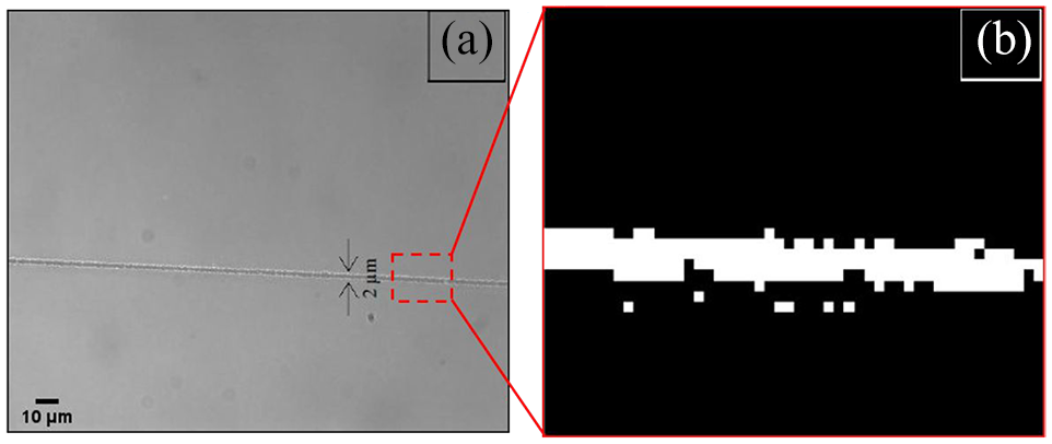
Image of the sample consisting of a polymerized and unpolymerized line: (a) camera image and (b) enlarged view of the section of the captured image after binarization.
Furthermore, to validate the used focusing technique, experiments were conducted. In the experiments, the microscope was initially focused manually, and the fabrication process was initiated. The image was captured at the focused region, which was considered as the baseline image. All the other images which were captured at other instances during polymerization were correlated with the baseline image. Figure 5 gives the 3D and 2D view of the correlation graph of the images taken at the start of polymerization and any instant during polymerization with the baseline image using the above-mentioned correlation technique. As can be seen in Figure 5, the correlation value is 1 for the images at the same focal plane which validate the used technique and it decreases as the samples move away from the starting point (focused region). It shows that the quality of the polymerization does not remain the same throughout the polymerization. Therefore, it becomes imperative to know the correlation value beyond which the focus need to be adjusted.
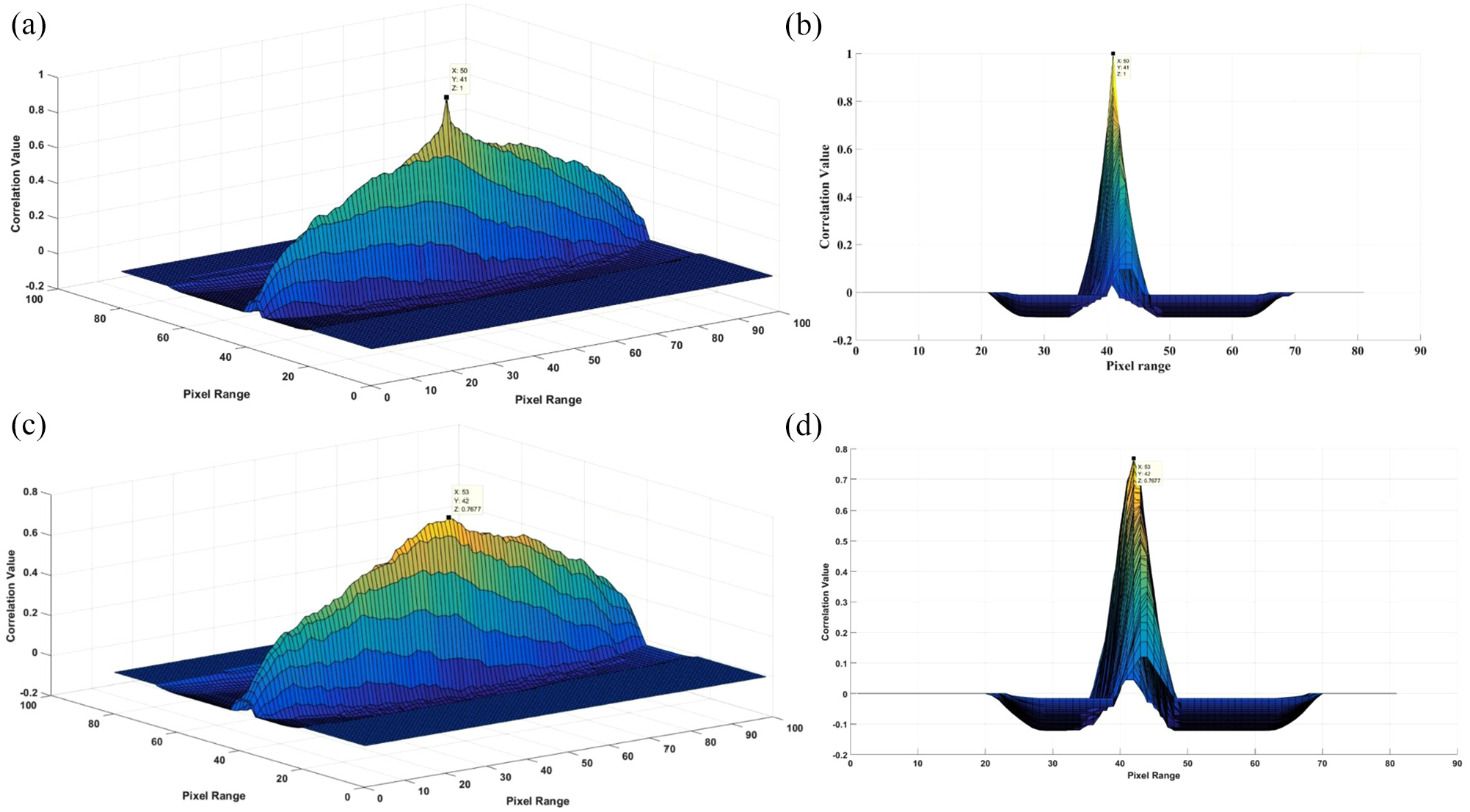
Correlation values of the images 100 × 100 pixels in X-Y direction taken at (a and b) start of polymerization (c and d) during polymerization.
Threshold correlation value
As discussed earlier, the voxel characteristics will not deteriorate as long as the sample is within the depth of focus. To realize the threshold correlation value up to which the voxel characteristics do not deteriorate, polymerization was carried out at a variable vertical distance from the focus with a step size of 1 μm. Atomic force microscopy of all the polymerized samples was carried out, and the obtained AFM data for every sample was associated with their corresponding calculated correlation value. In the experiments, it was found that up to the correlation value of 0.6, there was less than 10% variation in the voxel characteristics. Below this value, the voxel characteristics start deteriorating, and hence the threshold correlation value was fixed to be 0.6.
Further, Figure 6 shows the correlation values between the polymerized area at a different distance from the focal plane. As can be seen in Figure 6, a total of 10 points are above the threshold value that is, 0.6 and each point depicts a variation of 1 μm from the neighboring point. Excluding the focus point, which was at zero, 9 points are above the threshold correlation value. Hence, the total absolute distance that is, in positive and negative Z-direction that can be allowed so that the correlation value is within the threshold value (0.6) is 9 μm, which corresponds to the depth of focus for the TPP setup, which was calculated to be 8.557 µm. This shows that this technique has a percentage accuracy of 95%.
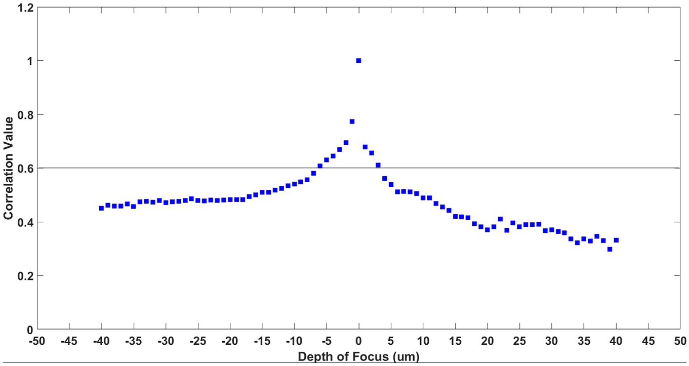
Correlation value of all images taken up to the distance of ±40 μm from the focused plane with the step size of 1 μm with the image at focus (baseline image).
Results and discussion
Parametric optimization
A parametric study was carried out to optimize the process parameters: laser power and writing speed, for the fabrication of the desired dimensions on the prepared ARN photo resin. For ARN photo resin preparation, 3% w/v of photo-initiator was added to the ARN photoresist. It was then spin-coated at 2000 rpm for 1 min on a glass slide. After coating, for hardening, the sample was kept at 85° C for 2 min in an oven. In this study, the laser power was varied from 10 to 24 mW, and writing speed was varied from 0.5 to 1 mm/s. The effect of these parameters on writing speed and laser power are discussed in the following sub-sections.
Effect of writing speed
The writing speed needs to be optimized to achieve the desired features in the minimum possible time. Figure 7 shows the effect of writing speed on polymerized width and height at 18 mW laser power and 20 kHz frequency. As shown in Figure 7, the obtained cross-polymerized region’s width and height decrease with an increase in the writing speed. It is due to the reduction in the interaction time between the substrate and the laser beam as the writing speed increases. This leads to the decrease in energy transferred from the laser beam to the substrate due to which there is a decrease in the number of monomers that will be crosslinked.
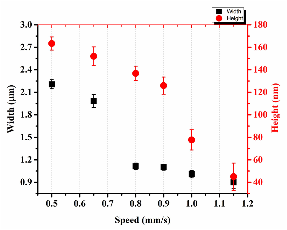
Variation in the width and height of the polymerized spot with writing speed.
Effect of laser power
Figure 8 shows the effect of the laser power on the polymerized features’ width and height at 0.8 mm/s writing speed and 20 kHz frequency. As shown in Figure 8, with an increase in the laser power, the obtained polymerized width and height increase up to 21 mW, because with an increase in the laser power, more energy will be imparted to the substrate, which leads to more crosslinking of the monomers of the photo resin in both directions. However, with a further increase in the laser power instead of the polymerization, ablation sets in the substrate. It is because the laser beam increases the temperature of the substrate, hence, higher laser power beam will lead to higher temperature of the photo resin. If the laser beam has sufficient energy to increase the temperature of the sample beyond the melting and vaporization temperature, it will ablate the sample.
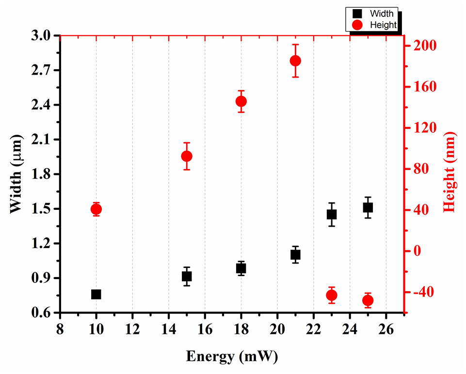
Variation in the width and height of the polymerized spot with laser power.
As can be noticed from the above discussion, both laser power and writing speed are related to each other as an increase in the laser power will increase the energy transferred to the photoresist. The increase in the writing speed will decrease the energy transfer to the photoresist. So, there could be better understanding of polymerization process parameters in terms of exposure time. Exposure time is the time for which a particular spot is exposed to the laser beam. For higher laser powers, the exposure time should reduce while for the lower laser powers, the exposure time should increase for achieving the desired output. This is while assuming that the laser pulse peak intensities are large enough to cause two-photon absorption effectively.
Figure 9(a) shows the polymerized image for a shorter exposure time that is, at a laser power of 16 mW and writing speed of 1 mm/s. As can be seen, the obtained polymerized height is about 30 nm which is very small for most applications. Figure 9(b) shows the polymerized image of the sample when the exposure time was increased by increasing the laser power and decreasing the writing speed. The values used were: 21 mW and 0.8 mm/s for laser power and writing speed respectively. As can be seen in Figure 9(b), we obtained a sufficient height of about 200 nm and the desired width of around a single micron. When the exposure time was further increased by increasing the laser power to 23 mW and keeping the writing speed the same at 0.8 mm/s, ablation was seen instead of polymerization as shown in Figure 9(c).
AFM images of line fabricated at: (a) higher, (b) optimized, and (c) higher exposure time.
Experimentally, for obtaining the single micron features, the optimized parameters were found to be 21 mW power, 0.8 mm/s writing speed, and 20 kHz repetition rate. These experimental results were compared with numerically obtained voxel dimensions using the equations (6) and (7). All parameters except ρo = 3% w/v and ρth = 0.1% w/v were kept same as before. Using these parameters, the obtained voxel length and diameter are shown in Figure 10. It can be seen that at the above parameters, the calculated voxel width was also around 1 µm and voxel length was around 4 µm.
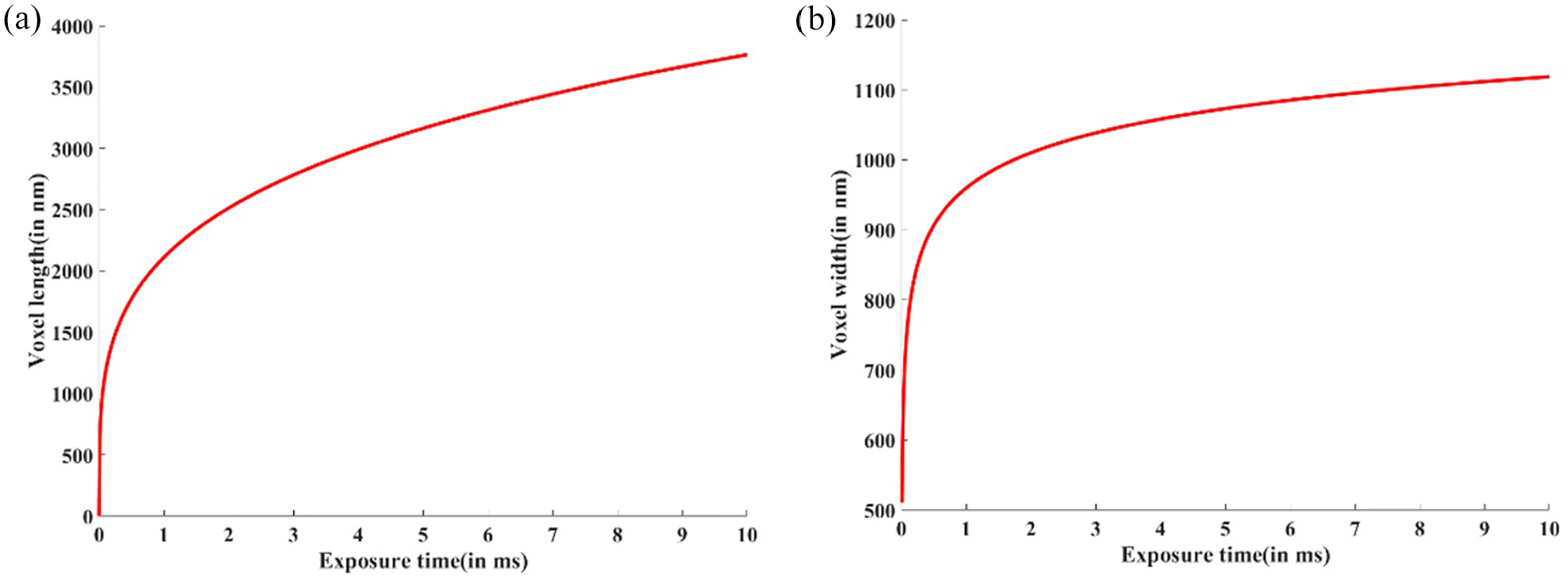
Variation in voxel dimension with exposure time: (a) length and (b) width at the optimized parameters using the analytical data.
Large-area fabrication
A resin of ARN-4340 photoresist was prepared by mixing it with 3% w/v of 2, 4 Diethyl-9H-thioxanten-9-one, and then spin-coated over a glass substrate of 2.5 cm × 2.5 cm at 2000 rpm. It was then heated for 2 min at 85°C in an oven. The sample was kept for some time to bring it down to room temperature. The obtained thickness of the photo resin on glass was expected to be 2 µm. As discussed in section 4, the sample needs to be refocused for proper polymerization after a certain length. Therefore, before starting the final polymerization over large areas, we first determined the travel distance, which in our case was found to be about 2.5 mm (i.e. when the correlation value is more than 0.6) after which we had to refocus the sample. Therefore, patches of
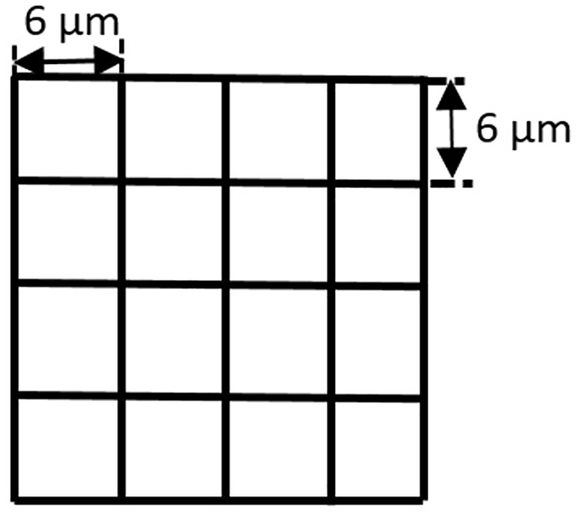
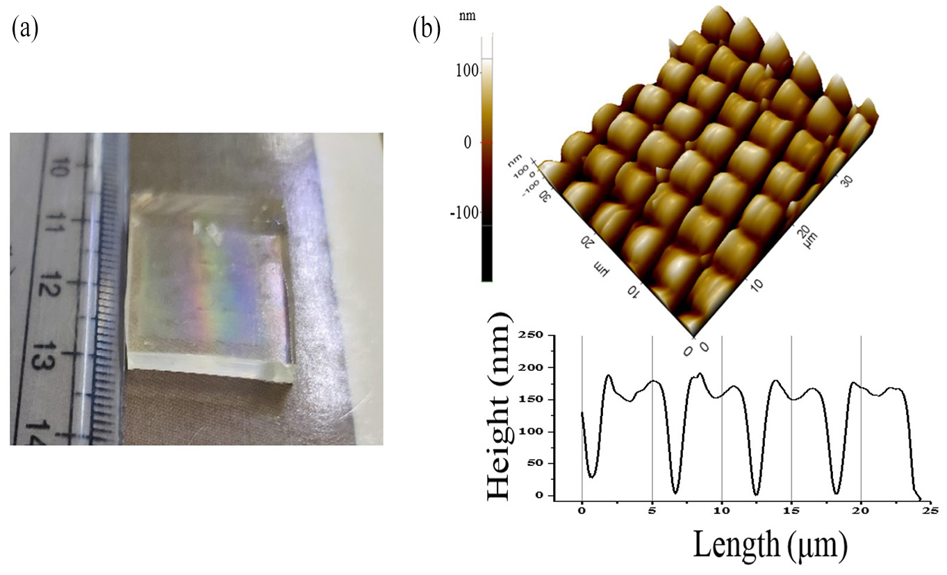
Schematic of the mesh type structure which was fabricated using TPP. This mesh structure is polymerized over an area of 4 cm2.
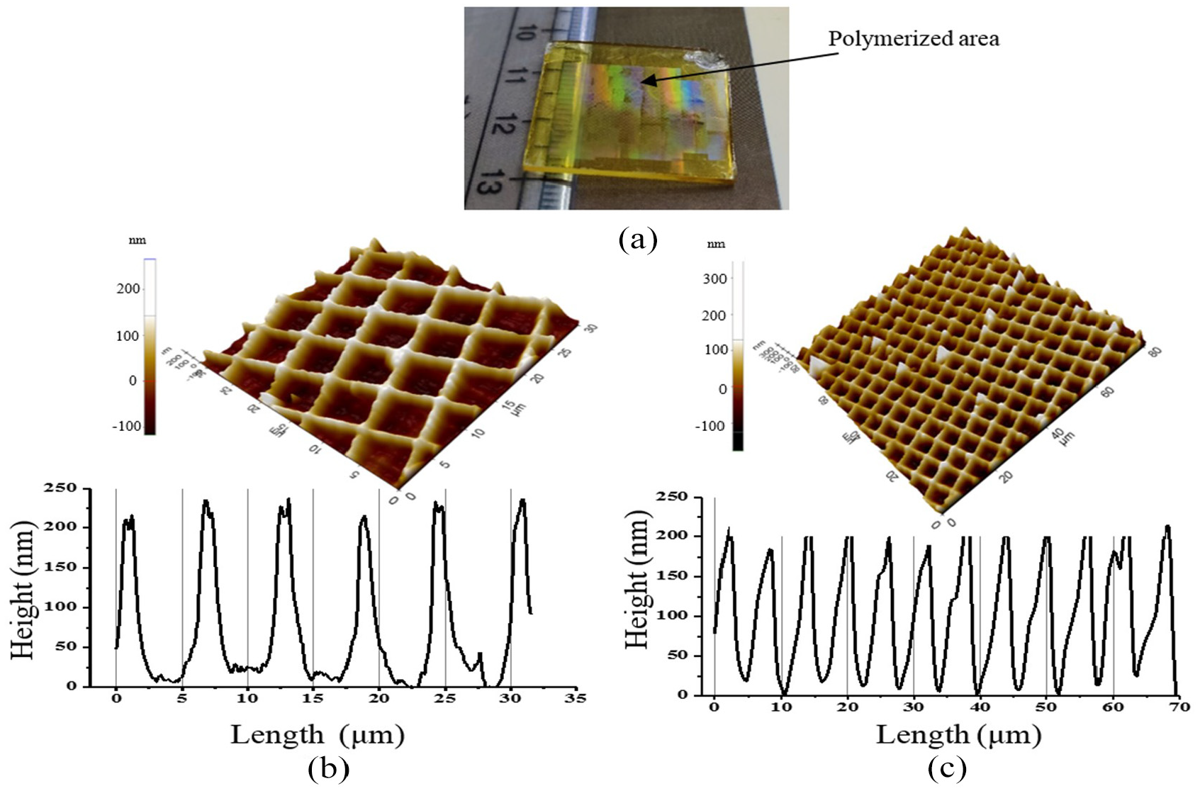
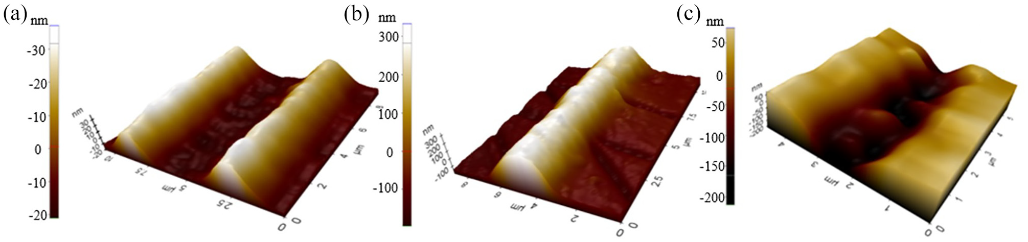
(a) Image of the fabricated sample using TPP the reflection from the sample shows the presence of micro structures(b and c) AFM images of the fabricated sample at various locations.
Master mold fabrication
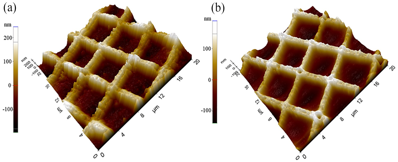
The fabricated structures can be directly used in the applications such as infrared metamaterial absorbers and can be used to make the master mold for imprint lithography. For the master mold fabrication, the polymerized sample was initially kept in a petri dish. Then silicone elastomer (PDMS) was poured over it. PDMS (Syigard 84) is a non-toxic material and has excellent transparency in the UV to an optical range of wavelengths. The sample was then vacuumed to remove the air bubbles, after which it was kept in an oven at 65°C for 6 h to get hardened. When the sample was cooled to room temperature, silicone elastomer was peeled off from the polymerized sample. Figure 13(a) shows the fabricated master mold on PDMS from the polymerized sample and the fidelity of the transfer of the features. The reflection on the top surface of the PDMS shows the micrometer features’ presence, and Figure 13(b) shows the AFM images taken in the non-contact mode at various polymerized areas.
Silicone elastomer master mold made from fabricated sample: (a) image of the fabricated master mold in which presence of micro pillars can be felt by reflection and (b) AFM image of a random area of the master mold.
Melt flow of polymer
Imprint lithography is a well-known technique for the fabrication of large-area samples, which used the master mold to transfer desired features on the sample. This master mold could also be used repeatedly for the fabrication of structures as desired for various applications over a large area, as shown by Kumar et al. 2 They had fabricated a disk array on the photoresist coated on a polished silicon substrate using laser interference lithography. They had used the fabricated sample as a master for replicating the features on the other surface using soft lithography. Initially, they had fabricated an elastomeric stamp of PDMS using the master sample. Using the stamp, the features were transferred to the other surfaces repeatedly, and a microwave infrared absorber of 8 cm × 10 cm was obtained. In our case, large area MIR can be realized directly by fabricating inverse structures using the developed TPP setup. Thus, it is an advancement over the setup of Kumar et al. 2 In our case, the structured large-area master mold can also be used to transfer the structures to another surface using soft lithography in a manner much more quickly than in Kumar et al. 2 due to the large areas involved here. We had also fabricated the parent structure on a commercially available photoresist (NOA 61) using the aforementioned silicone elastomer mold. Figure 14 shows the AFM images of the features transferred on the photoresist.
Variation in the roughness of the structure made on UV curable polymer using fabricated silicone master mold:(a) before melt flow and (b) after melt flow.
As it can be seen in Figure 14(a), the roughness of obtained features on photoresist is high, which is not desirable. This roughness can be reduced using the melt flow technique. In this technique, the sample is heated at a high temperature so that the material accumulated in the form of peaks gets melted and smoothens out due to the surface tension. We had heated the whole structure at 120°C for 3 min. Figure 14(b) shows the obtained structures after melt flow. As can be seen, there is a significant reduction in the roughness after melt flow. However, the parameters such as the heating temperature and time can be further optimized for achieving lower roughness of the final features. It can be done by conducting experiments for optimizing the heating time and temperature.
Conclusions
To realize the large-area fabrication of nano and microscale features, we have developed a TPP setup with a novel-focusing arrangement for locating the laser focus spot within a prescribed distance of the substrate’s surface. The setup is equipped with an AOM to control the beam exposure and a linear stage for the LabVIEW program’s sample movement. The TPP setup could be used to fabricate microfeatures of about 1 µm over areas as large as required in a single operation. An offline novel focusing technique based on image correlations was developed in MATLAB for refocusing the laser beam at the sample surface. The depth of focus can change due to various factors, including the substrate’s wedge angle, inhomogeneous resin deposition, mountings, etc. It was observed that up to a correlation value of ∼0.6, there was no need to refocus the laser beam. From the analytical study, it was observed that the value of
Footnotes
Acknowledgements
We would like to thanks Dr. Vyom Sharma, Department of Mechanical Engineering, IIT Kanpur for his help in editing and Mr. Hrithik Das (20163141), Department of Mechanical Engineering, Motilal Nehru National Institute of Technology for his help in this work.
Declaration of conflicting interests
The author(s) declared no potential conflicts of interest with respect to the research, authorship, and/or publication of this article.
Funding
The author(s) received no financial support for the research, authorship, and/or publication of this article.