
Abstract
In electrical discharge machining, the rapid heating and quenching effects cause the formation of resolidified layers, heat-affected zones, and defects, which have a tremendous impact on the mechanical properties of materials. Thus, to analyze the formation and evolution process of defect structures, single discharges in polycrystalline copper were simulated. The research results show that after a discharge, a larger number of stacking faults and dislocations existed in polycrystalline copper, which were mainly concentrated under the discharge crater and bulge. In these defects, the bedded stacking faults played a dominant role. Additionally, the results indicate that under the same discharge conditions, the diameter of the discharge crater in polycrystalline copper was larger than that in monocrystalline copper, whereas their depths were almost the same, and the volumes of both the bulge and removal debris generated in polycrystalline copper were larger than those generated in monocrystalline copper.
Keywords
Introduction
Due to the unique and superior properties of using thermal energy to machine electrically conductive materials regardless of hardness, electrical discharge machining (EDM) has become a widely used technique in the manufacturing of complex-shaped dies, molds, and critical parts in the automobile, aerospace, surgical industries, and so on. This technique has also been successfully applied in the micro-manufacturing fields, such as microelectromechanical system (MEMS), micro-holes, and micro-molds, and even in the nano manufacturing fields. 1 However, although EDM technology has made enormous progress and the performance of EDM has been greatly improved, the nature of many phenomena and mechanisms behind EDM has not been extensively theoretically studied. This is because EDM occurs randomly in a very short time and in a very narrow space, making both theoretical and experimental studies extremely difficult. 2 To gain insight into these fundamental issues and understand the detailed mechanisms and phenomena associated with EDM, many researchers utilized computational simulations, which can overcome the theoretical and experimental shortcomings. For instance, Assarzadeh and Ghoreishi 3 used the electrothermal-based finite element simulation model including a Gaussian-type distribution of the spark heat flux, temperature-dependent materials properties, the latent heat of melting, and expanding plasma channel with a pulse current and time to simulate the mechanism of crater formation. Izquierdo et al. 4 produced a numerical model of the EDM process considering the effect of multiple discharges to efficiently predict the surface roughness. Liu and Guo 5 presented a numerical approach to simulate the massive random discharges on the machined surface. However, in those finite element method (FEM) models, only the heat transfer of the material was considered and not the dynamics behavior, which made it difficult for those models to reveal the natures of the mechanisms and phenomena in EDM, such as the material removal mechanism and motivity, and the formation and evolution process of defects generated during the discharge process. Thus, FEM considering only the heat transfer is not preferred.
Molecular dynamics (MD) simulations have been used extensively during the past few decades to investigate the physical movements of atoms and molecules and gained popularity in the materials, physics, chemistry, biology, and even in the machining and manufacturing fields. In recent years, because of the superior advantages in the research of the mechanical and thermal behaviors of materials, MD simulation of the EDM process has also attracted researchers’ attentions. For example, Yang et al.6,7 first realized the MD simulation of a single-discharge process. A series of MD simulation results and phenomena associated with EDM were successfully obtained such as the material removal process, the distribution of the removed material in the gap, and the stress distribution. Moreover, Yang et al. 8 initially tried to explain the material removal mechanism and motivity using MD simulation. Yue and Yang 9 clarified the detailed formation process of the bubble and analyzed its function and influence on the material removal process of EDM. However, in practical applications, most materials are polycrystalline, while those simulations mainly aimed at monocrystalline materials and did not consider the polycrystalline materials whose mechanical properties are different from the monocrystalline materials.
Therefore, to investigate the machining properties of the polycrystalline materials, we performed a MD simulation of the material removal process of a single discharge in polycrystalline copper. Based on the simulations, the material removal process in polycrystalline copper was analyzed using the centro-symmetry parameter (CSP) method. Then, the resolidified layer, the heat-affected zones (HAZs), and the crystal defects generated in polycrystalline copper were analyzed. Finally, the influence of the crystal structures of polycrystalline and monocrystalline copper on the machining process is discussed.
Modeling and computational details
MD model of EDM
The simulation was carried out using a large-scale atomic/molecular massively parallel simulator (LAMMPS). In Figure 1, the simulation model is 50a (where a is the lattice constant of copper and equals 3.615 Å) thick (along the Z direction) and 76a wide and long (along X and Y directions), in which two different crystal structures (monocrystalline copper and polycrystalline copper) were built as shown by Figure 1(a) and (b), respectively. In particular, polycrystalline copper contained 92 randomly orientated grains, which was built based on the Voronoi diagram. The detailed process of material modeling of the polycrystalline copper is presented in Appendix 1. To prevent the simulation model from unexpected movements, boundary atoms were applied at the bottom of the electrode, and the thickness of the boundary atoms layer was approximately 2.5a. Additionally, thermostat atoms were distributed around the Newtonian atoms to ensure adequate heat conduction in the system, and the thickness of the thermostat atoms layer was approximately 1.5a. The other atoms were Newtonian atoms that followed Newton’s laws. The initial temperature of the model was set to 300K. The discharge was ignited on the top surface of the model. Considering that in actual EDM, the working gap is mostly occupied by bubbles even though the working gap is submerged in dielectric liquid, 10 the working gap was assumed to be a vacuum for simplicity.
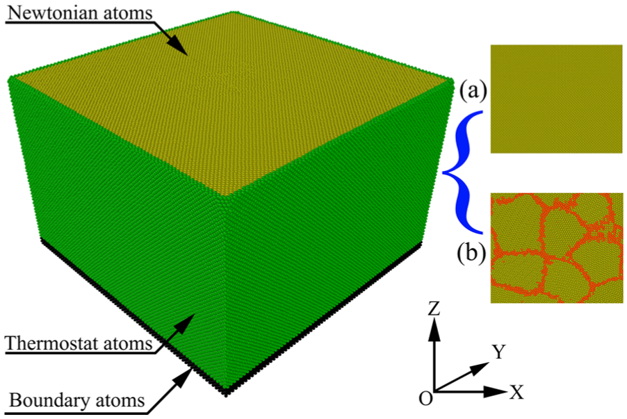
MD simulation model: (a) monocrystalline and (b) polycrystalline copper.
Interatomic forces
A three-body embedded-atom method (EAM) potential, 11 which is extensively used in the MD simulation of the interaction between copper atoms, was used in this simulation. For the EAM potential, the total atomic potential energy of system Etot can be expressed by the following equation
where
Heat source model
In actual EDM, an arc column whose diameter is changing with time is formed by a discharge and consists of plasma made up of ions, electrons, and neutral atoms. To simplify the simulation process, the forming and expanding process of the arc column was not considered, and the plasma particles in the arc column were also ignored. Thus, the arc column can be simplified as a Gaussian heat source with the constant diameter shown in Figure 2 and equation (3)

where r is the radial distance from the center of the heat source, q(r) is the heat flux at radius r, qm is the maximum heat flux at the center of the heat source, and k is the heat source concentration factor.
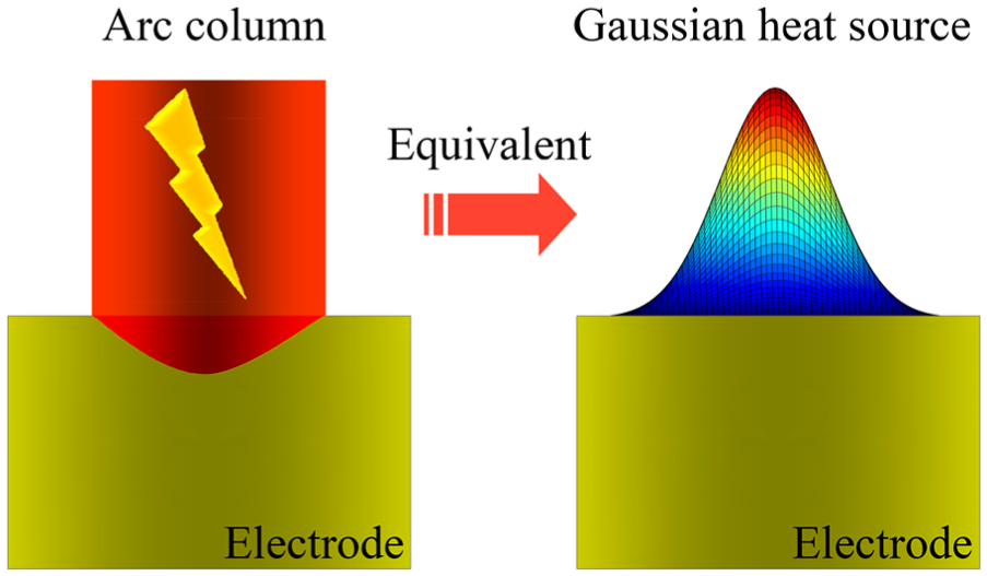
Schematic diagram of Gaussian heat source with constant diameter.
In the MD simulation, the energy from the heat source is added to the system of atoms by adding nontranslational kinetic energy to a group of atoms in a manner that conserves their aggregate momentum. Thus, in the system of atoms, the above Gaussian heat source can be expressed by equation (4) as

where rn is the radial distance from the center of the heat source for the nth atom, Pm is the heat flux at the center of the heat source in the system of atoms, and P(rn) is the heat flux at radius rn for the nth atom. The total computation and discharge times were 1.5 and 1 ns, respectively. The diameter of the discharge column and the maximum heat flux density at the center of the arc column Pm were 200 Å and 0.12 GeV/ps, respectively.
Heat addition into the system of atoms is performed every n time steps in the simulation, which is achieved by the fix heat command in LAMMPS. 12 Thus, in every n time steps, the heat energy applied to an atom is shown as follows

where Δt is n time steps in the simulation and E(rn) is the applied heat energy of the nth atom at radius rn.
Finally, the above energy from the heat source E(rn) is converted into the kinetic energy of the nth atom, ΔEk(rn), as shown in equation (6), by which the temperature of atoms can be calculated

where ΔEk(rn) is the increment of the kinetic energy of the nth atom at radius rn.
Identification of defect structures
In this article, we used the visualization technique of CSP 13 to analyze the resolidified layers and HAZs as well as the crystal defects. The CSP, which can describe the local disorder, is defined for each atom as
where the N nearest neighbors are identified and Ri and Ri+N/2 are vectors from the central atom to a particular pair of nearest neighbors. N is an input parameter. For the face-centered cubic (FCC) lattice, N is set to 12. For an atom on a lattice site, surrounded by atoms on a perfect lattice, the CSP is 0. Additionally, this parameter is near 0 for small thermal perturbations of a perfect lattice. If a point defect exists, the symmetry is broken, and the parameter has a larger positive value. Thus, we can use the CSP of an atom to identify the local disorder of one atom and the type of the crystal defects. In this article, the atoms are colored according to the value of the CSP with red for dislocations, green for stacking faults (SFs), and yellow for surface atoms based on the reference values in Kelchner et al. 13
Material removal process in a single discharge
Figure 3 shows the material removal process with discharge in polycrystalline copper. The CSPs of the materials before (t = 0 ps) and after discharge (0 < t < 1000 ps) were computed to clearly show the crystal defects inside the electrode. The results indicate that before the discharge (t = 0 ps), the polycrystalline copper consisted of many crystalline grains with different shapes and sizes. Among the crystalline grains were grain boundaries with imperfect FCC structures (CSP > 3), which were colored in orange. Inside the crystalline grain, the atoms have perfect or near-perfect FCC structures (CSP < 3).
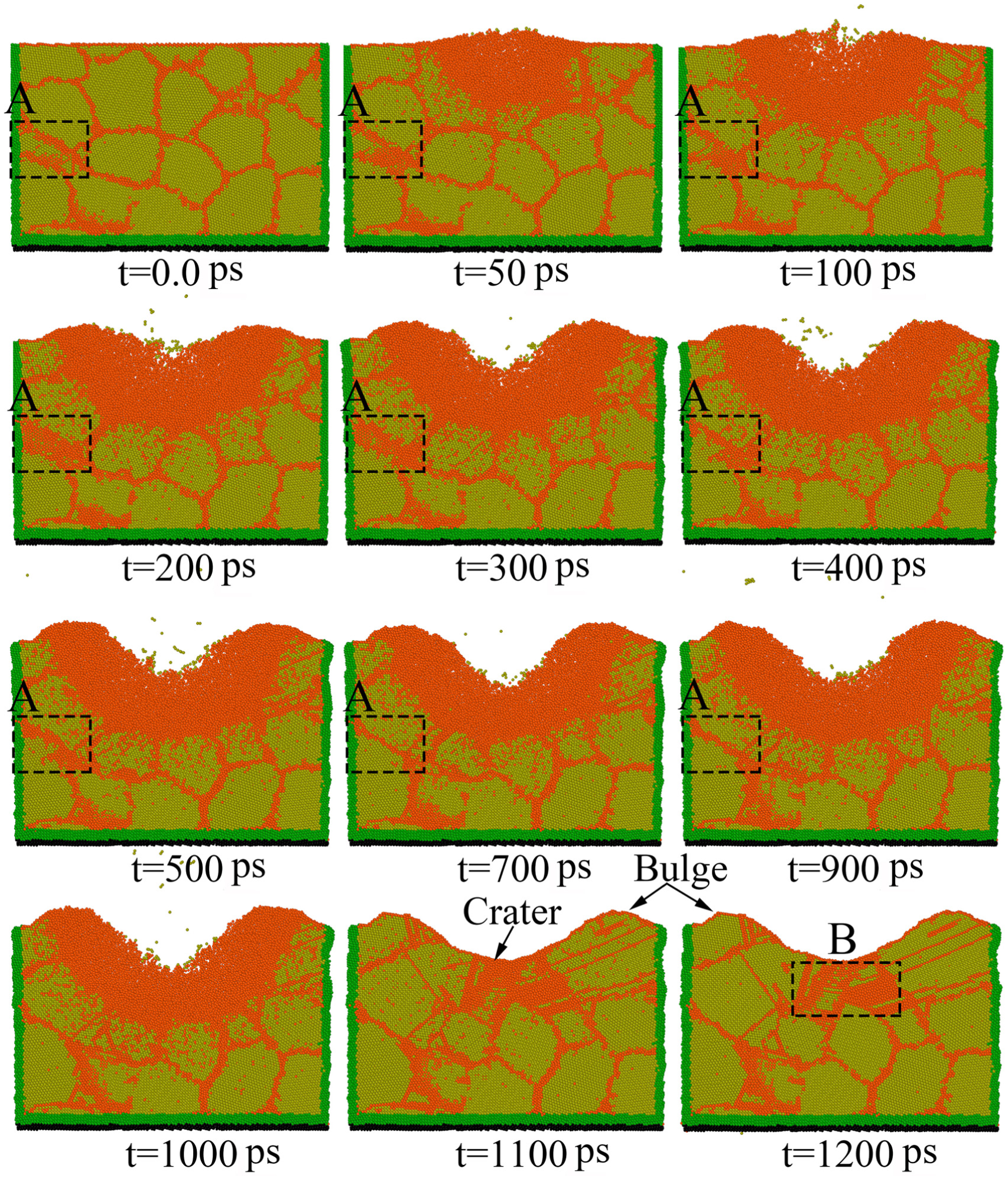
Middle sectional view of material removal process with discharge in polycrystalline copper.
After the discharge was ignited (0 < t < 1000 ps), the electrode material was heated by the extremely high heat flux from the discharge column. As a result, increasingly more atoms gradually deviated from their previous equilibrium positions due to the increase in atomic thermal motion. Thus, around the discharge spot at t = 50 ps, many crystalline grains, whose perfect FCC structures were destroyed, were mixed together, and their grain boundaries were vague and disappeared. But, at this time, there was no removal of material. As the discharge progressed and the material continued to be heated by the high temperature of the discharge column, the range of atoms with higher CSPs expanded gradually as shown at 100 ps. When the temperature rose over the melting point or vaporizing point, the material was melted and vaporized, and at this point, the material removal process began. During this period (200–1000 ps), a discharge crater was formed, and the bulge around the discharge crater was generated through the horizontal shear flow of the molten material. During the discharge process, the continuous heat input through the discharge was also transferred into the interior of the electrode material, which led to a change in the arrangement of atoms inside the electrode material. Then, we chose one of the changes inside the electrode to show the above phenomenon. As shown in this figure, the material in region A, far away from the discharge spot, did not melt, but the arrangement of atoms in this region obviously changed. Therefore, this region can be thought as a part of the HAZ in EDM.
After the end of the discharge (t > 1000 ps), the material cooled gradually, and the molten material recrystallized into a crystalline state. Compared with the crystal structures before the discharge, the atoms with imperfect FCC structures such as region B obviously increased, indicating that there were many crystal defects generated in the discharge process. Next, we analyzed the crystal defects generated during the EDM process.
The discharge process in monocrystalline copper, as shown in Figure 4, was also simulated using the same discharge conditions. The CSPs of the material before (t = 0 ps) and after the discharge (0 < t < 1000 ps) were also computed to clearly show the crystal defects inside the electrode, and the atoms with imperfect FCC structures (CSP > 3) were also colored in orange. From this figure, overall, the material removal process in monocrystalline copper was similar to that in polycrystalline copper. After the discharge was ignited (t > 0 ps), heated by the extremely high heat flux from the discharge column, the arrangement of atoms around the discharge spot was also destroyed, resulting in a large number of atoms with higher CSPs. The formation process of the crater and bulge in monocrystalline copper was the same as that in polycrystalline copper, as shown in Figure 3. However, there were still some differences between them. For the discharge in monocrystalline copper, the region of atoms with imperfect FCC structures was much smaller than that in polycrystalline copper. Moreover, compared with the polycrystalline copper, the effect of the thermal energy on the change in the arrangement of atoms in monocrystalline copper was much less, which indicates that the thickness of the white layer generated in monocrystalline copper is thinner than that in polycrystalline copper. In the next section, we analyzed their differences in detail and the effect of those differences on their material removal processes.
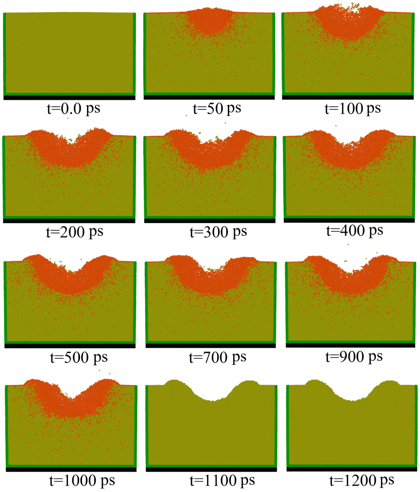
Middle sectional view of material removal process with discharge in monocrystalline copper.
Analysis of crystal defects in polycrystalline material
From the above analysis in Figures 3 and 4, in both polycrystalline copper and monocrystalline copper, during the EDM process, a large quantity of molten material was not fully removed but instead solidified on the discharge surface and formed a resolidified layer around the discharge crater, which was investigated by experiments.14,15 Additionally, the findings indicate that HAZs exist under the discharge crater. Thus, rapid heating and quenching process during EDM process, including the resolidified layer and the HAZ, have a tremendous impact on the mechanical properties of the material, such as the wear resistance, fatigue strength, hardness, and corrosion resistance. Thus, we analyzed the crystal defects inside the electrode.
Figure 5(a) and (b) shows the crystal defects after discharge (a) and before discharge, respectively. From Figure 5(a), it was found that after discharge, many dense crystal defects exist. Specifically, these crystal defects, which were mainly concentrated under the discharge crater and bulge, were the SFs colored in green and dislocations colored in red. The results also demonstrate that the farther away the crystal defects were from the discharge crater, the sparser they were. Compared with the crystal structures before discharge, as shown in Figure 5(b), the changing region in the crystal structure after discharge was delimited roughly by a black curve, as shown in Figure 5(a), which is approximately the range of the HAZ. Moreover, the SFs played a dominant role in the crystal defects, and most were bedded, such as A in Figure 5(a). It is known that the defects generated inside the material result in a decrease in the binding force across those defects, such as the dislocation planes, due to the irregular arrangement of atoms in the defects, and those defects can easily become the original and expanding passage of cracks. Thus, this phenomenon explains why many cracks are formed around the discharge crater during the EDM process. Next, we analyzed these defects from the horizontal sectional view in detail.
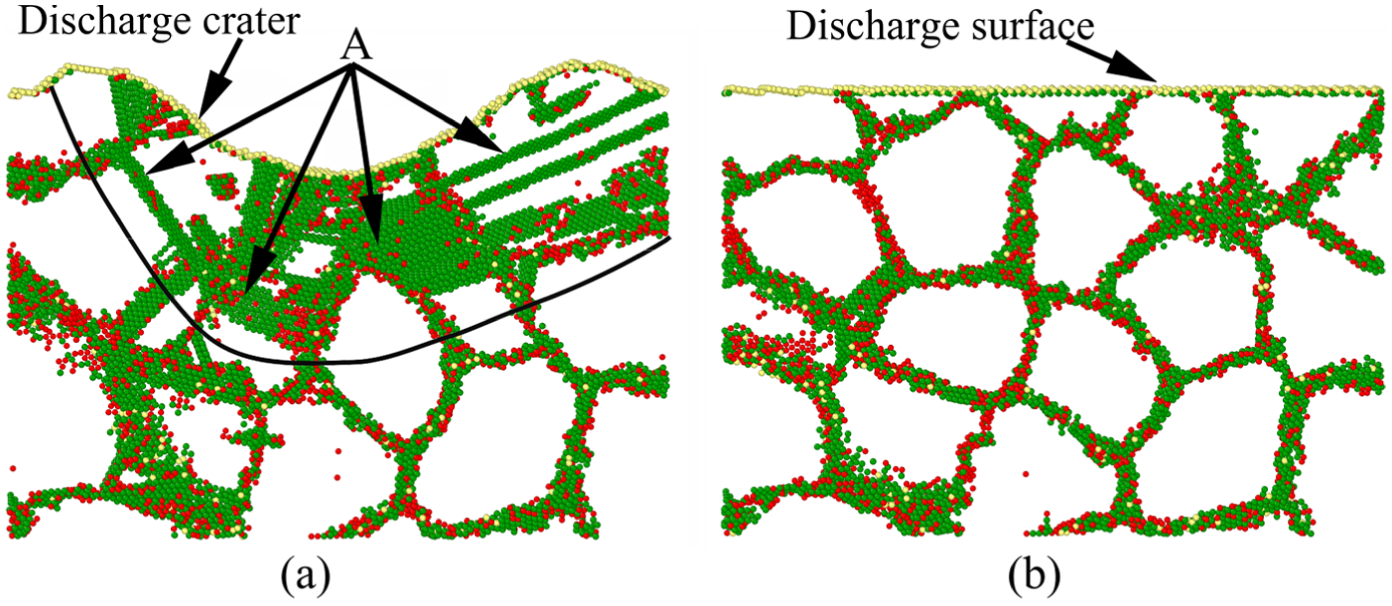
Middle sectional view of crystal defects in polycrystalline copper (a) after discharge and (b) before discharge. Atoms with perfect FCC structures were hidden to clearly show defect structures. Green atoms and red atoms stood for stacking faults (SFs) and dislocations, respectively.
Although from the middle sectional view of the electrode material in Figure 5, the crystal defects and their distributions inside the electrode are clearly shown, but this two-dimensional (2D) middle sectional view fails to exhibit more details of the defects. Thus, we used a series of horizontal sectional views to show the crystal defects distribution along the depth of the electrode, which showed much more three-dimensional (3D) details when combined with the 2D middle sectional view. The specific positions of the horizontal sectional views were shown by the black lines and corresponding capital letters in Figure 6.
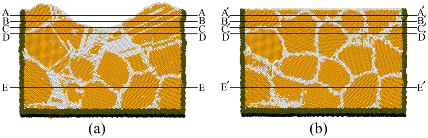
Middle sectional view of polycrystalline copper (a) after discharge and (b) before discharge. A-A, B-B, C-C, D-D, and E-E stood for positions of horizontal sectional view of electrode after discharge. A′-A′, B′-B′, C′-C′, D′-D′, and E′-E′ represented positions of horizontal sectional view of electrode before discharge.
Figure 7(a) and (b) shows the horizontal sectional views of the crystal defects after discharge and before discharge, respectively, in which the perfect FCC atoms were hidden to clearly show the defects. In this figure, A′-A′ is the horizontal sectional view of the crystal defects near the discharge surface before discharge. After discharge, the horizontal sectional view of the crystal defects in the same position is shown in A-A. From the A-A sectional view, it was found that the crystal defects were mainly bedded SFs, as shown with W. Additionally, the arrangement of atoms far away from the discharge crater was also affected by the discharge, as shown with V. B′-B′ and B-B are the horizontal sectional views of the crystal defects below A′-A′ and A-A before and after discharge, respectively. From B-B, it was found that the defects were much more than those in A-A, and the bedded SFs remained dominant. Then, below the B′-B′ and B-B views are C′-C′ and C-C before and after discharge, respectively. Compared with A-A and B-B, the defects increased continuously and their range also increased. Then, in the D-D, the defect density was much higher, and the defects mainly concentrated just below the discharge crater. At a distance from the discharge crater is the E-E view, where the material in this position was hardly affected by discharge because the arrangement of atoms in E-E and E′-E′ were almost the same. Thus, from the above analysis, the results demonstrate that after discharge, numerous defects were generated under and around the discharge crater and bulge, and the bedded SFs took a dominant role.
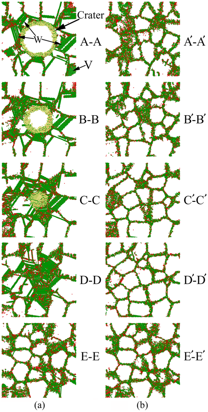
Horizontal sectional views of crystal defects in polycrystalline copper (a) after discharge and (b) before discharge. Perfect FCC atoms are hidden to clearly show defect structures. Green and red atoms stood for stacking faults (SFs) and dislocations, respectively. A-A, B-B, C-C, D-D, E-E,A′-A′, B′-B′, C′-C′, D′-D′, and E′-E′ correspond to those in Figure 6.
From the above analysis, during the discharge process, large amounts of defects were generated inside the electrode material. Then, the number change in crystal defects in polycrystalline and monocrystalline copper after discharge is shown in Figure 8. A logarithmic coordinate was adopted. From Figure 8, the results indicate that both dislocation and SFs in polycrystalline and monocrystalline copper increased greatly after discharge. However, the increasing amplitude of defects in polycrystalline copper was larger than that in monocrystalline copper. Specifically, the increasing number of SFs in polycrystalline copper was almost 15 times more than that in monocrystalline copper. Thus, during the EDM process, compared with the polycrystalline material, the monocrystalline material more easily obtained a much higher surface quality.
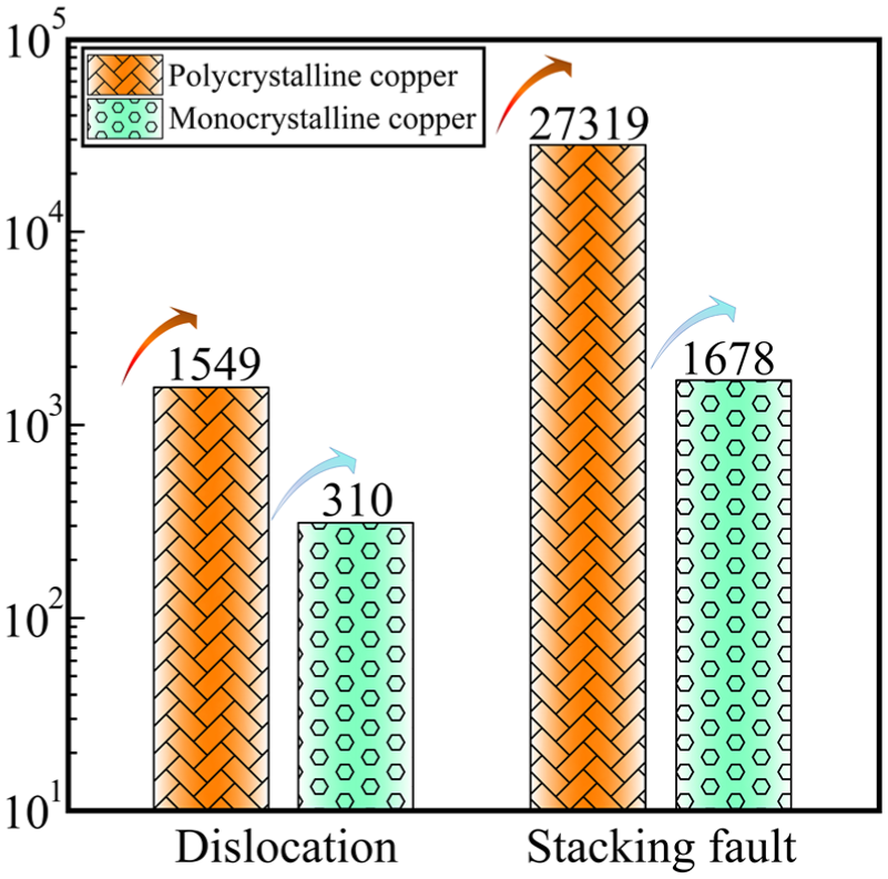
Number change in crystal defects in polycrystalline and monocrystalline copper after discharge. A logarithmic coordinate is adopted that stands for increasing number of crystal defects after discharge.
Influence of different crystal structures on morphology of discharge crater
To study the influence of different crystal structures on the discharge craters, the 3D morphology of the discharge craters in monocrystalline and polycrystalline copper is shown in Figure 9, in which the diameter and depth of the discharge crater are defined. Figure 10 shows the dimensions of the discharge craters in polycrystalline and monocrystalline copper after discharge. From this figure, the diameter of the discharge crater in polycrystalline copper was larger than that in monocrystalline copper, whereas their depths were almost the same. Figure 11 shows the volume comparison of the removal debris (the removal debris is the material totally ablated from the electrode), bulges and craters in polycrystalline and monocrystalline copper after discharge. The definitions of the removal debris, bulge, and crater were also shown in Figure 11. From this figure, in both monocrystalline copper and polycrystalline copper, the volume of the bulge was much larger than the volume of the removal debris, which indicates that in EDM, only a small quantity of the molten material was ablated from the crater, whereas most of the molten material from the crater was solidified on the discharge surface to form the bulge around the discharge crater. Additionally, from Figure 11, the volumes of both the bulge and removal debris in polycrystalline copper were larger than those in monocrystalline copper. Thus, the machining of polycrystalline copper is much easier than monocrystalline copper, which can be explained as follows. In polycrystalline copper, a large number of defects exist; thus, inside the polycrystalline electrode, a large amount of distortional energy caused by these defects is stored. During the discharge process, the distortional energy can promote the removal of the molten material. Therefore, the machining of polycrystalline copper is easier than monocrystalline copper.
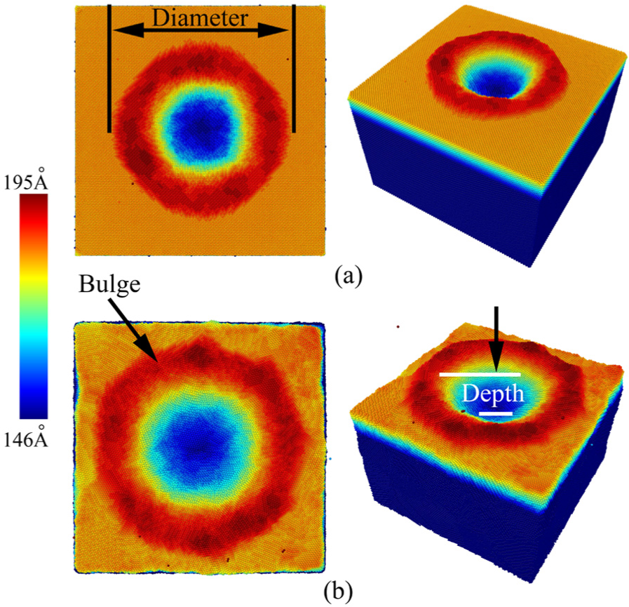
Morphology of discharge craters in (a) monocrystalline and (b) polycrystalline copper after discharge.
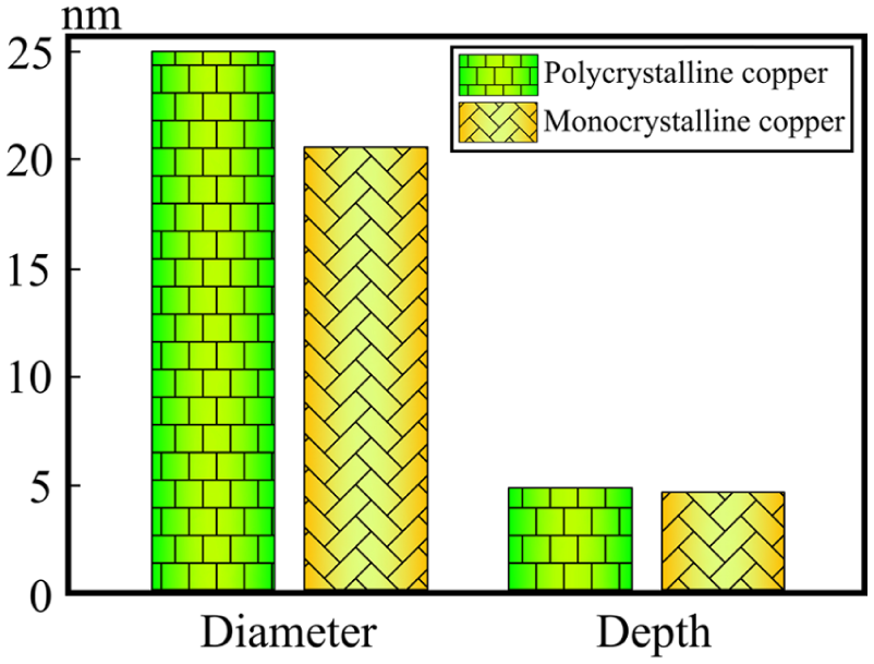
Dimensions of discharge craters in polycrystalline and monocrystalline copper after discharge.
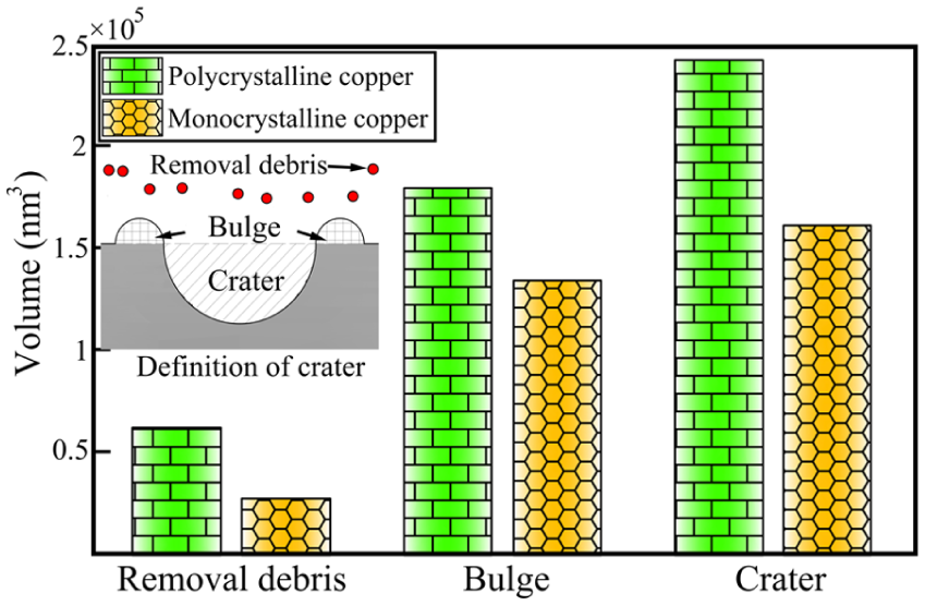
Volume comparison of removal debris, bulges, and craters in polycrystalline and monocrystalline copper after discharge.
Conclusion
In this article, the discharge in both polycrystalline and monocrystalline copper was simulated to study the material dynamics behavior. Then, the material removal processes, crystal structure evolution, and machining properties were analyzed. The following conclusions were obtained:
Compared with the discharge in the monocrystalline copper, discharge in the polycrystalline copper under the same discharge conditions caused significantly more crystal defects and much larger HAZs.
After the discharge, large amounts of SFs and dislocations were generated in the polycrystalline copper, which were mainly concentrated under the discharge crater and bulge. In those defects, the bedded SFs played a dominant role. Moreover, the farther away the defects were from the discharge crater, the sparser their distribution.
Under the same discharge conditions, the diameter of the discharge crater in polycrystalline copper was larger than that in monocrystalline copper, whereas their depths were almost the same. The volumes of both the bulge and removal debris in polycrystalline copper were larger than those in monocrystalline copper.
Due to the limitation in computer capacity, the presented model in spatial scale still cannot simulate the real EDM process. Thus, this research is a qualitative simulation of the formation and evolution process of defects, HAZs, and resolidified layers in EDM. Although the spatiotemporal scale of the model used in this simulation is significantly small compared with the real EDM, the MD simulation indeed provides an effective method to study and understand this complex process as well as provides the qualitative theoretical analysis and direction.
Footnotes
Appendix 1
Declaration of conflicting interests
The author(s) declared no potential conflicts of interest with respect to the research, authorship, and/or publication of this article.
Funding
The author(s) disclosed receipt of the following financial support for the research, authorship, and/or publication of this article: The authors would like to thank the National Natural Science Foundation of China (General Program, No. 51575136), the Key Project of Natural Science Foundation of Heilongjiang Province (No. ZD2015009) and the Key Laboratory of Micro-systems and Micro-structures Manufacturing of Ministry of Education, Harbin Institute of Technology (No. 2017KM002) for providing financial support for this research and Sandia National Laboratories (USA) for their free and open source software (LAMMPS).