
Abstract
This article describes the mechanical planarization machining of SiC substrates involving the Si face (0001) and C face (
Keywords
Introduction
Compared with conventional Si and GaAs substrates, single-crystal silicon carbide (4H-SiC) is considered one of the most promising next-generation materials for semiconductor power devices due to its excellent properties, such as its wide bandgap, high breakdown electric field, and saturated drifted velocity.1–4 6H-SiC is also an attractive substrate for group III–V nitride-based optoelectronic devices, such as blue light emitting diodes and laser diodes, due to its efficient crystal lattice matching with epitaxial GaN and its low coefficient of thermal expansion.5,6 The growth of epitaxial graphene has been reported on both the Si face (0001) and C face (
The operating performance of the Si face of SiC substrates differs from that of the C face due to the crystalline anisotropy. The majority of previous studies have investigated the polishing of the Si face.3,5,16–18 Studies on the polishing of the C face are limited. 19 Yagi et al. 20 reported that the Si face is more difficult to remove than the C face in H2O2 solutions. However, Chen et al. 21 considered that the material removal rate (MRR) of the Si face is higher than that of the C face in both mechanical polishing and chemical mechanical polishing (CMP). Due to the disparity between the MRRs of the Si face and C face, the material removal mechanisms of SiC substrates involving the Si face and C face should be further explored.
CMP, which is extensively used for the global planarization of SiC substrates, is a key technology for achieving high-quality surfaces by reducing the surface’s roughness and removing damaged layers.22–25 Although the ideal surface of SiC substrates can be achieved after CMP, removing scratches and dislocations introduced during the mechanical polishing of SiC substrates is time-consuming. In addition, the effluent liquor will contaminate the environment considerably.
Based on the principle of sol–gel (SG), a semi-fixed abrasive polishing tool with a diamond abrasive known as an SG polishing pad has been reported as an ideal polishing tool to satisfy the processing demands of scratch-free and nanoscale roughness in substrate surfaces.26–28 This planarization technique is environmentally friendly, as the deionized water is applied as a coolant without any corrosive liquid during the mechanical planarization machining. This study focused on the mechanical planarization machining of SiC substrates involving the Si face (0001) and C face (
Experimental details
Single-crystal 4H- and 6H-SiC (N-type, doping nitrogen) and 6H-SiC (V-type, doping vanadium) substrates, including the C face and Si face, were used for a comparative experiment. These substrates were purchased from Tankeblue Semiconductor Co. Ltd (Beijing, China). The SiC substrates had original surface roughnesses varying from 80 to 90 nm, a diameter of 50.8 mm, and a thickness of 400 μm. Figure 1 shows the surface morphologies of the SiC substrates, including the Si face and C face, before polishing. Polishing experiments of the SiC substrates were performed on a rotary-type polishing machine (UNIPOL-1200S, Kejing, China) with an SG polishing pad. A schematic diagram of the polishing process is presented in Figure 2. The SiC substrates were adhered to the substrate carrier by paraffin. The polishing tool was pasted on the platen using a magnetic adsorption pad. A diamond abrasive with a size of 40 μm was chosen for the polishing pad. In the process, the polishing load, rotational velocity of the workpiece, rotational velocity of the polishing pad, and processing time were 5 kg, 60 r/min, 120 r/min, and 1 h, respectively, and distilled water was used as the coolant. After processing, all substrates were cleaned immediately with ethanol and deionized water under sonication and then dried under high-pressure air.
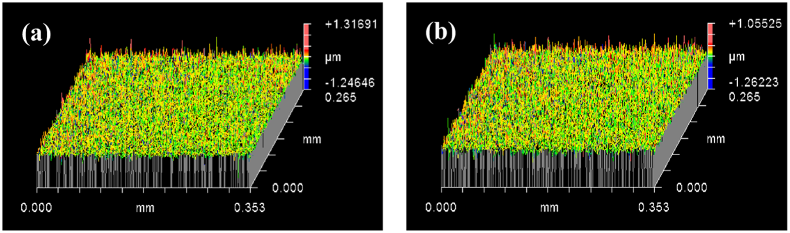
Surface morphologies of the SiC substrates, including the (a) Si face and (b) C face, before polishing.
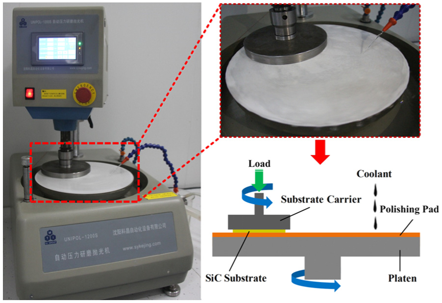
Schematic diagram of the polishing process.
The surface topographies of the substrates were measured using a three-dimensional (3D) optical surface profiler with a scanning area of 70 µm × 50 µm (Newview 7300, ZYGO, USA), and the surface roughness (Ra) was the average value of 10 areas that were evenly dispersed on the substrate surface. The weights of the SiC substrates before and after polishing were measured by a precision electronic balance with a precision of 0.1 mg (BSA224S, Sartorius, Germany) to calculate the MRRs according to the following equation29,30

where
To investigate the material removal mechanism of the SiC substrate, transmission electron microscopy (TEM), energy dispersive spectrometry (EDS), and selected area electron diffraction (SEAD) characterizations of the wear debris were performed using a Tecnai F30 field-emission gun TEM with an accelerating voltage of 300 kV. The wear debris extracted from the polishing coolant was placed 2 weeks before TEM testing to remove the gels from the coolant. A cross-sectional TEM specimen was prepared using focused ion beam (FIB) FEI Helios NanoLab 600i installation. The microstructure of the TEM specimen was investigated by high-resolution TEM.
The normal force of the single active grain in the SG polishing pad should be calculated and the nanomechanical properties of the SiC substrate should be tested to further verify the removal mechanism of SiC substrates. The surface topography of the SG polishing pad and the number of active grains can be measured by a white light optical interferometer (WYKO NT 9300, Bruker, USA). A nanomechanical test instrument (Triboindenter®; Hysitron Inc., USA) was employed on the SiC specimens for nanoindentation and nanoscratching at room temperature. The SiC specimens were epi-ready with a surface roughness (Ra) of less than 0.2 nm. The standard Berkovich indenter was used for nanoindentation, and a conical diamond probe with a tip radius of 3 μm was used for nanoscratching. The normal load during scratching was held constant at 4 mN. The scratching velocity was set at 1.0 μm/s.
Results and discussion
Surface characteristic and MRR of the SiC substrates
The surface topographies of the SiC substrates after polishing are shown in Figure 3. A scratch-free and smooth substrate surface can be achieved after processing by the SG polishing pad, and only a few pits exist on the SiC substrate surface. The polished C face is smoother than the polished Si face because only several superficial pits remain on the C face, whereas several deep and large pits exist on the Si face. As shown in Figure 4(a), the surface roughness of the C face (<2 nm) is lower than that of the Si face. This trend also occurs in N-type 4H-SiC, N-type 6H-SiC, and V-type 6H-SiC. Moreover, the MRRs of the C faces are higher than those of Si faces, as shown in Figure 4(b). For instance, the MRR of the C face is 45.9%, 127.4%, and 61.7% larger than that of the Si face for N-type 4H-SiC, N-type 6H-SiC, and V-type 6H-SiC, respectively. Thus, the C face is more easily removed than the Si face during mechanical planarization machining.
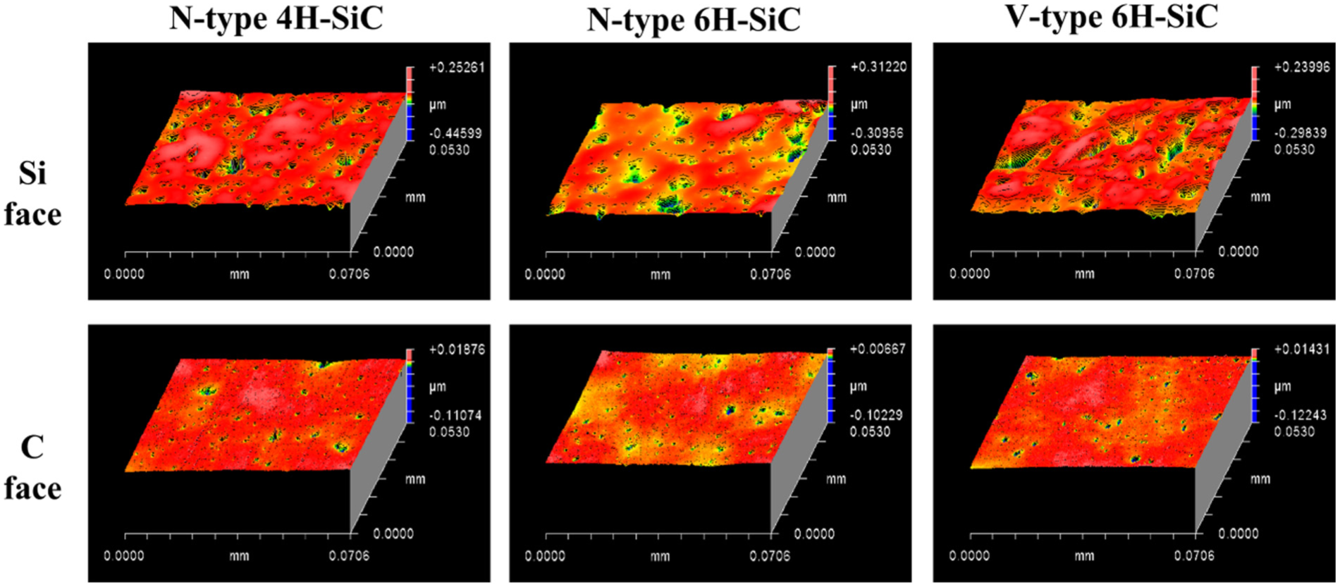
Surface topographies of the SiC substrates after polishing.
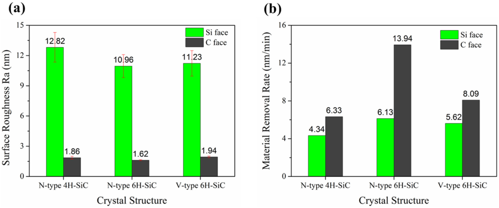
Surface roughness (a) (Ra) and (b) MRR of the SiC substrates.
As illustrated in Figure 4(b), the MRRs of N-type 6H-SiC containing the Si face and C face are higher than those of N-type 4H-SiC. 4H-SiC is a hexagonal lattice structure with an ABCB stacking sequence, similar to 6H-SiC, which has an ABCACB stacking sequence. 31 Thus, the difference between the MRRs of N-type 4H-SiC and N-type 6H-SiC is likely determined by their stacking structure period. In addition, for 6H-SiC, the MRR of the N-type SiC substrate is larger than that of the V-type SiC substrate. Certain dopants, such as doping nitrogen (N-type) and doping vanadium (V-type), have been added to the crystal during the growth process to obtain the unique substrate properties. However, the integrity of the crystal structure will be affected by the dopants. The degree of the effect of the dopants on the crystal structure depends on the doping concentration. The doping concentration of the N-type SiC substrate is 1.0 × 1018 cm−3 higher than that of the V-type SiC substrate (8.0 × 1016 cm−3), making the influence degree of N-type SiC substrate larger than that of the V-type SiC substrate. Once the integrity of the crystal structure is contaminated, the mechanical properties of the material will be decreased and can be easily removed. Thus, the variation in the MRRs of N-type 6H-SiC and V-type 6H-SiC is attributed to the doping concentration of the crystal. In summary, the crystalline structure and doping concentration of the crystal significantly affect the MRR of the SiC substrate.
Characterization of the material removal mechanism
To investigate the material removal mechanism of the SiC substrate, the 6H-SiC wear debris on the Si face and C face produced during the process was observed. The TEM images, SAED patterns, and EDS spectra of the wear debris extracted from the coolant are presented in Figure 5. The SAED patterns and EDS spectra correspond to the relevant area of the TEM images. The Cu in the EDS spectrum originated from the micrograte, and the segmental C was also derived from the micrograte. Accordingly, Figure 5(a) shows the wear debris of the Si face, and Figure 5(d) shows the wear debris of the C face. The wear debris of the Si face is fragmented with a size of approximately dozens of nanometers, and the wear debris of the C face is granular with a size of several hundred nanometers. As shown in Figure 5(b) and (e), the halo in the SAED patterns suggests that the SiC wear debris on the Si face and C face is in the amorphous phase. The TEM results indicate that the wear debris size of the C face is larger than that of the Si face, and the crystalline states of both faces are amorphous.
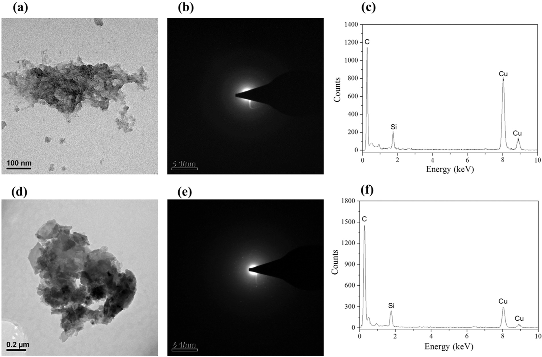
(a, d) TEM images, (b, e) SAED patterns, and (c, f) EDS spectra of the wear debris: (a–c) the wear debris of the Si face and (d–f) the wear debris of the C face.
Figure 6 shows the cross-sectional TEM image of the polished 6H-SiC substrate (Si face). Only a thin amorphous layer (approximately 2 nm) is detected on the cross section of the SiC substrate, and no other subsurface damage, such as dislocation and cracking, is observed. Thus, an ultrathin amorphous damage layer emerges on the surface of the monocrystalline SiC substrate after processing by the SG polishing pad. The result of the phase transformation for the SiC substrate from the crystalline state to the amorphous state during polishing is consistent with the wear debris results.
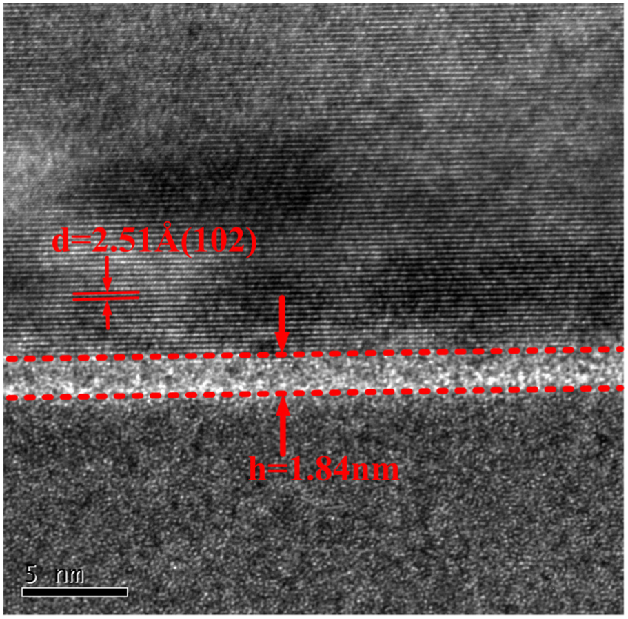
Cross-sectional TEM images of the polished 6H-SiC substrate (Si face).
The TEM results indicate that the wear debris size of the C face is larger than that of the Si face. The average size of the wear debris can be defined as the material removal scale. 32 Therefore, the material removal scale of the C face is larger than that of the Si face. This condition indicates that the variation in the MRRs is determined by the material removal scale under the same conditions. The TEM results also demonstrate that the SiC substrates are removed through amorphization, and only an ultrathin amorphous damage layer exists on the SiC substrate. The processing of substrates through the SG polishing pad is dominated by the mechanical removal of the SiC material, as no apparent evidence of a chemical reaction was observed in the TEM investigation.
Mechanical characteristics of SiC substrates
The mechanical characteristics of SiC substrates should be investigated to further verify the material removal mechanism. The normal force of a single active grain in the SG polishing pad should be defined before testing the mechanical characteristics of the SiC substrates. Figure 7(a) shows the surface morphology of the SG polishing pad before processing. The diamond abrasives are homogeneously dispersed in the matrix, and no evident aggregation can be observed in the SG polishing pad. In our previous work, 28 we found that the diamond abrasives will yield to the matrix and then stay on a contour line. The protrusion heights of abrasives were fixed at approximately 11 μm after polishing. Diamond abrasives with a protrusion height of more than 11 μm can be defined as active grains. The active grains corresponding to Figure 7(a) are presented in Figure 7(b), and there are 17 active grains in an area of 0.8 mm × 0.8 mm. The average number of active grains is approximately 14.1, as calculated from 10 different areas (0.8 mm × 0.8 mm). Therefore, the normal force of a single active grain can be calculated by the following equation
where m (kg) is the polishing load, g (m/s2) is the acceleration of gravity, µ is the contact factor, A is the contact area, S is the single measuring area, Q is the average number of active grains in the SG polishing pad, and F is the normal force of a single active grain. m, g, µ, A, S, and Q are equal to 5 kg, 10 m/s2, 0.3, 20.27 cm2, 0.64 mm2, and 14.1, respectively. The normal force of a single active grain F is calculated to be 3.73 mN.
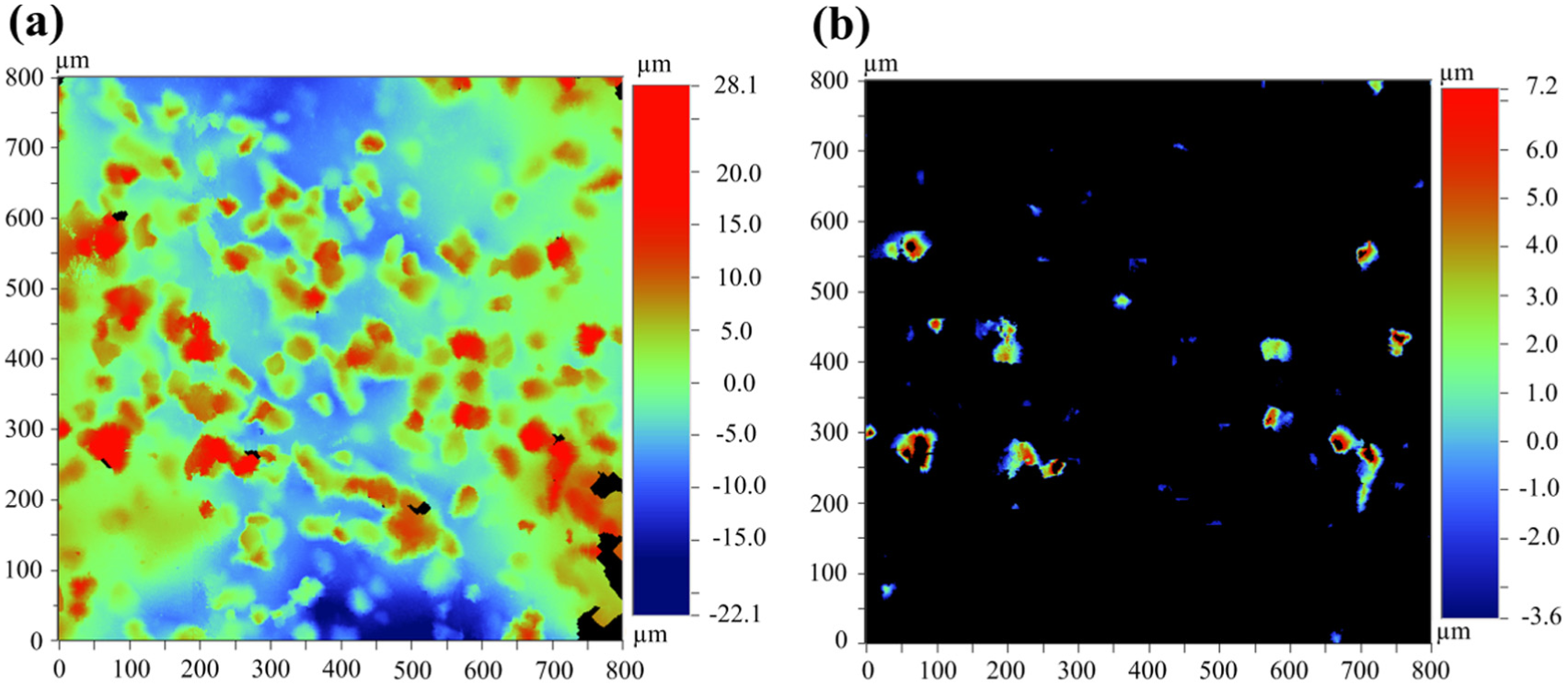
Surface morphology of the (a) SG polishing pad and (b) active grains.
Nanoindentation was performed on the SiC specimens to test the deformation characteristics of the substrate subsurface. Figure 8 shows the representative load–displacement (P–h) curves of the 6H-SiC substrate, including the Si face and C face, during nanoindentation. Multiple displacement discontinuities or pop-in events occur during loading. The load corresponding to the first pop-in event can be defined as the critical indentation load (Pc). 33 The critical indentation loads (Pc) of the Si face and C face are approximately 2.3 and 1.5 mN, respectively. The deformation is purely elastic before the pop-in event and elasto-plastic after the pop-in event. The calculation results demonstrate that for the normal force of a single active grain, the removal mechanism of SiC substrates processed by the SG polishing pad is elasto-plastic. The effective indentation modulus (Er) of the indentation system can be directly obtained from the nanoindentation instrument based on the Oliver–Pharr method. 34 The average Er of the Si face (387.51 GPa) is larger than that of the C face (266.02 GPa), indicating that the Si face is more difficult to remove than the C face.
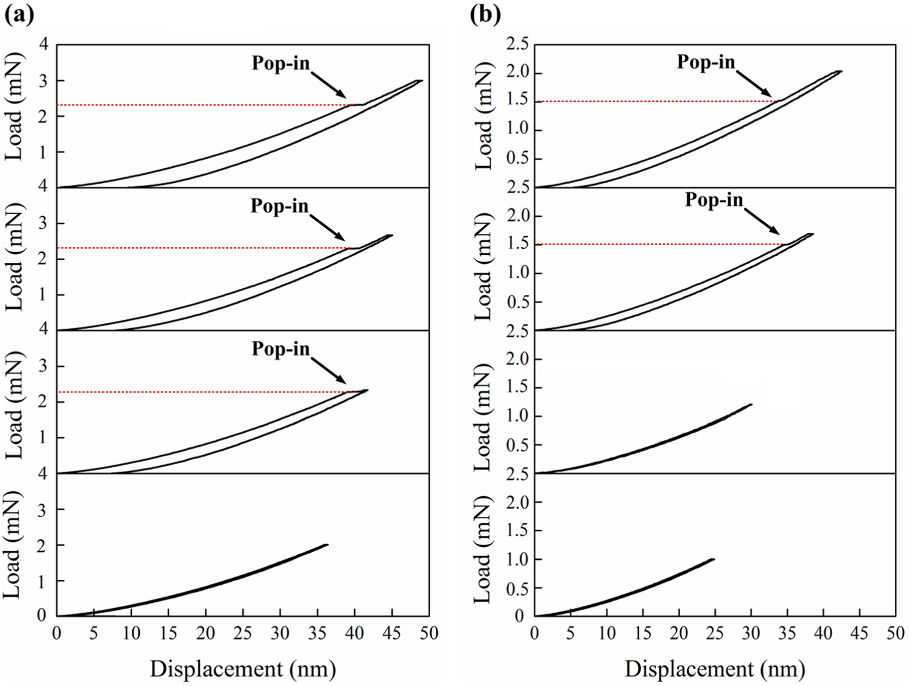
Load–displacement (P–h) curves of the 6H-SiC substrate: (a) Si face and (b) C face.
Nanoscratching tests were performed on the same SiC specimens. Figure 9 shows the friction coefficient obtained by scratching the surfaces under a constant normal load of 4 mN. The friction coefficient of the Si face is smaller than that of the C face. The average friction coefficients of the Si face and C face are 0.1778 and 0.2176, respectively. A larger friction coefficient is associated with a higher removal rate under the same conditions. Thus, the C face is easier to remove than the Si face.
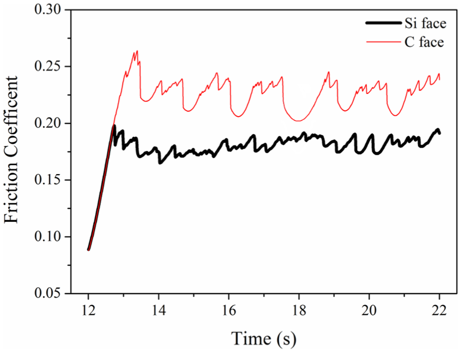
Friction coefficient obtained from scratching the surfaces under a constant normal load of 4 mN.
The critical indentation loads (Pc) of the Si face and C face are less than the normal force of a single active grain in the SG polishing pad, thereby demonstrating that the removal mode of SiC substrates processed by the SG polishing pad is elasto-plastic. The average Er of the Si face is larger than that of the C face, and the average friction coefficient of the Si face is lower than that of the C face, indicating that the Si face is more difficult to remove than the C face. This result is consistent with the MRR results. Therefore, the SiC mechanical characteristics can further verify the material removal mechanism of the SiC substrate. In addition, amorphization, including the wear debris and subsurface damaged layer shown in TEM results, is induced by a mechanical load rather than by a chemical factor.
These results demonstrate that the differences between the MRRs of the Si face and C face depend on the material removal scale and the mechanical characteristics of the substrates. The C face is easier to remove than the Si face in mechanical planarization machining. In addition, the crystalline structure and doping concentration of the crystal significantly affect the MRR of the SiC substrate. The achieved smoothness and scratch-free substrate surface with nanoscale roughness before CMP is a suitable pre-machined surface, which shortens the total processing time and reduces the cost. Understanding the removal mechanisms of SiC substrates is critical for the finishing process.
Conclusion
This work investigated the mechanical planarization machining of 4H- and 6H-SiC substrates, including the Si face and C face, using an SG polishing pad. Scratch-free SiC substrate surfaces with nanoscale roughness can be achieved after processing by the SG polishing pad. The C face is easier to remove than the Si face due to its higher MRR in the mechanical planarization machining. The crystalline structure is the major factor affecting the MRR of 4H- and 6H-SiC substrates. The doping concentration of the crystal significantly affects the MRR of the N-type and V-type SiC substrates. The variation of the MRRs between the Si face and C face is determined by the material removal scale. The mechanical characteristics of the SiC substrates also confirm that the C face is easier to remove than the Si face during mechanical planarization machining. The processing of substrates using an SG polishing pad is dominated by the mechanical removal of the SiC material.
Footnotes
Acknowledgements
The nanoindentation and nanoscratching experiments were performed at the School of Engineering, University of Queensland, Australia. The authors express their gratitude to Prof. Han Huang et al. for their support.
Declaration of conflicting interests
The author(s) declared no potential conflicts of interest with respect to the research, authorship, and/or publication of this article.
Funding
The author(s) disclosed receipt of the following financial support for the research, authorship, and/or publication of this article: This research is supported by the National Natural Science Foundation of China (Grant No. 51475175) and the Specialized Research Fund for the Doctoral Program of Higher Education (Grant No. 20133501130001).