
Abstract
In recent times, nickel-based super alloys are widely utilized in aviation, processing, and marine industries owing to their supreme ability to retain the mechanical properties at elevated temperature in combination with remarkable resistance to corrosion. Some of the properties of these alloys such as low thermal conductivity, strain hardening tendency, chemical affinity, and presence of hard and abrasives phases in the microstructure render these materials very difficult-to-cut using conventional machining processes. In this work, an experimental setup was developed and integrated with the existing electrical discharge machining system for carrying out powder-mixed electrical discharge machining process for Inconel 625. The experiments were planned and conducted by varying five different variables, that is, powder concentration, peak current, pulse-on time, duty cycle, and gap voltage based on the central composite design of response surface methodology. Effects of these parameters along with powder concentration were investigated on various surface integrity aspects including surface morphology, surface roughness, surface microhardness, change in the composition of the machined surface, and residual stress. Results clearly indicated that addition of powder to dielectric has significantly improved surface integrity compared to pure dielectric. Among the powders used, silicon has resulted in highest microhardness, that is, almost 14% more than graphite. Lowest surface roughness (approximately 50% less than pure kerosene) and least residual stress were obtained using silicon powder (approximately 8% less than graphite-mixed dielectric). Relative content of nickel was reduced at the expense of Nb and Mo after addition of powders like aluminum and graphite in dielectric during electrical discharge machining.
Keywords
Introduction
The rare synergy of high yield strength, corrosion resistance, and the ability to withstand high temperatures allows the usage of nickel-based super alloys in the industries like aerospace, marine, power plant, and chemical processing. 1 Conventional machining of these alloys becomes extremely difficult due to their high-temperature resistance resulting in the formation of built-up edge at tool tip. Such difficult-to-machine materials would be better machined through non-traditional machining processes. Electrical discharge machining (EDM) is one of the most frequently used non-traditional machining processes to cut any electrically conductive material without regard to its physical and mechanical characteristics. In EDM, localized melting and explosion of workpiece occurs due to the spark energy generated in the electrode gap between tool and electrode. Peak current, pulse time, gap voltage, and duty cycle are some of the most influencing process variables that affect the EDM characteristics of nickel-based super alloys.2–8 Though all electrically conductive materials (including nickel-based super alloys) are successfully machined in EDM, low productivity and poor surface quality of the machined surface restrict its large-scale application in industries. The addition of some suitable conductive powders in dielectric during EDM resulted in higher productivity without much sacrifice on the surface quality. The method is known as powder-mixed electrical discharge machining (PMEDM). The impregnated powders enhance the overall electrical conductivity of the dielectric and allow the discharge to occur from a bigger range. The increased discharging frequency and improved flushing conditions, as well as multiple sparks, ensure improvement in both material removal rate (MRR) and surface quality.
Al powder-dispersed dielectric, yielded larger MRR in comparison with Si powder during the EDM of Inconel 718. This is due to high energy transfer to workpiece owing to high electrical and thermal conductivities of Al. 9 MRR increased with peak current, pulse-on time, gap voltage, and duty cycle due to the rise in spark energy during the EDM of hastelloy using Al particles mixed dielectric. 10 MRR improved with powder concentration due to the augmentation of multiple sparks and sparking frequency. But for too large quantities of powder, MRR started declining due to sticking and agglomeration of Al particles in electrode gap. 11 Surface roughness (SR) declined and later climbed with powder concentration. Initial decrease was due to the discharge column expansion and the increase was due to sticking and agglomeration effects. The combination of cryogenically treated copper electrode and graphite powder-suspended dielectric decreased the electrode wear ratio (EWR) during the EDM of Inconel 718. 12 Refined grains of electrode material prevented the tool wear. Micro-drilling of Inconel 718 using molybdenum disulfide-dispersed dielectric, improved the MRR compared to conventional micro-drilling using EDM. 13 Considerable improvement in both MRR and surface finish was achieved during the EDM of Inconel 825 by impregnating single as well as multi-walled carbon nanotubes (CNTs) in dielectric. Low-density, high electrical and thermal conductivities of CNTs allowed uniform distribution of discharge heat.14,15
From the study of past research work, it is observed that PMEDM has strong potential in enhancing MRR and surface finish of nickel-based super alloys. However, the procedure for powder material selection, based on specific requirements and application, is still unknown. Therefore, it is essential to comparatively evaluate the performance of some of the commercially available powders and correlate the same with different properties of these powder materials. While MRR and surface finish undoubtedly have enormous significance, surface integrity of the machined components perhaps plays a more vital role in influencing the performance during their intended applications and deciding the service life of the same components. It is also observed from the literature that various methodologies were adopted to analyze different response characteristics in PMEDM. However, very few attempts have been made to correlate the interaction effect of PMEDM process parameters with process performance. Few studies pertaining to EDM and PMEDM evaluated basic machining characteristics of Inconel 718. However, different other grades of super alloy with variation in chemical composition and properties should also be considered in order to attain deeper insight into the role of process mechanics on such alloys. Inconel 625 is one such grade of nickel-based super alloys of which EDM characteristics and role of powder materials have hardly been evaluated.
Considering all the gaps or incompleteness in the reviewed literature discussed above, the major objective of this research work is to study the effect of various powder additives and process variables on various aspects of surface integrity such as machined surface morphology, SR, surface microhardness, change in chemical composition, and residual stress of Inconel 625 after PMEDM process.
Experimental procedure
All experiments were conducted on a die sinking EDM machining setup (ElektraPlusPS 50ZNC; Electronica, India) as shown in Figure 1. Since it was planned to use a fresh dielectric fluid with varying concentrations of powder for every experiment, an independent dielectric recirculation setup was designed, manufactured, and arranged with the existing machine as indicated in Figure 1.
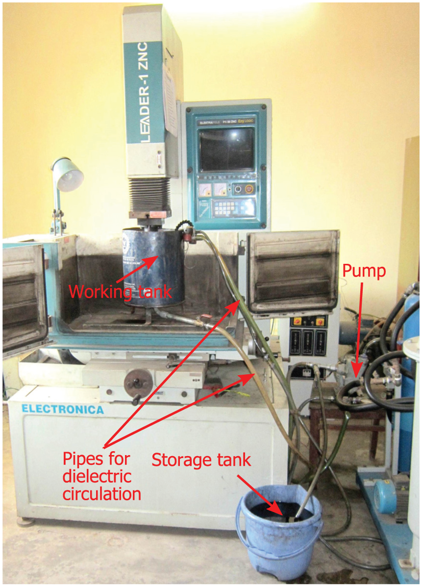
Experimental setup.
The recirculation system consists of a cylindrical working tank of 20 L, a work holding fixture, a dielectric reservoir (bucket), a 0.5 HP pump, and delivery pipes. A pressure gauge was also attached to the system to measure the dielectric pressure during experimentation. The pump receives the dielectric fluid from the outlet of the cylindrical tank and recirculates it to the tool-work inter-electrode gap to flush out the debris. The continuous circulation of the dielectric fluid avoids the settlement of powder particles in the flushing system. In the current investigation, side jet flushing was selected to flush out the debris.
Materials
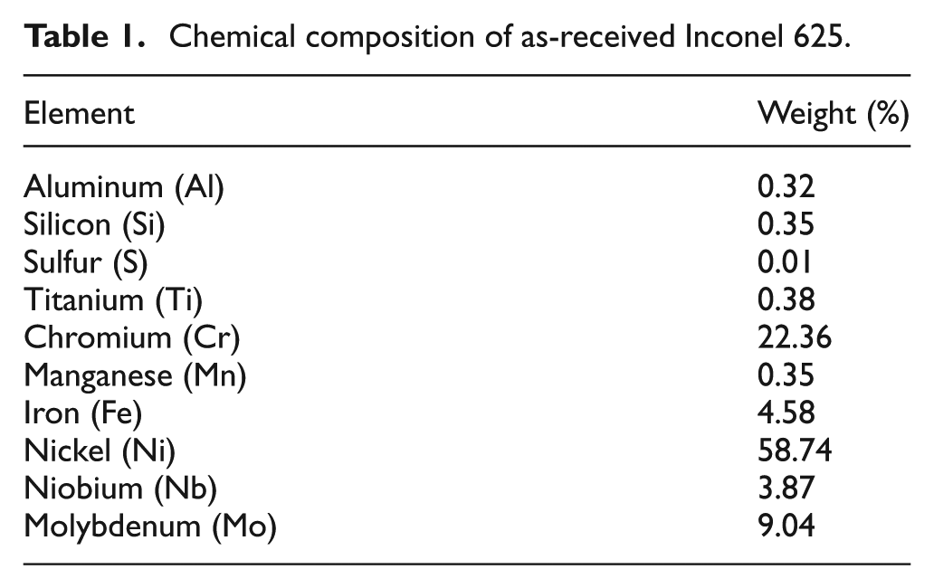
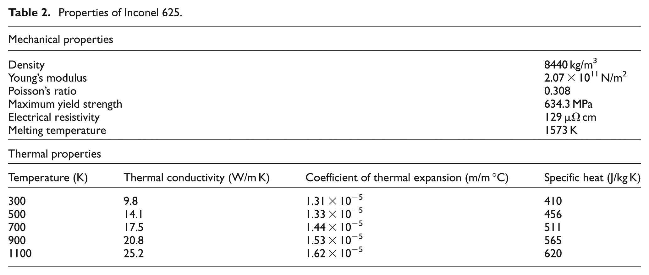
Inconel 625 was chosen as the workpiece material in the form of thin plates with dimensions of 40 mm × 40 mm × 5 mm. Chemical composition and properties of Inconel 625 are listed in Tables 1 and 2, respectively. An electrolytic copper tool of 12 mm diameter 60 mm has been used to perform the experiments.
Chemical composition of as-received Inconel 625.
Properties of Inconel 625.
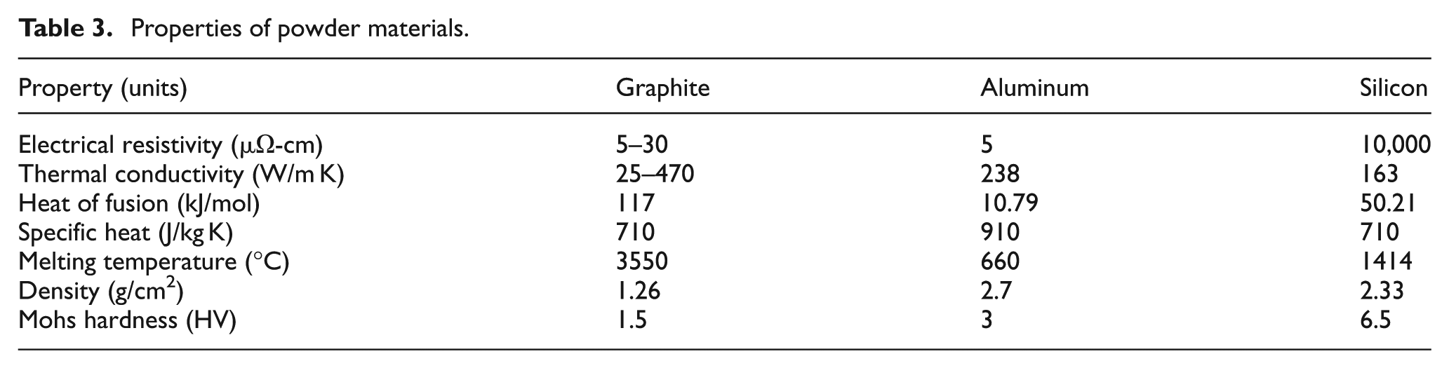
Three different powders, that is, aluminum (Al), graphite, and silicon (Si) that are significantly different with respect to their thermo-physical characteristics as shown in Table 3 were mixed in kerosene dielectric. The average particle size of all the three powders (Sigma-Aldrich) is ∼15 µm.
Properties of powder materials.
Machining conditions
Five process parameters, that is, powder concentration (Cp), peak current (Ip), pulse-on time (Ton), duty cycle (τ), and gap voltage (Vg) were selected for this research work. Choice of parameters was influenced by the fact that these parameters have significant impact on various EDM and PMEDM characteristics. Lateral flushing, having a pressure of 0.5 kg/cm2 and positive polarity (workpiece as anode), was used for all the experiments. Tool working time and lift time were set to be 0.7 s and 0.3 s, respectively. Servo sensitivity (SEN) which controls the speed of quill was chosen as 7. Anti-arc sensitivity (ASEN) which does not allow sparking when electrode gap is not clean was set to be 5. Depth of machined hole of 1 mm was kept same for all the samples throughout.
Plan of experiments
The experiments were planned according to central composite design (CCD) of response surface methodology (RSM). The process variables and their levels are provided in Table 4. The ranges of the parameters were so chosen that the process falls under semi-finishing operation. Second order polynomial can be fit using CCD. Curvature effect is also taken care of by CCD. In this research work, half factorial 2K design was chosen to minimize the experimental runs. Half factorial 32 run (25) unblocked design having 16 factorial points, 10 axial points, and 6 center points is considered for experimentation. According to the experimental design, 32 number of runs for each powder was obtained. Therefore, one complete set of experiment involves 96 number of runs. Each of the runs was repeated twice so that a total of 96 × 2 number of experimental runs were performed in the entire study.
Process parameters and their levels.
Measurement of responses
A scanning electron microscopy (SEM) (JSM-6480; JEOL, Japan) along with energy dispersive spectroscopy (EDS) through X-ray was used to reveal the morphology, cracks, and altered layers of the machined surface. Measurement of SR (center line average, Ra) was recorded using a portable stylus type profilometer (Surtronic 3+; Taylor Hobson, UK). The cut off and sampling lengths were set to be of 0.8 and 4 mm, respectively. Measurements were carried out at three randomly chosen locations on each of the machined specimens. The average of three values was taken as the SR of a particular specimen. Microhardness of the machined surfaces was determined at three random locations using a Vickers microhardness tester (LV 700; Leco, USA). During measurement, a load of 50 g was applied with a dwell time of 15 s. The mean value was determined by taking the average of three measured values. The residual stress on the machined surfaces was determined using sin2ψ technique while performing the measurement in a high-resolution XRD system (HRXRD; PANalytical, The Netherlands). First, the major phase, that is, peak with highest intensity was identified from trial measurements which revealed (1 1 1) peak observed at 2θ = 42.75° using Cu (λ = 1.5418 A°) radiation. The lattice spacing measurement was performed in 7ψ tilts. The Lorentz polarization, Kα-2 splitting, and background corrections were performed for the measured intensities. Peaks were analyzed using the Gaussian curve fit.
Results and discussion
Surface morphology
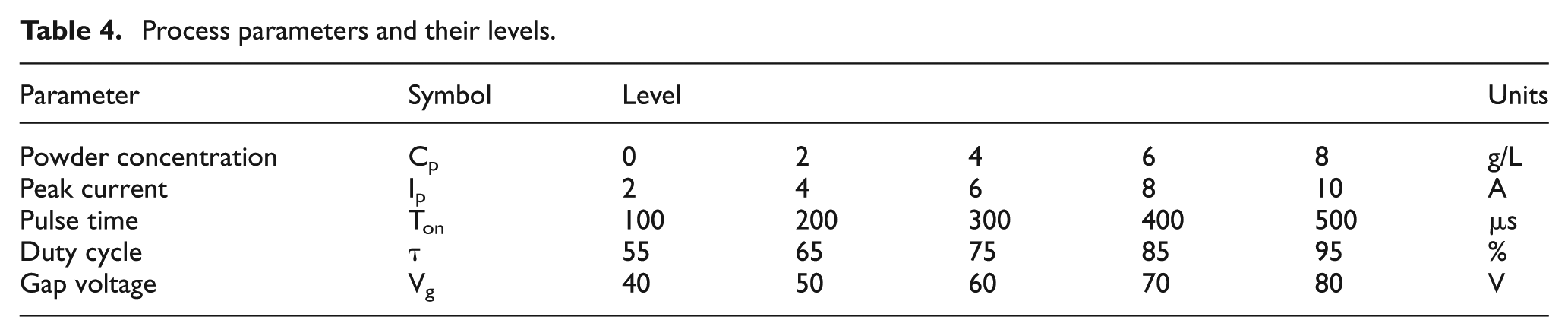
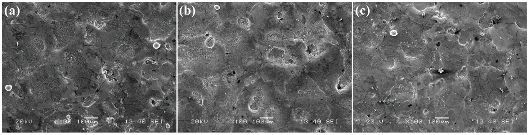
SEM images in Figure 2 show the crater topography of the cut surface using three powder-mixed dielectrics. Profound and tiny cavities were noticed on the surface cut by conventional EDM (Figure 2(a)). For all the three powder-mixed dielectrics, larger and shallower cavities were noticed compared to conventional EDM. This is due to increased electrical conductivity which generates spark from a big distance. Lengthy electrode gap permits the spread of plasma channel width. Parallely, hydrostatic force operating on the plasma channel diminishes. Consequently, big and facile craters are created on the workpiece since spark energy spreads over a bigger region. Among the used powders, graphite generated biggest craters due to the combination of its low-density, high electrical and thermal conductivities as shown in Table 3. It is followed by aluminum and silicon. However, the difference in crater size among the three powder-mixed dielectrics is very small.
Surface morphology using (a) no powder, (b) graphite, (c) aluminum, and (d) silicon powders for Cp= 4 g/L, Ip = 6 A, Ton = 300 µs, τ = 75%, and Vg = 40 V.
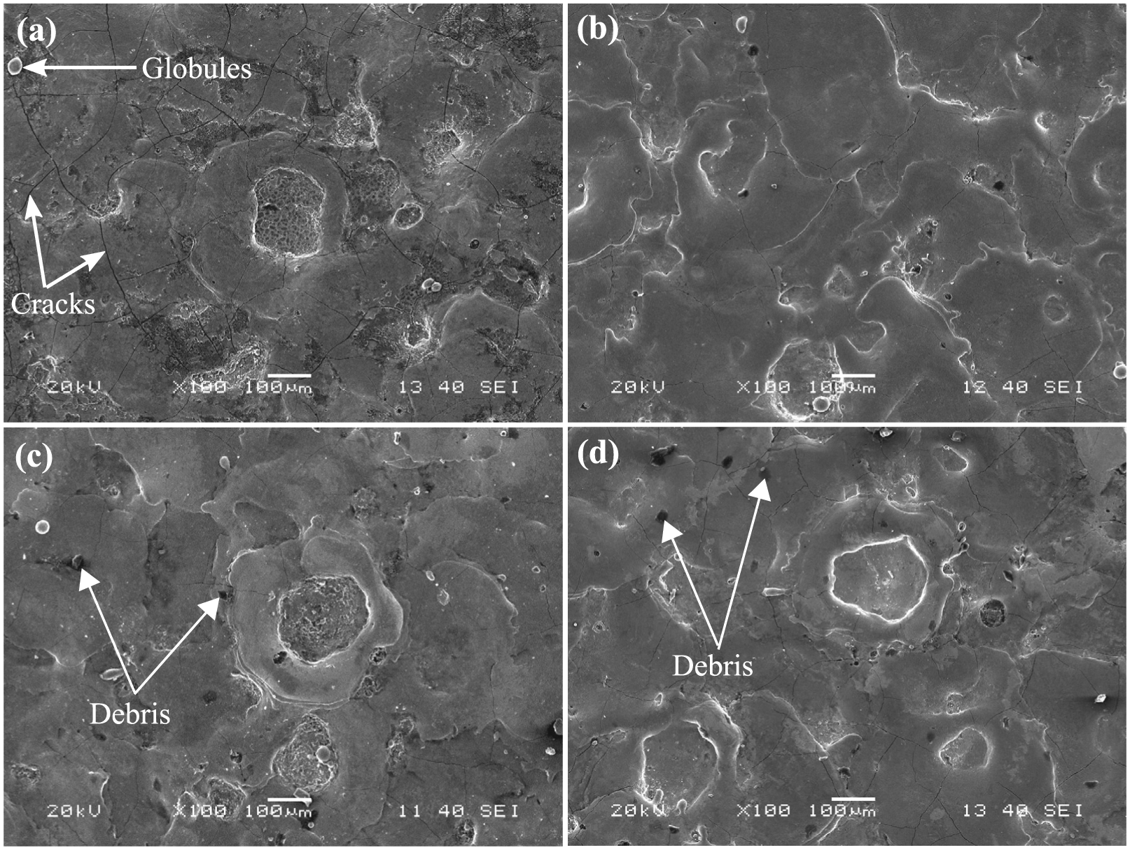
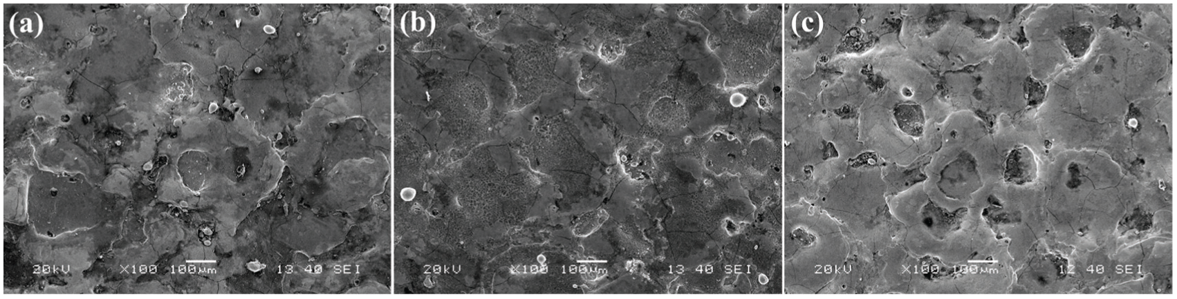
Crater size increased at high powder concentration (8 g/L) compared to low powder concentration (4 g/L) as shown in Figure 3. This is due to the increased spark gap allowing the plasma channel expansion with powder addition.
Surface morphology using (a) graphite, (b) aluminum, and (c) silicon powders for Cp = 8 g/L, Ip = 6 A, Ton = 300 µs, τ = 75%, and Vg = 40 V.
Figure 4 shows the crater distribution at a peak current of 2 A. The craters are small, flat, and distinctly visible. It is due to the small amount of discharge energy associated with low peak current.
Surface morphology using (a) graphite, (b) aluminum, and (c) silicon powders for Cp = 4 g/L, Ip = 2 A, Ton = 300 µs, τ = 75%, and Vg = 40 V.
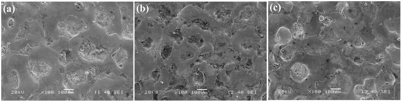
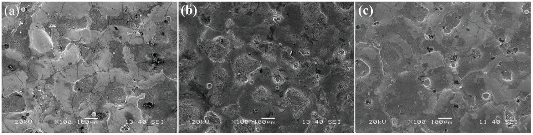
Large, flat, and distinct craters were observed at a pulse-on time of 500 µs as shown in Figure 5. Larger craters are due to the expansion of plasma channel with pulse-on time. Reduction in plasma channel pressure also allows the molten material to flow over a large area.
Surface morphology using (a) graphite, (b) aluminum, and (c) silicon powders for Cp = 4 g/L, Ip = 6 A, Ton = 500 µs, τ = 75%, and Vg = 40 V.
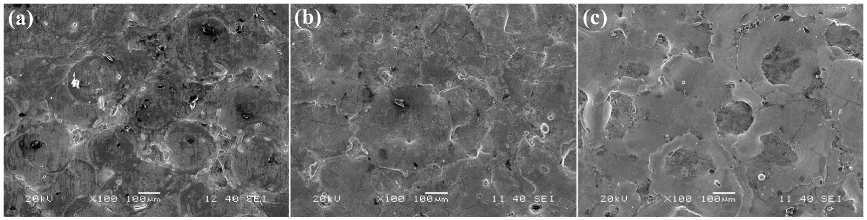
Crater size increased slightly with the increase in duty cycle as shown in Figure 6. This may be due to the flow of molten metal at the crater edges as the time available for debris removal is very short. Craters also appeared to be deep due to bulging of molten metal at the crater edges because of insufficient cooling time.
Surface morphology using (a) graphite, (b) aluminum, and (c) silicon powders for Cp = 4 g/L, Ip = 6 A, Ton = 300 µs, τ = 95%, and Vg = 40 V.
Crater diameter slightly increased with gap voltage due to enlargement of electrode gap at higher voltages. Comparatively, shallow craters were obtained as shown in Figure 7 due to the decreased plasma channel pressure on the molten metal.
Surface morphology using (a) graphite, (b) aluminum, and (c) silicon powders for Cp = 4 g/L, Ip = 6 A, Ton = 300 µs, τ = 75%, and Vg = 80 V.
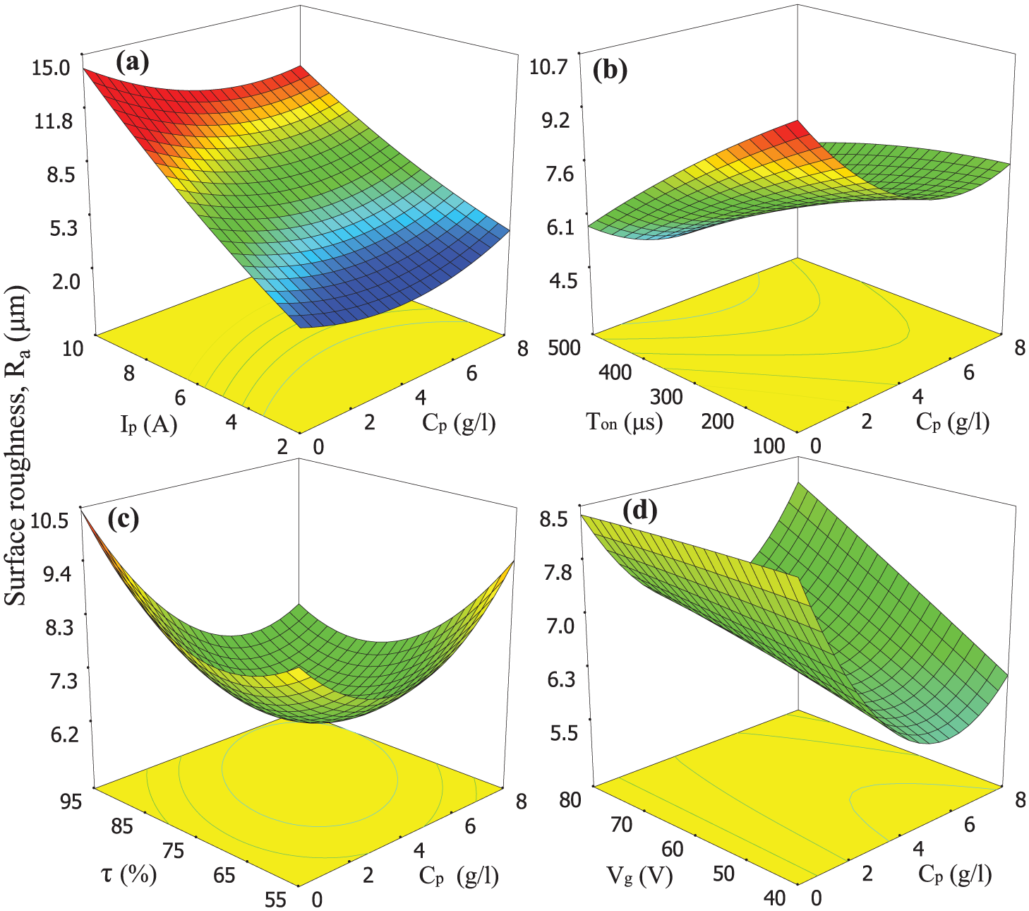
Surface roughness
A considerable reduction in SR occurred with the mixing of suitable powders such as Al, graphite, and Si with the dielectric. Plasma channel gets widened and enlarged when powders are added to the dielectric. Multiple and random discharges among powders, distribute the thermal energy over a large region. As a consequence, big and facile cavities are generated on the machined surface. 16
Besides, the melted material is lightly compressed by the plasma channel. Hence, entrapping of gas is reduced in the cavities. As a result, the surface becomes flat, uniform, and smooth. 17 Figures 8–10 show the effect of different powders and control variables on SR. Discharge energy increases with peak current causing an hike in impulsive force and removing more molten and gasified materials. This generates deep and large discharge cavities leading high-SR. However, SR slightly decreased with increase in pulse-on time. This may be due to the expansion of discharge column leading to large and shallow cavities. An increase in SR was noted with the raise in duty cycle. This is attributed to the predominant influence of spark energy per pulse leading to deeper cavity and insufficient time for flushing debris. Surface became rough with gap voltage with the raise in spark energy. At very high voltages, electrode gap tends to increase and time needed for spark initiation increases. This led to the decrease in SR. Silicon particles resulted in least SR followed by Al and graphite due to its low thermal and electrical conductivities (Table 3). In a given time, higher amount of Si powders enter electrode gap due to their smaller size. Hence, total thermal energy on workpiece surface is more homogeneously spread over a larger region. Generation of many craters during a single pulse-on time also occurs. 18 Usage of smaller Si particles has, accordingly, generated better surface finish compared to bigger particles of Al and graphite powders. Rough edges of Si particles, also aids the mechanical abrasion of the particles at crater ridges. Consequently, shallow cavities are realized with Si powder-mixed dielectric. Even though Al has lower electrical resistivity than graphite, it results in poor surface finish than that of graphite.
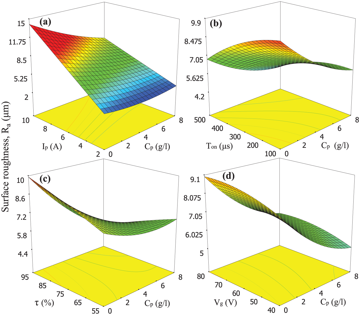
Surface plots: (a) Cp versus Ip, (b) Cp versus Ton, (c) Cp versus τ, and (d) Cp versus Vg for SR using graphite powder.
Surface plots: (a) Cp versus Ip, (b) Cp versus Ton, (c) Cp versus τ, and (d) Cp versus Vg for SCD using aluminum powder.
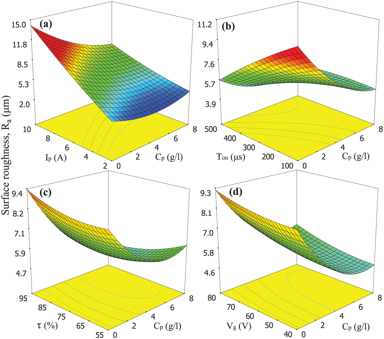
Surface plots: (a) Cp versus Ip, (b) Cp versus Ton, (c) Cp versus τ, and (d) Cp versus Vg for SCD using silicon powder.
Several factors might have contributed to this behavior. First, the higher density of Al powder, compared to graphite powder, prevents it from mixing homogeneously with dielectric. Hence, discharge energy is more uniformly spread among the powders in case of graphite, which allow it to generate tiny and shallow cavities. On the contrary, Al particles have tendency to agglomerate due to Van der Waals’ or electrostatic force when impregnated in dielectric. SR diminished with raise in powder concentration and began to increase at high concentration due to large discharge region, which led to the reduction in energy density to form big diameter, facile cavities on workpiece surface. Excessive particles in electrode gap lead to short circuiting that causes an increase in SR. 19
Surface microhardness
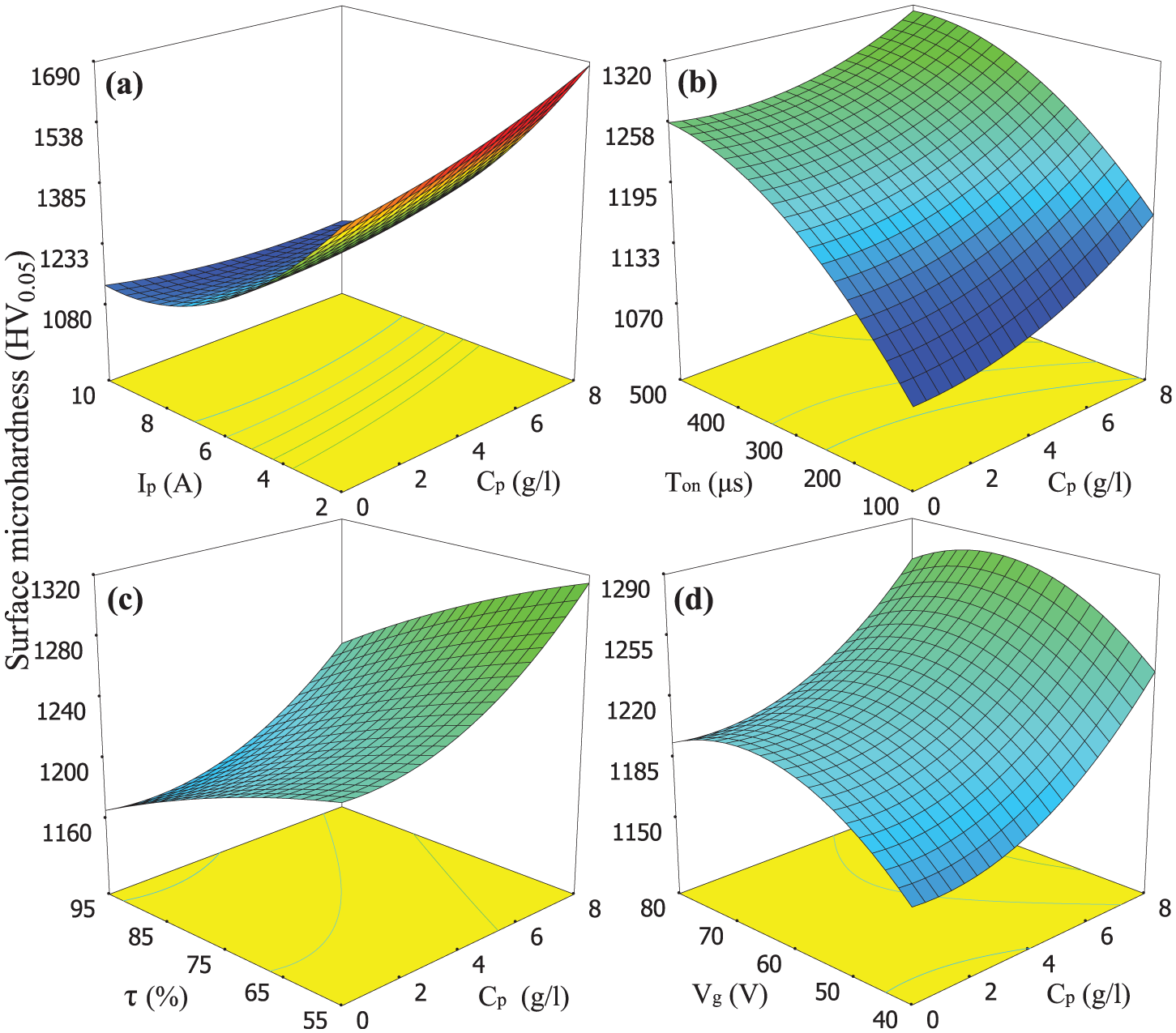
Conducting and semi-conducting powders when mixed with kerosene enhance the ionization in inter-electrode gap. PMEDM using different powders revealed surface hardening of Inconel 625 which was clearly more than that obtained with conventional EDM (with pure dielectric). The possible mechanism behind this interesting phenomena may be explained as follows. The energized charges in electrode gap cause more pyrolysis and breakage of C–H bonds. The abundant number of carbon atoms at workpiece surface leads to the creation of hard metal carbides on its surface. Increase in surface microhardness may also be attributed to the promotion of cuboidal γ’ phase due to transfer of discharge energy to the workpiece. Thus, precipitation of γ’ phase restricts the movement of dislocations and improves the rupture and creep resistance of the material.
Figures 11–13 show the influence of different powders and machining conditions on microhardness. Microhardness clearly increased with peak current due to high energy heating and quenching. Microhardness increased with pulse-on time owing to the increase in thermal energy.
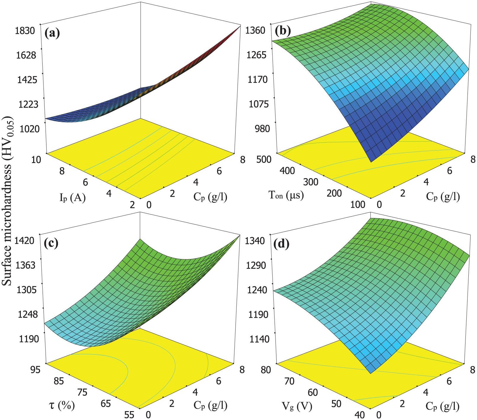
Surface plots: (a) Cp versus Ip, (b) Cp versus Ton, (c) Cp versus τ, and (d) Cp versus Vg for surface microhardness using graphite powder.
Surface plots: (a) Cp versus Ip, (b) Cp versus Ton, (c) Cp versus τ, and (d) Cp versus Vg for surface microhardness using aluminum powder.
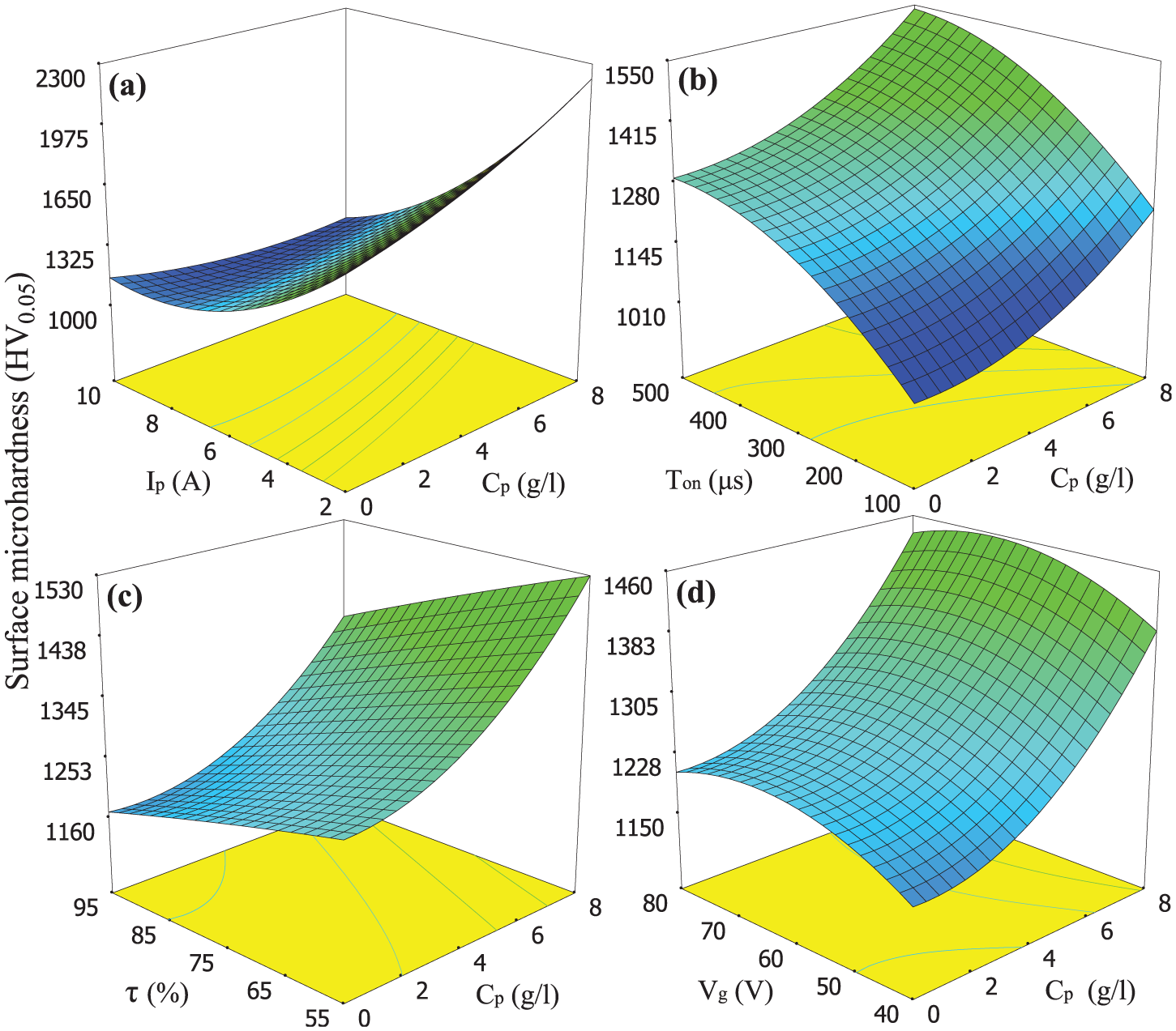
Surface plots: (a) Cp versus Ip, (b) Cp versus Ton, (c) Cp versus τ, and (d) Cp versus Vg for surface microhardness using silicon powder.
Energy density decreases with the increase in pulse-on time and little deposition takes place. Hence, microhardness reduces at high pulse-on time. Increase in duty cycle enhances microhardness due to the enhancement of discharge energy. At high duty cycle values, time available for cooling tends to become very small. Hence, low microhardness values are noticed. Spark energy augments with gap voltage. At large gap voltage, the spark gap becomes very large and energy density diminishes. This results in the reduction in microhardness.
Among the three used powders, Si produced the highest microhardness as less amount of energy is taken away from the sparking zone due to its low thermal conductivity. Availability of high thermal energy and quenching results in the formation of hard workpiece surface. Generation of silicon carbide (SiC) on the machined surface also improves the surface hardness. Interestingly, larger and distinct plates of γ’ phase have already been noted with the sample machined with Si-mixed dielectric. It is followed by Al and graphite in enhancing the surface hardness. Lower electrical resistivity and formation of aluminum carbide (Al4C3) result in harder machined surface with Al-impregnated dielectric compared to graphite-mixed dielectric. Microhardness increased with powder concentration as high amount of particles enter the inter-electrode gap.
Chemical composition
In order to investigate the influence of different powder materials on possible alteration in chemical composition of Inconel 625, EDS analysis was carried out on the machined surface.
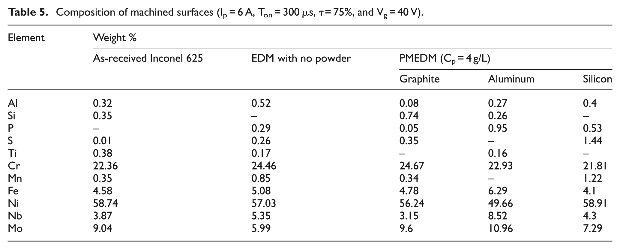
Table 5 shows the chemical composition of as-received Inconel 625 and that after machining the same material using with and without powder-mixed dielectric under the specified machining conditions. After carefully studying Table 5, it is evident that although EDM could not significantly alter chemical composition of Inconel 625, addition of powders resulted in variation in relative content of Nb and Mo at the expense of Ni and Fe. Weight percentage of Mo consistently increased in case of PMEDM. This might be due to the fact that redistribution of thermal energy due to PMEDM was favorable for realignment of elements like Mo to cause solution strengthening and formation of metal carbides. This phenomenon prominently contributed to the enhancement of surface microhardness after PMEDM in comparison with conventional EDM. Rise in content of Nb along with Fe after aluminum-mixed EDM might have promoted formation of δ or laves phase.20,21
Composition of machined surfaces (Ip = 6 A, Ton = 300 µs, τ = 75%, and Vg = 40 V).
After revealing the bulk information of the machined surface after PMEDM, attempt was also made to reveal to extract information from the selective regions. Such results are presented in Figures 14–16. The investigated light gray region (area 1) in Figure 14(a) apparently consists of fcc γ matrix which is solid solution strengthened by Cr and Mo according to the EDS result in Figure 14(b). Interestingly, when the region mainly comprising γ’ precipitates was probed, it was revealed there was a hike in percentage of C, Nb, Mo, Al, and Ti at the expense of Ni and Cr. Area 2, therefore, is logically assumed to consist of δ phase, metal carbides apart from γ’ phase. Suspension of graphite powder to the dielectric was responsible for formation of metal carbides. However, content of Nb was considerably less for the samples machined with aluminum and silicon powders at the specified locations as indicated in Figures 15 and 16. Any trace of carbon could not also be detected. Therefore, it may be inferred that Nb-rich phase was not present in selected point for aluminum-mixed EDMed sample, although it was prevalent at the bulk of the machined surface. Increase in the amount of S and Mn, and Nb after EDM might be ascribed to the possible formation of SO2 and MnO2 at the surface and sub-surface regions.
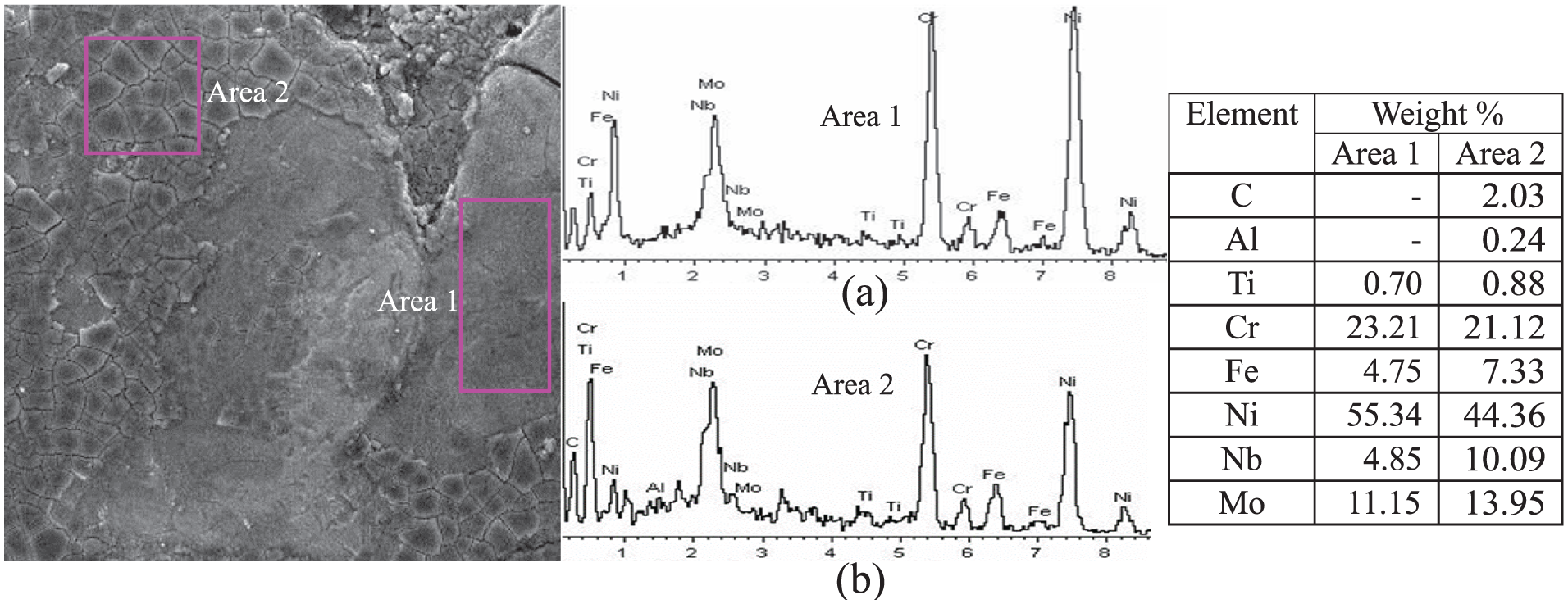
SEM image and EDS results of the sample machined with graphite-mixed dielectric under the condition of Cp = 4 g/L, Ip = 6 A, Ton = 300 µs, τ = 75%, and Vg = 40 V: (a) area 1 and (b) area 2.
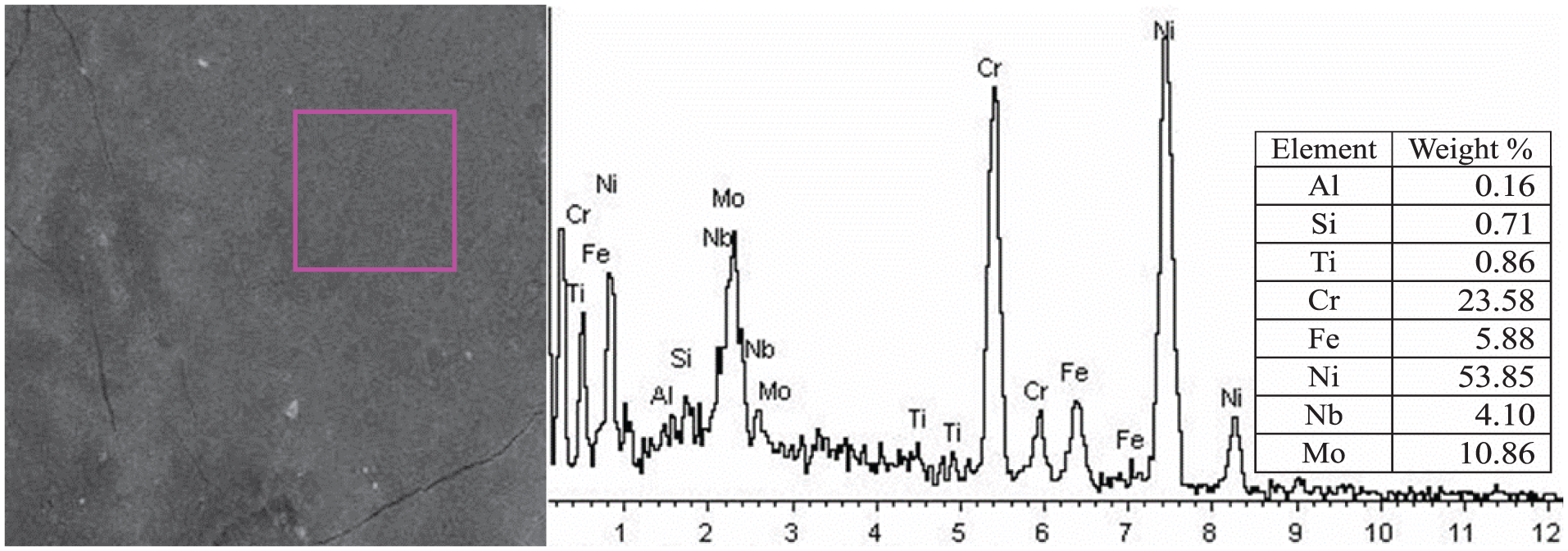
SEM image and EDS results of the sample machined with aluminum-mixed dielectric under the condition of Cp = 4 g/L, Ip = 6 A, Ton = 300 µs, τ = 75%, and Vg = 40 V.
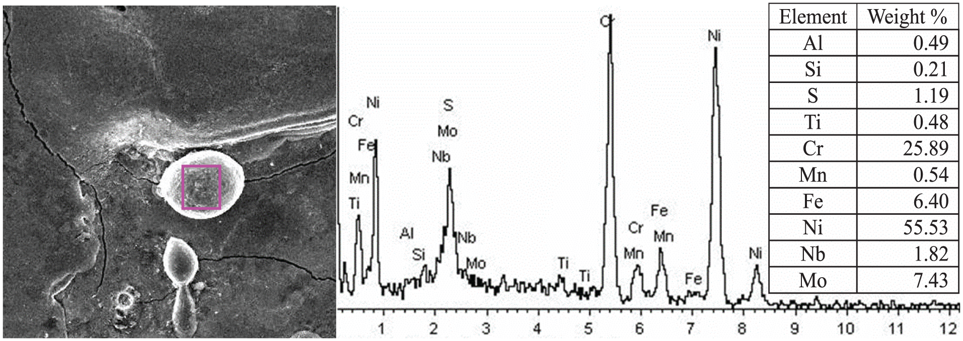
SEM image and EDS results of the sample machined with silicon-mixed dielectric under the condition of Cp = 4 g/L, Ip = 6 A, Ton = 300 µs, τ = 75%, and Vg = 40 V.
Residual stress
High energy sparking in EDM develops extreme temperature differences in the machined surface layers. During rapid cooling process, tensile residual stress develops on the EDMed surface. 22 Cracks are formed when this tensile residual stress exceeds the fracture strength of the material. Residual stress during EDM (without powder) is due to periodic heating and cooling leading to formation of cracks. Thus, crack formation and thermal residual stress generally follow the same trend. However, in PMEDM, a part of thermal induced stress is relieved due to the mechanical abrasive action of the powder particles. The abrasive action increases with the hardness of the particles and if the particles have sharp edges. 23 In this study, silicon particles with higher hardness (Table 3) and sharper edges than other particles produced the least residual stress. Graphite, however, takes away good amount of heat from sparking zone due to its high thermal conductivity and low density (Table 3) forming less number of cracks.
Figure 17 shows the residual stress plots of the machined surfaces under different machining conditions. High tensile residual stress (Figure 17-A) was observed for the sample machined with pure kerosene due to high discharge energy density. The tensile stress got reduced (Figure 17-B and 17-C) with the addition of different powders to the dielectric as the added powder results in low-discharge energy density due to spark gap enlargement.
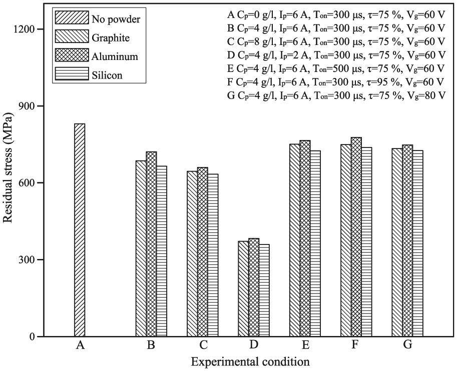
Residual stress with and without powder-mixed dielectric under different conditions.
Little consideration would indicate that tensile residual stress is minimum for silicon powder throughout. Silicon owing to its high heat of fusion and thermal conductivity (Table 3) has the capability to retain heat energy and dissipates it efficiently by virtue of its high thermal conductivity. The mechanical erosive action of silicon particles on the crater ridges also augments the reduction in tensile residual stress. As a consequence, tensile residual stress could be restricted. Although, aluminum also possesses high thermal conductivity, due to its lower heat of fusion, tensile stress is more for silicon and graphite powders in general. Further, agglomeration of aluminum at higher concentration (8 g/L) led to the possibility of arcing. Similarly, under the condition of highest duty cycle (95%), similar condition might have prevailed. Therefore, tensile stress was the highest for aluminum powder under such situations.
The tensile stress also reduced when current reduced from 6 to 2 A (Figure 17-D) due to the reduction in discharge energy. At high pulse-on time of 500 µs the stress declined (Figure 17-E) because of the reduction in energy density due to discharge passage expansion. For the same reason, low tensile residual stress (Figure 17-F) was realized with the increase in duty cycle. A fall in tensile stress was observed (Figure 17-G) with the increase in gap voltage. This is attributed to the reduction in energy density due to the enlargement of discharge column with the gap voltage.
Due to the formation of inter-metallic phases like Ni3Nb, the superior mechanical properties in the form of higher hardness and rupture strength will be achieved. As a result, the machined component would have greater resistance to indentation, crack propagation, and rupture. This would be possible only when surface tensile strength reduces. Decrease in surface residual stress is also manifested in the reduction in surface cracks.
Conclusion
In this research work, the effect of various powders (graphite, aluminum, and silicon) on different surface integrity characteristics was investigated after powder-mixed EDM (PMEDM) of Inconel 625. Comparative evaluation of all the process characteristics was made considering all the three powder materials. Additionally, influence of various process parameters was also investigated. Results clearly demonstrated remarkable improvement in terms of various surface integrity measures for PMEDM compared to EDM without powder additives. The following major conclusions obtained from this work can be drawn:
For all the three powder-suspended dielectrics, larger and shallower cavities were realized compared to conventional EDM due to increased conductivity of dielectric that allows sparking to occur from a long distance.
Conventional EDM resulted in highest number of surface cracks while PMEDM is effectively reduced the same. Graphite is recommended for reducing the number of surface cracks, followed by Si and Al powders.
Si powder is recommended for obtaining fine surface finish followed by Al. Smaller size and the abrasive action of Si powder on crater ridges also enhanced the improvement of surface quality. However, at higher powder concentrations (above 4 g/L), graphite powder yielded better surface finish compared to Al particles.
Si is suggested for obtaining high microhardness of the machined surface followed by aluminum and graphite.
Relative content of nickel was reduced at the expense of Nb and Mo after addition of powders like aluminum and graphite in dielectric during EDM.
Tensile residual strength of the machined surface has declined with the suspension of powder additives in the dielectric. Silicon powder has resulted in least residual stress followed by graphite and aluminum.
Footnotes
Declaration of conflicting interests
The author(s) declared no potential conflicts of interest with respect to the research, authorship, and/or publication of this article.
Funding
The author(s) received no financial support for the research, authorship, and/or publication of this article.