
Abstract
This article presents an experimental investigation of wire cut electro discharge machining of pure titanium. The marvelous characteristics of pure titanium such as its compatibility and noticeable physical, mechanical and biological performances have led to their increased application in various industries especially in seawater pipings, heat exchangers, implants, prosthesis, airframe and aircraft engine parts over the last 50 years. However, due to low thermal conductivity of titanium and their reactivity with cobalt in most tool materials, there are some difficulties in machining titanium and its alloys by conventional machining. On the other hand, unconventional machining processes especially wire cut electro discharge machining are more appropriate techniques for machining difficult-to-machine materials like pure titanium. This research work is mainly focused on microstructure analysis in terms of machining parameters such as pulse on time, pulse off time, peak current, spark gap using energy-dispersive X-ray, scanning electron microscope and X-ray diffraction techniques. The present results reveal that pulse on time and peak current significantly deteriorate the microstructure of machined samples, which produces the deeper, wider overlapping craters, pockmarks, globules of debris and micro-cracks. The microstructure analysis of rough cut surface was based upon the theory of electrical discharge phase and metallurgical physics.
Keywords
Introduction
Pure titanium offers good corrosion resistance in most environments, excluding those containing fluoride ions where it cannot compete with some ceramics, tantalum and various high-nickel alloys. In fluoride-free environments, titanium is cost-effective when competing with high-alloy, corrosion-resistant materials such as Hastelloy. 1 When compared with stainless steel, titanium has a much superior technical performance but would not be selected over commodity products such as ferritic and austenitic stainless steels as it is not cost-effective. Competing in those markets where these stainless steel products fail is difficult as the steel industry has an aggressive product development program. Titanium must be cost-effective when compared with high-performance ferritic, super-austenitic and duplex stainless steels. A number of factors affect the demand for titanium in industrial applications, not the least of which is cost-effectiveness, which depends on the following factors: 2 the cost of titanium sponge and scrap of suitable quality; the value added in melting and primary fabrication, low-cost processing with efficient high-volume mill equipment rather than the current small, batch processing; the value added in component fabrication and the availability of commercial products, including alloys, shapes, sizes and types that are designed for non-aerospace applications and have adequate engineering data for design specifications and effective market development and technical support, including downstream elements such as design assistance, training in fabrication and on-site welding.
It is rare for an application to be satisfied by a single material, and titanium must compete in a fast developing market for advanced materials. Whenever aluminum is technically adequate for an application, it will be preferred to titanium because of its lower density and cost. Polymers have a significant density advantage over titanium, but engineering polymers are expensive and also lack an extensive base of standards and design specifications. 2 The aerospace industry is the single largest market for titanium products. Titanium’s high corrosion resistance is also a valuable characteristic. When exposed to the atmosphere, titanium forms a tight, tenacious oxide film that resists many corrosive materials. Microstructure and mechanical properties in metals are intimately coupled. On a microscopic level, the interaction of crystalline structures in pure titanium and its alloys determines the mechanical properties of that alloy. On a macroscopic level, thermo-mechanical processing manipulates the formation of crystalline phases. The major applications of pure titanium are given as follows: 3
Extensively used for seawater pipings, reactor vessels and heat exchangers;
Orthopedic applications, such as implants and prosthesis;
Airframe and aircraft engine parts;
Marine chemical parts, fish breeding cages, handrails, building, structures and monuments and wheelchairs;
Condenser tubing;
Titanium is used for heart valves;
The Apollo capsules were made largely of pure titanium and many parts of the space shuttle are made of the metal;
The metal is used for the production of engine parts, portable computers, car accessories and sports equipment (golf clubs, tennis rackets, bicycles or underwater sport equipment.
Machinists have developed few methods for commercial machining of pure titanium in manufacturing industries all over the world. Most of the machining work for pure titanium is related to drilling, so twist drilling and vibration-assisted drilling are two conventional machining methods being used in recent times. For other machining operations, special considerations are to be taken care of while machining titanium parts on a machine tool. Titanium and its alloys are very sensitive to changes in cutting speed. Industry generally operates at cutting speeds providing longer tool life. Moreover, because of the bouncy action generated due to low modulus of elasticity of titanium, the rigidity of a machine tool becomes an important consideration. 4 The average unit power requirements for turning or milling of titanium have been found to be much lower than that for high-temperature Ni/Co-based alloys or tool steel grades. As far as the cutting tools are concerned, the straight tungsten carbide (WC) cutting tools, typically C-2 grades, perform best in operations such as turning and face milling, while the high-cobalt, high-speed steels were most applicable in drilling, tapping and end milling. 5 Despite the establishment of effective machining methods using conventional technology, lower tool life and poor surface quality are two major concerns that continue to be associated with the machining of titanium components. Besides this, poor surface integrity of conventionally machined titanium parts is another area where more concentration is required. Nonconventional machining methods like electro discharge machining (EDM) and laser beam machining (LBM) are also used for machining of titanium. EDM with its inherent advantages for machining workpieces with special shape, regardless of material strength or hardness, but also has low machining efficiency as compared to traditional machining process. In addition, the recast layer (RL) with micro-pits and cracks caused by rapid cooling gives both worse surface accuracy and shorter tool life. 6 LBM being a thermal process produces thermal stress and a heat-affected zone (HAZ) in the material. A few studies have reported the use of ultrasonic machining process for machining of pure titanium.7–9 However, the machining productivity has been found to be very low along with higher tool fabrication and operating costs. Much work has been devoted to the study of surface integrity in EDM of common steel alloys, particularly tool and die steels. However, little research has been reported on the effects of wire cut electro discharge machining on the surface characteristics of pure titanium. Specifically, no significant literature has been found by the authors relating to surface integrity of pure titanium after processing with wire electro discharge machining. The novelty of present research work is mainly the investigation of the surface integrity of pure titanium and wire surface topography analyzed through energy-dispersive X-ray, scanning electron microscope and X-ray diffraction techniques. The influence of process conditions on surface topography, RL, HAZ, formation of micro-cracks and debris analysis was considered in the present study. Wire electro discharge machining uses electrothermal mechanisms to cut electrically conductive materials. The material is removed by a series of discrete discharges between the wire electrode and the workpiece in the presence of dielectric fluid, which creates a path for each discharge as the fluid becomes ionized in the gap. The area where discharge takes place is heated to extremely 7, so that the surface is melted and removed. The removed particles are flushed away by the flowing dielectric fluids. The wires for wire electro discharge machining are made of brass, copper, tungsten and molybdenum (0.05–0.3 mm) in diameter, which is capable to achieve very small corner radii. Zinc- or brass-coated wires are also used extensively in this process. 10 The wire used in wire electro discharge machining process should possess high tensile strength and good electrical conductivity. Wire electro discharge machining process is usually used in conjunction with computer numerical control (CNC) and will work only when a part is to be cut completely through. The melting temperature of the parts to be machined is an important parameter for this process rather than strength or hardness. The surface quality and material removal rate (MRR) of the machined surface by wire electro discharge machining will depend on different machining parameters such as applied peak current and wire materials. Wire electro discharge machining process is commonly conducted on submerged condition in a tank fully filled with dielectric fluid. Hewidy et al. 11 modeled the machining parameters of WEDM of Inconel-601 using response surface methodology (RSM). Volumetric metal removal rate generally increased with the increase in peak current value and water pressure. Kumar et al. 12 explored the study on WEDM in machining of commercially pure titanium (Grade-2). The parameters such as pulse on time, pulse off time, peak current, spark gap set voltage, wire feed and wire tension were varied to investigate their effects on the cutting rate, gap current and surface roughness of the machined specimens. Kung and Chiang 13 studied the behavior of WEDM of aluminum oxide-based ceramics. The effects of machining parameters on MRR and surface roughness were evaluated. Huang and Liao 14 investigated the microstructure analysis of martensitic steel fine surface by WEDM. The microstructure of finished surface has been analyzed by EDX, SEM and transmission electron microscope (TEM). Hascalik and Caydas 15 experimentally investigated the machining characteristic of AISI D5 tool steel in WEDM process. The study was found that the intensity of process energy does affect the amount of RL and surface roughness as well as micro-cracking.
From the literature review, it was concluded that limited work has been reported on surface texture of pure titanium. The most of research work was mainly focused on the modeling and optimization of process parameters of wire electro discharge machining. In this research work, wire electro discharge machining surfaces are employed to analyze using energy-dispersive X-ray analysis, scanning electron microscope and X-ray diffraction techniques.
Experimental procedure
Work material and machine setup
The experiments were performed on a four-axis CNC type wire electro discharge machining (Electronica India, model Sprintcut-734), as shown in Figure 1(a). The parameters kept constant during machining are shown in Table 1. The chemical composition of work material taken for experimentation was C: 0.10%, N: 0.03%, O2: 0.25%, H2: 0.015%, Fe: 0.30% and Ti: 99.03%. Figure 1(b) and (c) shows the machine setup and job profile during machining. The CNC program for machining was generated using ELAPT software. Table 2 presents the factors and their levels. The factors and levels of the present study have been selected on the basis of pilot experimentation using one-factor-at-a-time approach method. According to experimental design plan as shown in Table 3, parameters such as pulse on time, pulse off time, peak current and spark gap voltage were varied to explore their effect on surface integrity of pure titanium.
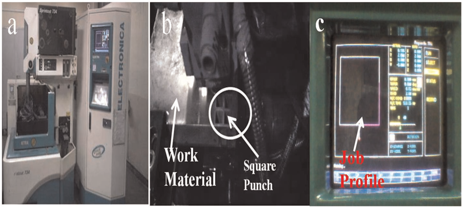
Job profile and experimental setup of wire electro discharge machining machine tool: (a) four-axis wire electro discharge machining CNC type, Electronica India, model Sprintcut-734 machine tool, (b) square punch produced after wire electro discharge machining and (c) job profile during machining.
Wire electro discharge machining fixed operating conditions.
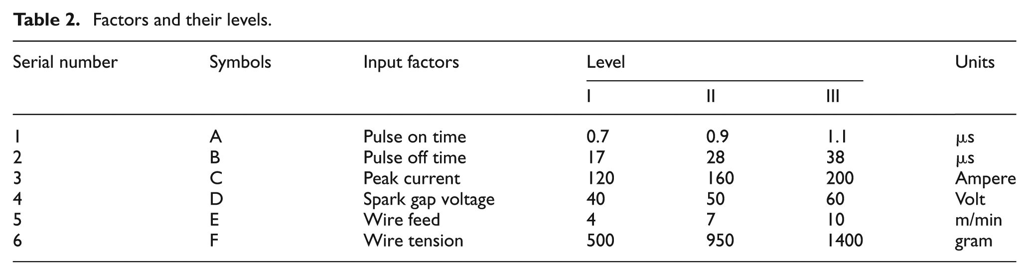
Factors and their levels.
Experimental design plan.
Surface integrity analysis equipment
In this study, the surface integrity was analyzed using SEM (JSM-6610LV; JEOL, Tokyo, Japan), which was integrated with an EDX spectrometer. Before SEM, the machined samples were etched with Kroll’s reagent (2 mL hydrofluoric acid, 10 mL nitric acid and 88 mL distilled water). The samples were also cleaned with acetone ((CH3)2CO). The EDX spectrometer was used to analyze the surface of machined samples. The XRD analysis was used to investigate the significant material transfer from the dielectric as well as tool electrode on the work surface either in free form and/or in compound form.
Experimental results and discussion
Surface topography
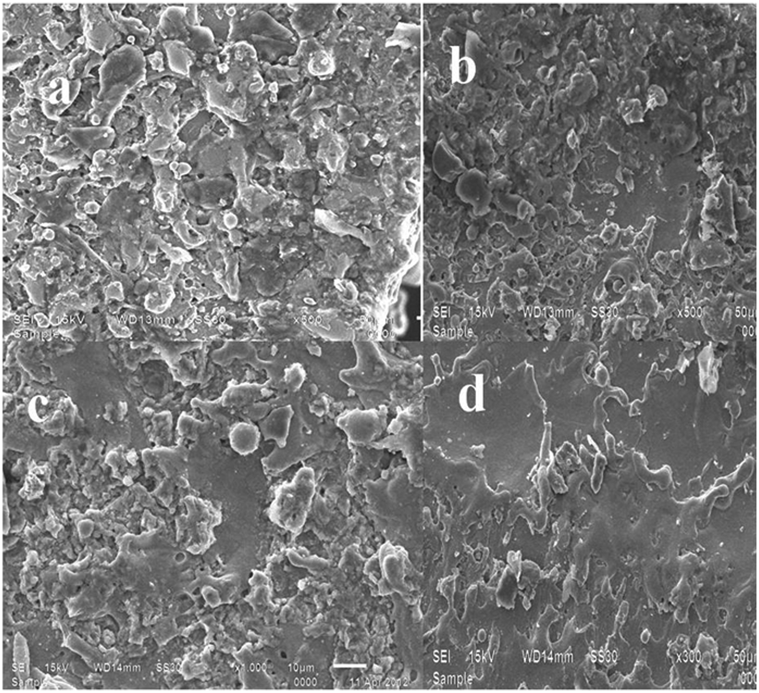
Surface topography is at present receiving attention in the engineering industry, since it is well established that there exists some relationship between the surface properties and reasons of failure modes of the components and service performance. The fatigue strength of the components is seriously affected by the surface roughness, that is, as the roughness increases, the fatigue life decreases. Moreover, to face the global competition, it is desirable in the industry to reduce the cost and improve the quality. Better surface morphology helps to improve the precision and quality of conformance of the product. Wire electro discharge machining process is very demanding, but the mechanism of process is complex and far from completely understood. The aim of this study is to investigate the surface topography of wire electro discharge machining surfaces and explores possible ways to adjust its parameters to achieve better surface roughness. A RSM is applied for the analysis of surface topography with pulse on time, pulse off time, peak current, spark gap voltage, wire feed and wire tension as input parameters. As shown in Figure 2(a)–(d), SEM micrographs revealed that the surfaces have complex appearance with shallow craters, spherical particles, melt drops, globules of debris, pockmarks, micro-cracks and voids due to the high heat energy released by discharges and subsequently cooling. The spherical particles are molten metals that are expelled randomly during the discharge and then solidified and attached to the surface. SEM micrographs of pure titanium at various levels of parameters as mentioned along with the micrographs are presented to qualitatively access the surface topography. The pulse on time (1.1 µs) and peak current (200 A) were observed as the most significant parameters affecting the surface properties. A previous study reported by Hascalik and Caydas 16 has shown that the most significant parameters are pulse on time and peak current for the surface integrity of pure titanium, which leads to deteriorate the surface texture. When pulse on time was increased, the surface texture of the machined surface is composed of varying sizes of deep crater rims. These deep and overlapping crater rims were formed due to successive electrical discharges, intense heat and local melting or evaporization of work material. It was observed that low pulse off time (17 µs) and high pulse on time (0.9 µs) may result in electrical sparks, which generate smaller crater rims on the work surface, as shown in Figure 3(a)–(d). Some of the molten material produced by the discharge was carried away by the deionized water. The remaining melts and resolidifies to form lumps of debris, as shown in Figure 4(a)–(d), due to high discharge energy and high pulsed current (200 A), which caused frequent cracking of dielectric fluid, causing more melt expulsions and larger tensile stresses. These effects were turned in poor surface finish (3.22 µm). At higher peak current (160 A), the impact of discharge energy on the surface of workpiece becomes greater, and thus, resulting erosion leads to the increase in deterioration of surface roughness. A shown in Figure 5, some titanium particles are protruding and completely dislodged from the surface, which may happen at higher pulse on time (0.9 µs) and peak current (160 A). Some spherical shape particles and thermal cracks were observed due to surface tension of molten material. Matt surface with many fine nodules was also observed. These nodules were observed from the solidification of molten or vaporized titanium particles during machining. Spherical shape of the nodules revealed that the surface energy is minimized during solidification. As shown in Figure 6(a)–(d), WEDM surfaces may also have macro-ridges and valleys, which were formed by melted material. This melted material was blasted out of the surface by the discharge pressure and subsequently quickly reached solidification temperature by being cooled by the surrounding dielectric fluid. As shown in Figure 7(a)–(d), less number of craters and no micro-cracks were formed due to lower peak current (120 A), pulse on time (0.7 µs), higher pulse off time (28 µs) and higher spark gap voltage (60 V). Due to lower peak current and pulse on time, the machined surface is impinged with less electrical discharge and may result in improved surface roughness. High peak current (200 A) and low pulse off time (17 µs) increased the debris in the spark gap, which leads to abnormal arcing. The abnormal arcing decreased discharge rate and the MRR. 17 Also abnormal arcing reduced the dielectric strength resulting in wire breakage. It was found that on decreasing the spark gap voltage, the wire speed increases, which leads to increase the MRR. The present study revealed that higher MRR can achieve at the lowest spark gap voltage (40 V), pulse off time (17 µs) and high peak current (200 A). Due to low peak current and pulse on time, the work surface is impinged with less intensive discharge. The percent contributions of various factors have been shown in Figure 8(a). The percentage contribution of various parameters has been found to be the following: pulse on time = 42.31%, pulse off time = 13.85%, peak current = 36.92%, spark gap voltage = 4.62% and error = 2.31%. In order to obtain optimal surface roughness and MRR during WEDM of pure titanium, the optimum parameter combination obtained is pulse on time = 0.7 µs, pulse off time = 28 µs, peak current = 160 A, spark gap voltage = 50 V, wire feed = 7 m/min and wire tension = 980 g.
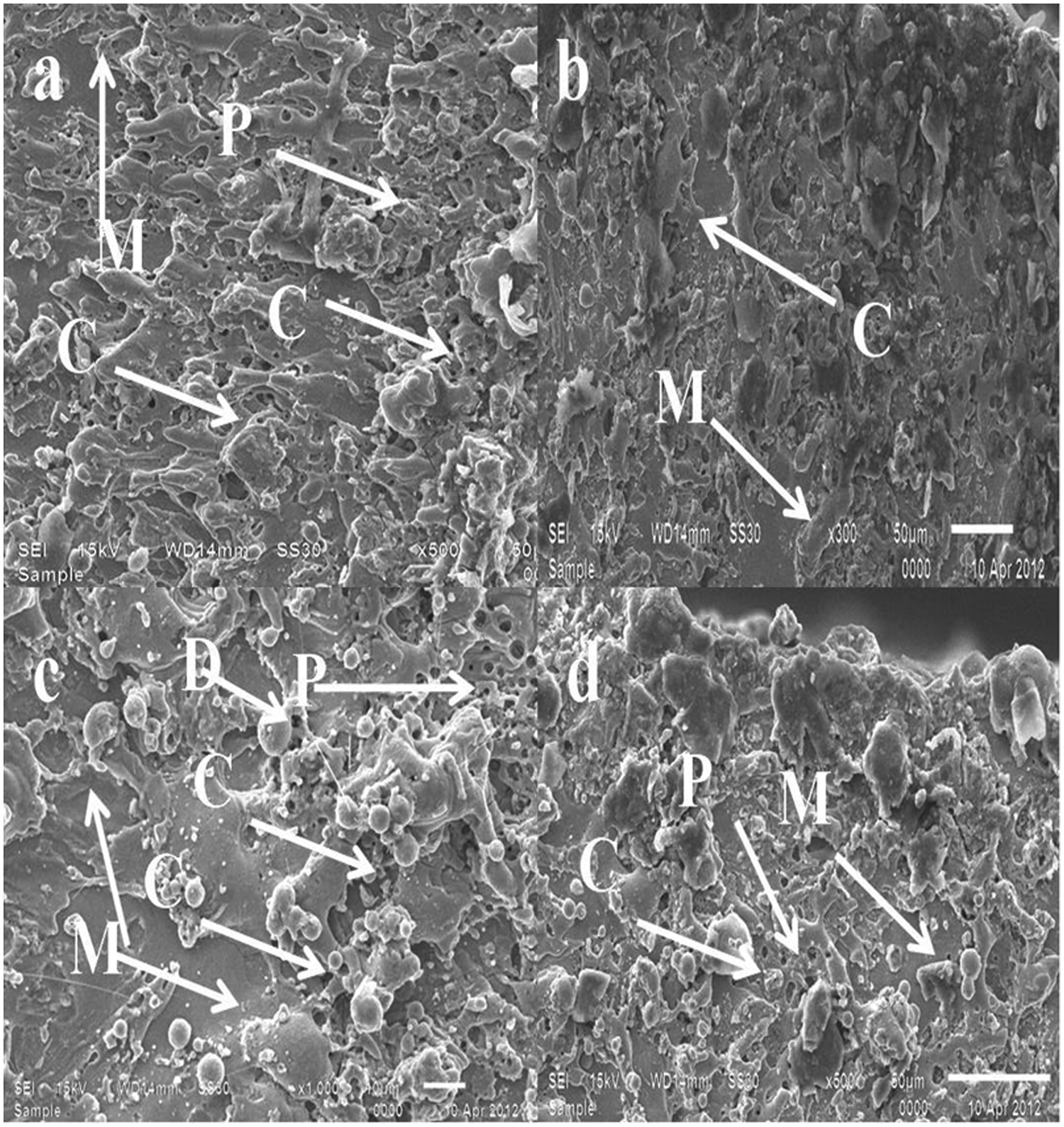
SEM micrographs observed with C = craters, P = pockmarks, D = debris, M = matt surface due to higher pulse on time and peak current (pulse on time = 1.1 µs; pulse off time = 28 µs; peak current = 200 A; Ra = 3.22, 2.93, 2.68 and 2.55 µm).
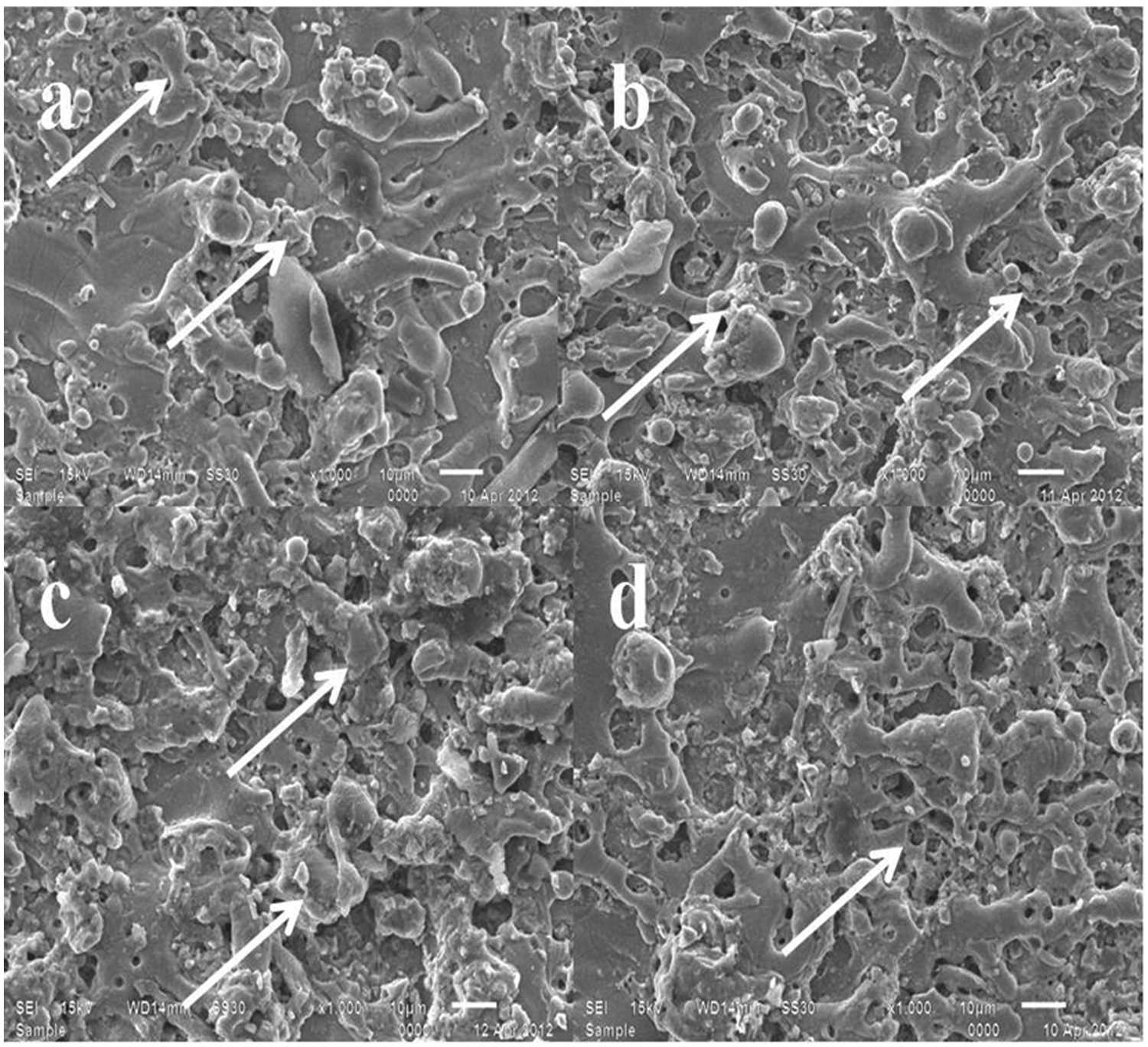
SEM micrograph of varying sizes of crater rims at higher pulse on time and peak current (pulse on time = 0.9 µs, pulse off time = 17 µs and peak current = 160 A).
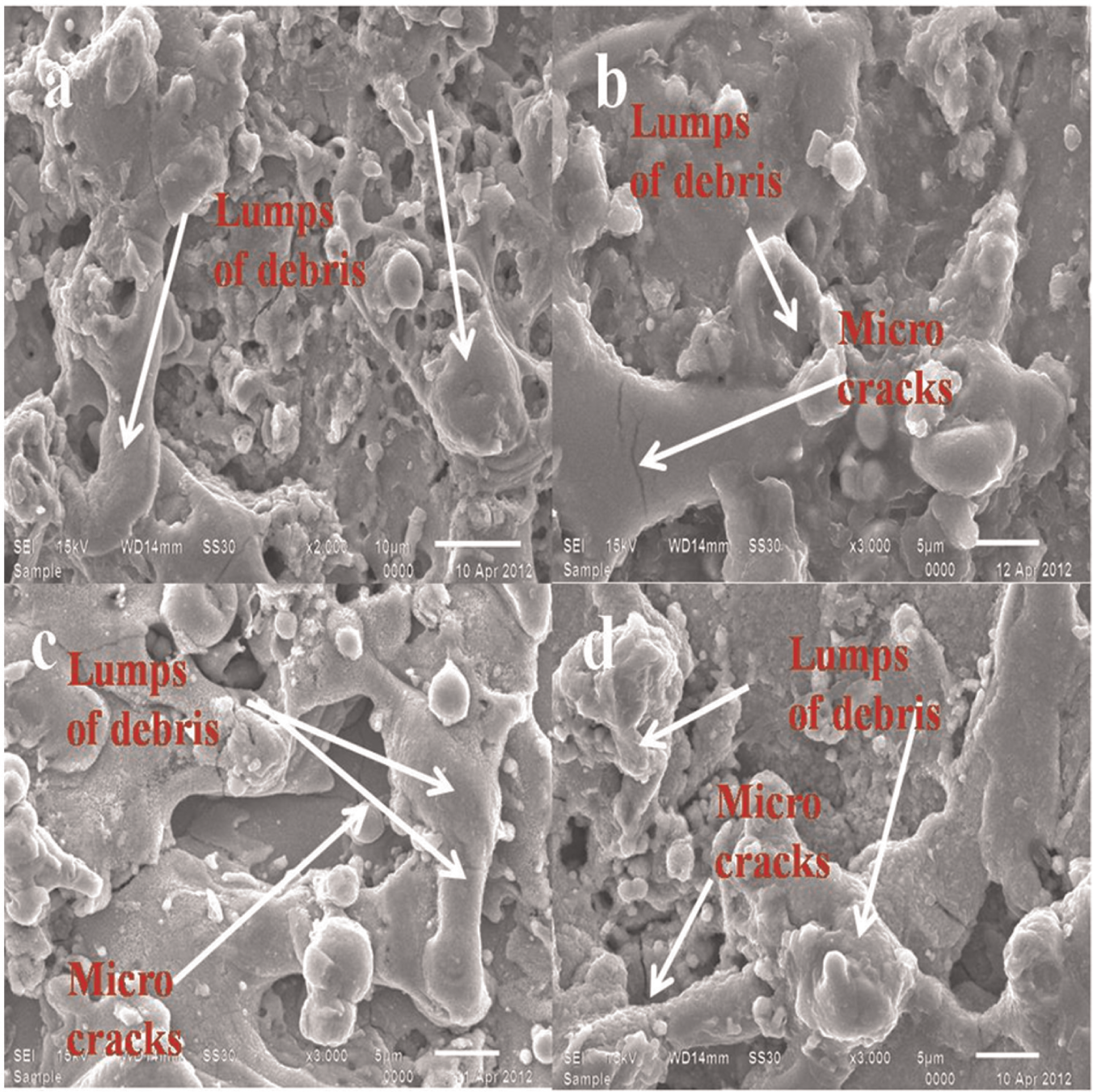
SEM micrograph of melted and resolidified lumps of debris with few micro-cracks at high pulse on time (1.1 µs) and peak current (200 A).
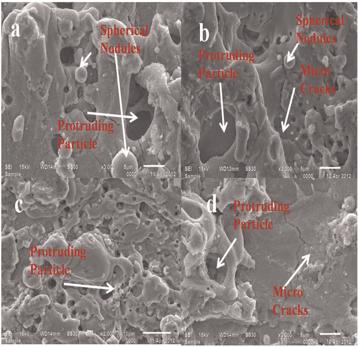
SEM micrograph of protruding titanium particles, micro-cracks and spherical nodules at pulse on time = 0.9 µs, pulse off time = 28 µs, peak current = 160 A and spark gap voltage = 50 V.
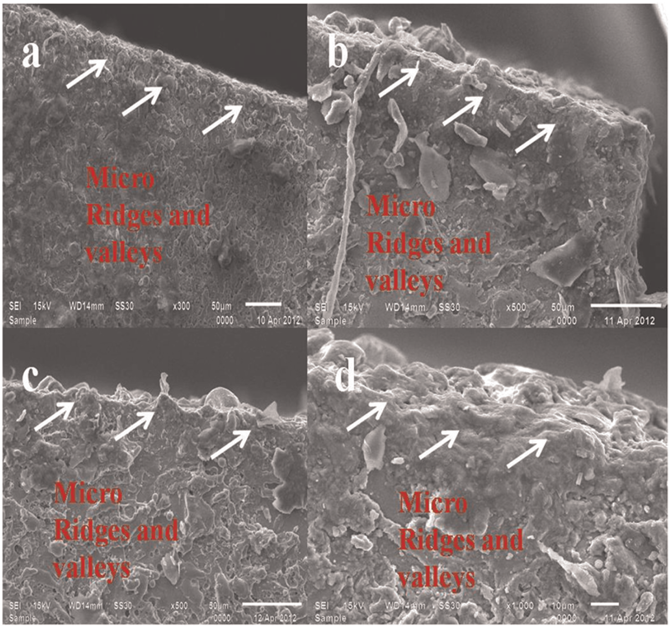
SEM micrographs of macro-ridges and valleys.
SEM micrographs with less number of craters, and no cracks were formed at lower peak current and pulse on time (pulse on time = 0.7 µs, pulse off time = 28 µs, peak current = 160 A and spark gap voltage = 60 V).
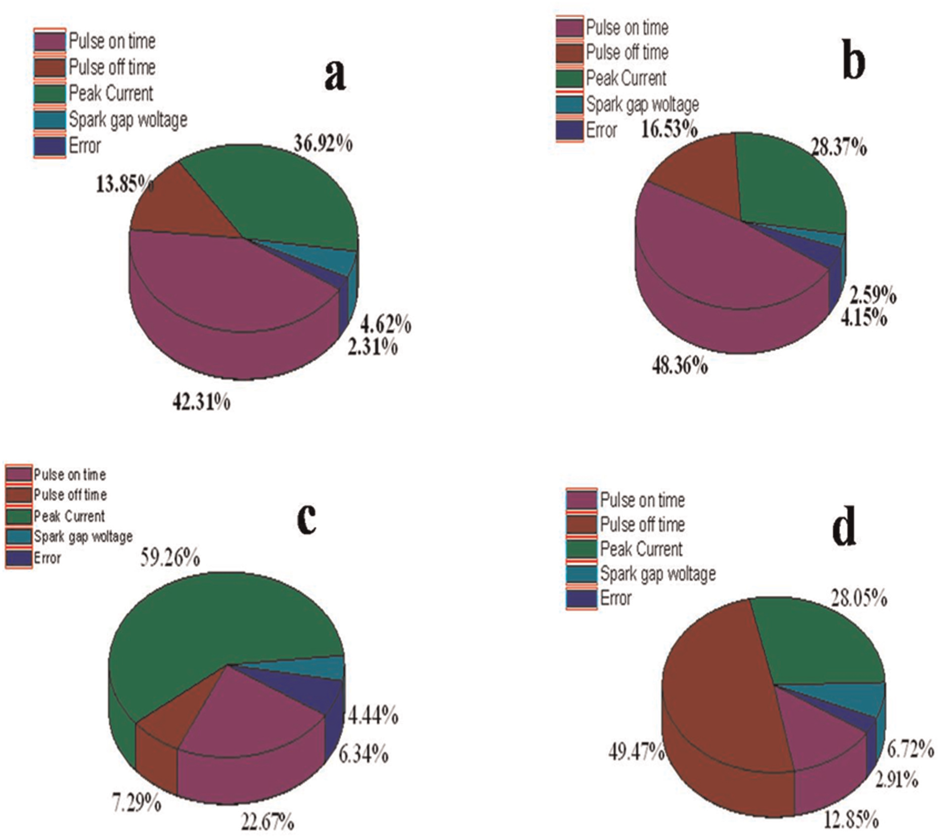
Percentage contributions of most significant parameters on surface integrity: (a) surface topography, (b) recast layer thickness, (c) surface crack size density and (d) wire wear topography.
HAZ and RL
The surface integrity of titanium samples was greatly altered by thermally affected layers, that is, HAZ and RL. Thermally affected layers are formed in subsurface when producing machined surface by WEDM. Below the RL, there is HAZ. A HAZ was formed due to rapid heating and quenching cycles of WEDM process. 18 For the work material and tool electrode, elements melted and resolidified near the HAZ. It is observed in SEM cross section micrographs (Figure 9(a)–(d)). The HAZ of pure titanium consists of large α phase with amounts of 2%−4% β phase, which was observed at α grain boundary. Thermal residual stresses, α grain boundary weakening and some cracks were developed near this zone. At high peak current, a large amount of discharge heat was generated and further absorbed by dielectric medium and work material surface. The discharge heat helps in melting and vaporizing the work material. The residual of spherical nodules in free or compound form was observed near the HAZ. These nodules were developed due to thermal influence and surface tension. These spherical nodules were formed due to higher heat content and rapid cooling, which may lead to martensite α structure in material. The crystal structure of α martensite was intermediate between α phase (hexagonal close packed (HCP)) and β phase structure, which is called body-centered cubic (BCC) crystal stucture. 19 The RL was observed at the cross section of the WEDM surface. The RL is defined as the material melted by electrical discharge and resolidified on the work surface without being ejected nor removed by dielectric fluid. 20 It is very difficult to remove, and its appearance is observed through a SEM at different levels of magnification. The RL thickness was changed due to superficial hardening of the work material by the discharge heat of electrical spark. The intensity of spark depends on peak current, pulse on time and pulse off time. The thickness of RL of WEDM surface was increased due to increase of peak current, pulse on time and decrease of pulse off time, as observed in Figure 10(a)–(d). Due to increase of pulse on time and peak current, the melting of isothermals becomes more intense, which further penetrates into base metal, and the result extends the thickness of RL. It is clear that RLs appear as nonuniform and have wave-like pattern. Carbon is mostly transferred from work material due to high discharge energy and deposited on the machined surface as titanium carbide. The titanium carbide formation was observed through XRD analysis. With regard to RL thickness analysis, the percentage contribution of significant parameters is shown in Figure 8(b). The percentage contribution of various parameters has been found to be the following: pulse on time = 48.36%, pulse off time = 16.53%, peak current = 28.37%, spark gap voltage = 2.59% and error = 4.15%.
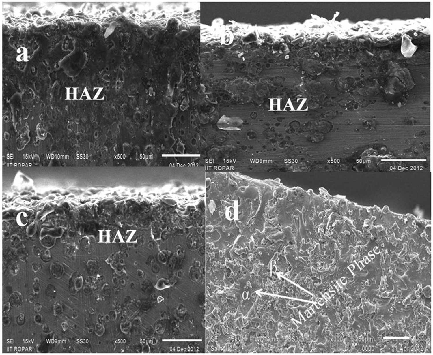
Cross-sectional SEM micrographs of heat-affected zone (HAZ) and α–β martensite phase.
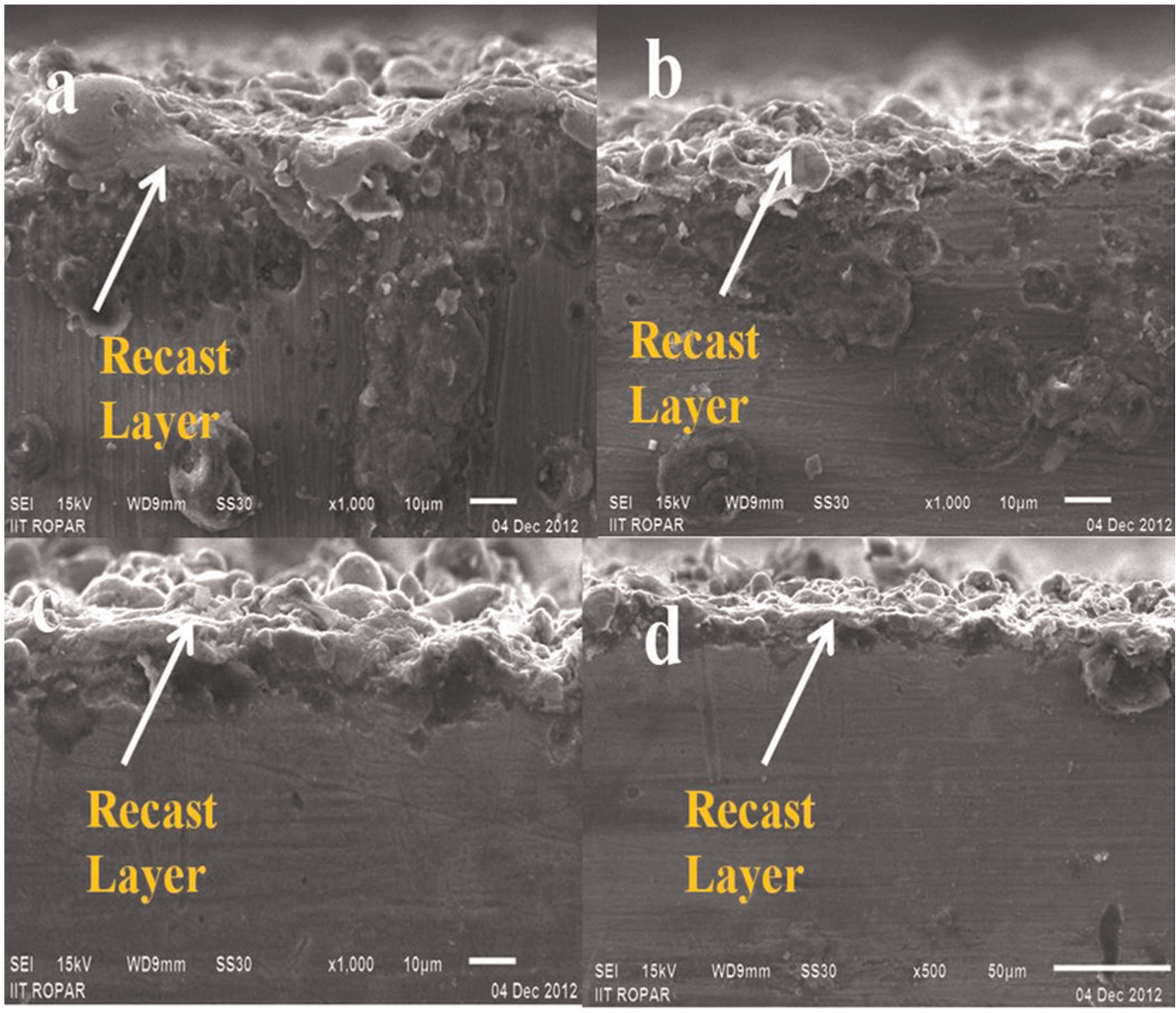
Cross-sectional SEM micrographs of recast layer of WEDM samples: (a) Ton = 0.7 µs, Toff = 38 µs and Ip = 120 A; (b) Ton = 0.9 µs, Toff = 28 µs and Ip = 160 A; (c) Ton = 0.9 µs, Toff = 17 µs and Ip = 160 A and (d) Ton = 1.1 µs, Toff = 28 µs and Ip = 160 A.
Micro-crack formation
The crack formation was usually associated with the development of high thermal stresses, which exceed the fracture strength, as well as with plastic deformation. In addition, the formation of micro-cracks is not only influenced by the setting of machining parameters but also depended on several material properties such as tensile strength, thermal conductivity, thermal expansion coefficient and Young modulus. 21 In order to examine the subsurface cracks of machined samples by WEDM, it is indicated that the material should be amorphous either in free form and/or in compound form. The formation of micro-cracks is generally accompanied by rapid cooling and heating by dielectric fluid. The heating and cooling process was increasing the yield stress, and the material plastically deformed during heating that build up the tensile stresses, which leads to crack formation. The crack distribution on the surface was observed by evaluating the crack density and mean free path of the cracks. Since it is not easy to compute the surface cracking in terms of a judgment of the width, length or the depth of crack, or even by the amount of cracking, this research defines a “surface crack size density,” that is, the total length of cracks (µm) in unit area (µm2) to evaluate the severity of cracking. Observation of these results showed that surface crack size density varies from 0.0053 to 0.0084 µm/µm2 by increasing pulse on time. On the other hand, due to increase of peak current, the surface crack size density varies from 0.014 to 0.019 µm/µm2. The surface crack densities at various peak current and pulse on time were observed in Figure 11. It is observed from Figure 12(a)–(f) that the cracks were developed due to high pulse on time (1.1 µs) and peak current (200 A). The increase of pulse on time and peak current leads to intense heat conditions on the workpiece causing surface cracks to develop on the material. Wider surface cracks were observed due to free path of debris, and they also penetrate more deeply into original material. Overall, the results show that the surface cracks were developed by increasing pulse on time and peak current. With regard to surface crack size density analysis, the percentage contribution of significant parameters is shown in Figure 8(c). The percentage contribution of various parameters has been found to be the following: pulse on time = 22.67%, pulse off time = 7.29%, peak current = 59.26%, spark gap voltage = 6.34% and error = 4.4%. The study observed no formation of surface cracks if machining is carried out according to the machining conditions pertaining to experiment numbers 3, 11, 16 and 19, as shown in Figure 7.
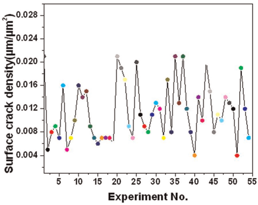
Experiment number versus surface crack size density.
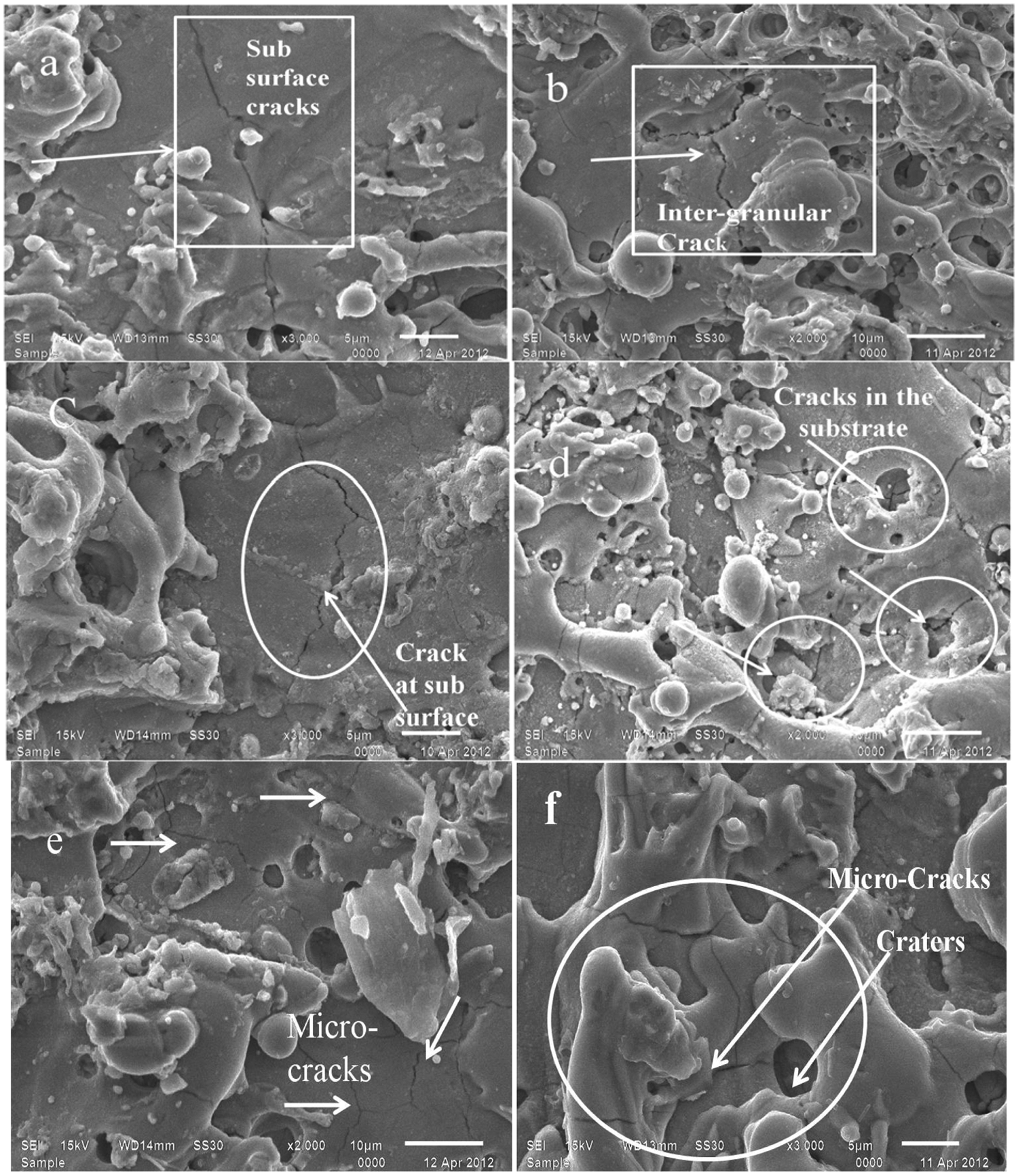
SEM micrographs of micro-cracks observed at (a) Ton = 0.7 µs, Ip = 120 A; (b) Ton = 0.9 µs, Ip = 160 A; (c) Ton = 0.9 µs, Ip = 160 A; (d) Ton = 1.1 µs, Ip = 160 A; (e) Ton = 1.1 µs, Ip = 200 A and (f) Ton = 1.1 µs, Ip = 200 A.
Penetrating micro-cracks in the subsurface
The path followed by the penetrating micro-cracks is so remarkable that they have a trend to follow the temperature isotherms in the solid state at high pulse on time (1.1 µs), low pulse off time (17 µs) and high peak current (200 A) that leads to formation of corresponding cracks, as shown in Figure 13(a)–(d). This can be attributed to thermal action of electric sparks and extreme temperature gradients that occur at the work surface. With increasing pulse on time, penetrating subsurface micro-cracks, craters rims and irregularities is also increased. When pulse on time is increased, the amount of thermal energy, which is transferred to the subsurface of sample as a result of more material, is melted that causes increase of immersed volume of molten material in dielectric fluid and in the spark gap. On the other hand, due to low pulse off time during experiments, there is not enough time for proper cleaning of immersed debris and pollution in gap distance, produced by discharges and leads to unstable conditions of electrical discharge and also occurrence of more arcs in gap distance.
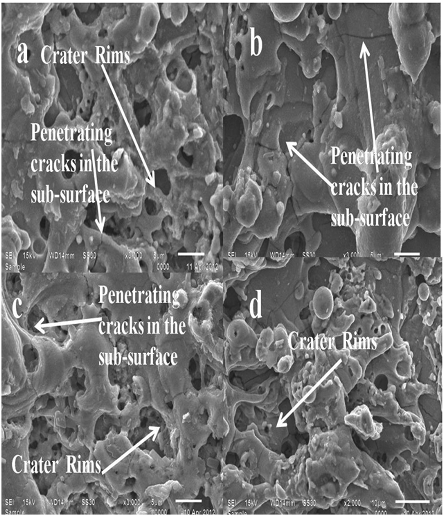
SEM micrographs penetrating micro-cracks in the subsurface.
Comparison of surface integrity between steel and pure titanium
From the application point of view, WEDM is more suitable candidate for machining of pure titanium as compared to machining of other materials such as steel, as steel can be easily machined using conventional machining. A detailed comparison of surface integrity of pure titanium (in the present study) and other materials (such as steel) as reported by other researchers in the literature was difficult to make because all these studies have been reported to make use of different WEDM setups involving different ranges of machining parameters. However, a comparison of surface integrity for pure titanium and steel is done and is presented in Table 4. From Table 4 and literature survey, it was observed that the published work on the EDM surface characteristics of steel and its alloys is reasonably extensive. Furthermore, the research work have been incorporated with multi-objective optimization and modeling activity of electrical parameters.
A comparison of wire cut EDM surface integrity in steel and pure titanium.

Wire surface topography
In present study, two types of wire rupture were observed. One is due to high peak current and other is due to increase of spark frequency. Figure 14(a)–(d) shows the micrographs of worn wire electrode. The different craters and residuals of debris adhered to the surface of wire electrode. This may be due to the melting and resolidification of titanium and electrode elements migrated after WEDM. The migration of copper to the surface of work material during machining with WEDM may improve the lubricity of the titanium part. From EDX analysis, it was observed that a significant proportion of Cu is transferred from the wire electrode to the work surface. 34 The increase of peak current leads to generation of higher discharge energy in the spark gap. Hence, it may result in increase of wear of wire electrode surface. In this research, pulse on time, pulse off time and peak current are identified as the most significant machining parameters for wire breakage as response. The wire breakage probability increases when pulse on time increases and pulse off time decreases simultaneously. To maximize the efficiency of cutting pure titanium material by WEDM, the wire breakage during cutting process should be avoided in addition to increased discharge energy. From these results, the optimum setting parameters can be adjusted accordingly in order to minimize the wire breakage frequency (pulse on time = 0.9 µs, pulse off time = 28 µs and peak current = 160 A) during WEDM of pure titanium. This range of parameters can be used to optimize the WEDM parameters for smooth cutting.
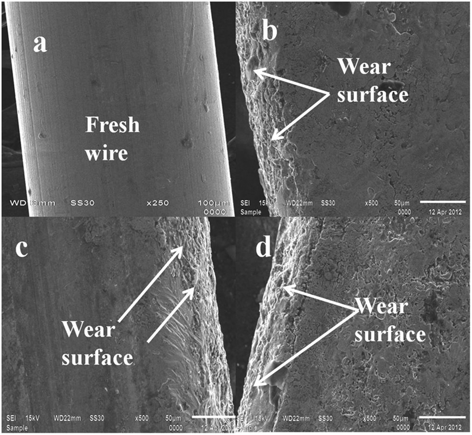
SEM micrographs (250× and 500×) of the machined wire electrode surface for machining at (a) fresh wire; (b) Ton = 0.9 µs, Ip = 160 A; (c) Ton = 0.9 µs, Ip = 160 A and (d) Ton = 1.1 µs, Ip = 160 A.
EDX analysis
The compositions of WEDM samples were detected through EDX. EDX analysis is the technique that is used to identify the elemental composition of the machined samples. The output of an EDX technique is a plot of how frequently an X-ray is received for each energy level. An EDX spectrum normally displays peaks corresponding to the energy levels for which the most X-rays had been received. Each of these peaks is unique to an atom and therefore corresponds to a single element. The higher a peak in a spectrum, the more concentrated the element is in the specimen. Figure 15(a)–(d) shows the EDX of affected surfaces, which are obtained by accelerating voltage of 3 kV. Through EDX analysis, the residuals of copper and zinc were also detected in the machined samples. It may be due to the melting, evaporation and resolidification of the brass wire electrode and may result in transfer to the work material, as shown in Figure 16. The presence of oxygen in the titanium probably was due to oxidation as a result of high temperature involved in the process. Although EDX result showed that carbon and oxygen also existed in the titanium, these elements were observed due to the fact that dielectric fluid with debris normally contains carbon and oxygen.
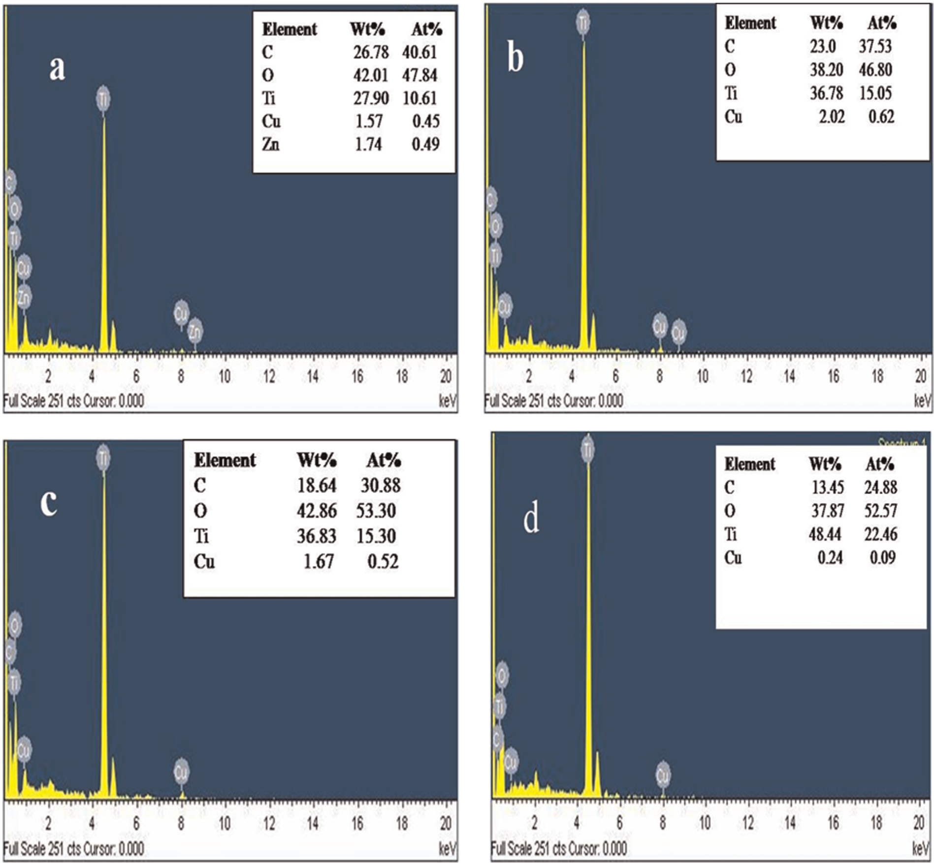
EDX analysis of pure titanium after wire cut EDM.
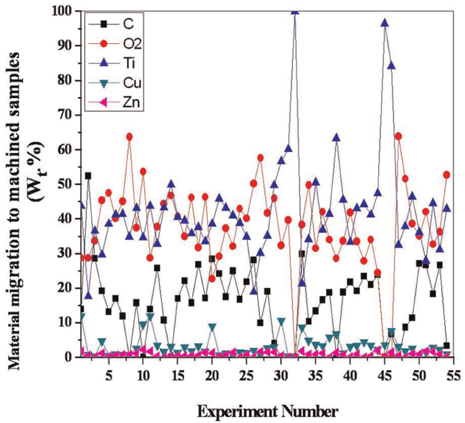
EDX analysis of migrated elements at different experiment numbers versus atomic weight percentage.
XRD analysis
The XRD pattern analysis confirms the migration of tool elements (anode), dielectric fluid elements were migrated to the work surface, and they formed into different compounds as titanium dioxide (rutile) (TiO2), (TiO0.325), Ti2O3, ilmenite (Fe2Ti4O), copper titanium dioxide (Cu3TiO4), zinc titanium carbide (Ti3ZnC), titanium zinc carbide (Zn2Ti4C) and titanium carbide (TiC). They were observed on the machined surface as a free form or combined form, as shown in Figure 17(a)–(f). The phases were identified in the form of peaks at 2θ scale values, that is, 35.45, 45.67, 65.70, 85.07 and 105.69 (Cu Kα), respectively. Pure titanium has found little use in mechanical engineering applications because of their poor tribological characteristics such as poor abrasive wear resistance, poor fretting behavior and high coefficient of friction. The friction problem is related to the crystal structure and reactivity of pure titanium and can be largely overcome by changing the nature of the surface so that the surface is no longer titanium, but a hard compound of titanium. For such purpose, normally thermochemical treatments are applied. However, as observed from the present investigation, use of WEDM as the processing technique yields the formation of harder compounds of titanium on the surface of the workpiece, which might improve the tribological characteristics of processed titanium. 35 The formation of surface oxide, rutile (TiO2), as observed from the XRD analysis may enable the titanium part to develop optimum wear characteristics. 36 The crystal structure of pure titanium at room temperature was HCP. This phase is designated as “α.” The crystalline structure of Ti is dependent on temperature. At standard pressure, above 885 °C, the stable phase for pure titanium is a BCC phase, called β.35,36 The α phase grows into the β matrix when the molten titanium rapidly cooled by dielectric from high temperatures to temperatures below the β transus temperature. The β transus is the temperature that separates the phase stability of β and α phases in titanium. The β→α phase transformation is signaled by the growth of α“laths,” or thin and flat crystalline structures. β-stabilizing elements were classified as either isomorphous (or monotectoid) β stabilizers or eutectoid β stabilizers. Isomorphous β stabilizers share the BCC crystalline structure with β Ti. The elements like C, N, O2, H2 and Fe are eutectoid β stabilizers and thus have a eutectoid reaction with Ti. They exhibit low solubility in α Ti and decrease the β transus temperature. The amorphous structure develops the cracks due to rapid cooling. 22 In this case, the HCP α phase exhibits a lamellar (or lath-like) morphology (long, thin structures). The β phase coexists with the α in “ribs” between laths. The darker, globular regions are the α phase, while the lighter “ribs” between globs are regions of β Ti. The β phase of titanium transforms to the α phase when the molten material is cooled below the β transus temperature. This transformation is facilitated by the Burgers orientation relationship between the two phases. The formation of α laths is a consequence of the α→β phase transformation via the Burgers orientation relationship.
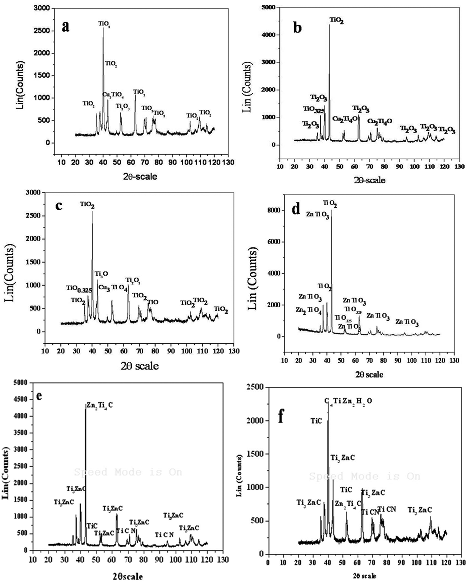
XRD phase pattern analysis of the machined surface.
Conclusion
In the present study, experimental investigation on surface integrity of pure titanium after WEDM was analyzed. There are mainly three significant parameters that were identified, that is, pulse on time, pulse off time and peak current, which effect the surface integrity of pure titanium. Finally, it can be concluded that
The surface integrity was analyzed using SEM. It was observed that pulse on time, pulse off time and peak current deteriorate the integrity of machined samples, which produces the deeper and wider overlapping craters, pockmarks, globules of debris and micro-cracks. The higher discharge energy caused more frequent melting expulsion, leading to the formation of a deeper and larger crater on the surface of the workpiece, and resulted in a poor surface finish. The wire feed and wire tension are found to be insignificant. The percentage contribution of various parameters has been found to be the following: pulse on time = 42.31%, pulse off time = 13.85%, peak current = 36.92% and spark gap voltage = 4.62%.
It was observed that WEDM surfaces may also have macro-ridges, which were formed by melted material. This melted material was protruded from the surface by the discharge pressure and subsequently quickly reached solidification temperature through being cooled by the surrounding dielectric fluid.
The residual of spherical nodules in free or compound form was observed near the HAZ. These nodules were developed due to thermal influence and surface tension. These spherical nodules were due to discharge heat, and rapid quenching may lead to martensite α structure in material.
RL was developed due to high peak current, pulse on time and low pulse off time. The micro-cracks in the RL were formed due to high discharge energy. The average thickness of RL as observed is having a variation of 6–58 µm. The percentage contribution of various parameters has been found to be the following: pulse on time = 48.36%, pulse off time = 16.53%, peak current = 28.37% and spark gap voltage = 2.59%.
The micro-crack density was increased due to rapid cooling and heating in the spark zone. The solidified material was observed as amorphous either in free form or in compound form due to melting and vaporization. No formation of surface cracks was observed if machining is carried out at pulse on time = 0.7 µs, pulse off time = 28 µs, peak current = 160 A, spark gap voltage = 50 V, wire feed = 7 m/min and wire tension = 950 g.
Wire rupturing and wire wear were observed due to higher values of peak current and spark frequency. The formation of craters and the residuals of debris adhered to surface of wire electrode were observed using the EDX technique. The high temperature was generated while machining of pure titanium. This may be due to low thermal conductivity and high chemical reactivity of titanium alloys resulting in more wire breakage. The optimum setting parameters can be adjusted accordingly in order to minimize the wire breakage frequency as pulse on time = 0.9 µs, pulse off time = 28 µs and peak current = 160 A.
The residuals of copper, carbon and zinc were detected in the machined samples using EDX technique. This may be due to the melting, evaporation and resolidification of the brass wire electrode and is transferred to the work material. XRD pattern analysis confirmed the migration of tool material and dielectric fluid elements on the work surface.
Using XRD technique, it was observed that α phase changed into the β matrix, when molten titanium was rapidly cooled by dielectric from high temperatures to temperatures below the β transus temperature. The darker, globular regions were the α phase, while the lighter “ribs” between globs were of β Ti. The compounds like titanium dioxide (rutile) (TiO2), (TiO0.325), Ti2O3, ilmenite (Fe2Ti4O), copper titanium dioxide (Cu3TiO4), zinc titanium carbide (Ti3ZnC), titanium zinc carbide (Zn2Ti4C) and titanium carbide (TiC) were formed.
Footnotes
Acknowledgements
The authors are extremely grateful to the General Manager, Central Tool Room (CTR), Ludhiana, Punjab, India, for providing the necessary wire electric discharge machine setup for experimentation. The authors are also thankful to Indian Institute of Technology, Ropar, for providing laboratory facilities (SEM, XRD and EDX).
Declaration of conflicting interests
The authors declare that there is no conflict of interest.
Funding
This research received no specific grant from any funding agency in the public, commercial or not-for-profit sectors.