
Abstract
Being very hard and highly brittle, silicon carbide (SiC) monocrystal is considered to be a difficult-to-machine material. The machining method and process parameters greatly affect the productivity and the surface quality of the finished part. This article presents an experimental investigation of processing SiC monocrystal wafers by wire saw machining with ultrasonic vibration. Experiments are conducted for various process parameters, which include wire saw velocity, part feed rate, part speed and ultrasonic vibration amplitude. An empirical model has been developed for predicting the surface roughness when wire saw machining SiC monocrystal wafers. Response surface regression and analysis of variance are used to study the effects of the process parameters. Optimum process parameters for minimizing surface roughness are determined using the desirability functional approach. The experimental results showed that the surface roughness model can predict the surface roughness with a relative error lower than 5% when wire saw machining SiC monocrystal wafers over a range of process parameters.
Introduction
Silicon carbide (SiC) is an excellent semiconductor that can be applied in a variety of fields. Du et al. 1 indicated that SiC can sustain high electric fields and has a high maximum current density due to its large bandgap, making it an ideal choice for device fabrication and applications in many different areas, such as high-temperature and high-power electronics, light emitters and micro-electro mechanical systems (MEMS) to name a few. Additionally, Dzurak 2 presented that there are qubits in SiC wafers that have remarkably similar properties to diamond-based qubits found in large-scale quantum computers, offering the tantalizing prospect of applying commercial manufacturing techniques to realize quantum computers due to the high thermal conductivity of SiC. Furthermore, SiC is very tough and hard, making it suitable for both MEMS and high-power electronic applications as SiC is available in both monocrystalline and ceramic states. The monocrystalline is used for semiconductor applications, and the ceramic substrates are often chosen for MEMS applications. Based on the report by Roussel, 3 the SiC device market is growing rapidly at 19.7% per year and will reach a total market value of €800m in 2019. Although the fabrication of SiC is still a novel technology, there are many studies showing that the implementation of SiC in micro devices includes many benefits compared to Si or other ceramic materials.2,4 When compared to silicon, SiC has a much higher hardness (Mohs hardness is 9.2 and Si monocrystal is 6.3), making the wafer slicing processing even more difficult, especially for large diameter (more than 150 mm) and ultrathin (less than 0.5 mm) applications. A good surface finish becomes critical since the SiC monocrystal wafer is mainly used in a number of high-performance applications ranging from electronic and optical devices to heat-resistant and wear-resistant parts. The SiC monocrystal wafer manufacturing operations include wafer cutting, wafer lapping and wafer polishing. As compared to applications utilizing Si wafers, applications utilizing SiC monocrystal wafers have more stringent surface roughness requirements.
In wire saw machining operations (i.e. wafer cutting, lapping and polishing), the wafer cutting process, being the first operation in the wafer manufacturing process, significantly impacts the entire wafer production process. For example, for integrated circuit (IC) applications, Frosch and Buttner 5 reported that the cost of cutting the wafer is 50% of the cost of the entire wafer manufacturing process and, as a result, the SiC wafer cutting process has been the bottleneck of IC device manufacturing. Furthermore, if the surface roughness is good and the surface damage layer is small after wafer cutting, then the lapping and polishing operations will require less time to remove defects, and the cost of the entire operation will decrease. For wire saw cutting with ultrasonic vibration of SiC monocrystal wafers, optimizing the process parameters is a vital problem as it directly affects wafer surface quality and operation cutting productivity; therefore, the design and selection of process parameters are becoming key issues in the fabrication of SiC monocrystal wafers.
Presently, the research concerning SiC monocrystal machining is scarce as most studies focus on Si slicing.6 –12 Patten et al. 13 stated that SiC experiences a ductile-to-brittle transition during cutting, and the high-pressure phase transformation mechanism leads to plastic deformation rather than brittle facture at small size scales.
Cvetković et al. 4 investigated two SiC variants, monocrystalline SiC and polycrystalline (sintered) SiC ceramics and applied two standard semiconductor and MEMS machining techniques: ultraprecision dicing and wire sawing. The investigations proved the feasibility of both techniques to yield high surface quality and minimal edge chipping. Hardin et al. 14 utilized a spool-to-spool rocking motion for diamond wire saw machining using a 0.22 mm nominal diameter diamond wire. The effect of wire downfeed speed on wafer surface roughness and subsurface damage was studied, demonstrating the feasibility of fixed abrasive diamond wire cutting of SiC wafers. Almost all the articles published concerning the processing of Si or SiC monocrystal wafers utilize wire saws without ultrasonics1,4 –10,14 –17 or ultrasonic-aided wire electrical discharge machining.18 –21 For the ultrasonic-aided wire saw process for SiC monocrystal wafers, to the authors’ knowledge, this is the first study to investigate the effect of process parameters on the surface roughness.
There are two types of wire saw machining methods: free abrasive and fixed abrasive. During free abrasive slurry machining, the abrasive is impregnated as a third body between the bare wire and part to generate the cutting action. Clark et al.16,17 discussed two technical challenges when using free abrasive slurry machining of hard, difficult-to-machine monocrystal SiC: one is the low cutting speed and another is the variation in wafer thickness due to wire wear during cutting. In this article, a fixed abrasive diamond wire saw machining process for SiC monocrystal wafers is utilized, ultrasonic vibration is applied to the diamond impregnated wires for faster and more accurate cutting of SiC monocrystal wafers, and experimental investigations are conducted. The relationship between surface roughness and process parameters is determined and a model to predict the surface roughness of SiC monocrystal wafers for different cutting conditions is constructed.
For process parameter optimization, the multivariable optimization technique for experimental design that is typically utilized is the orthogonal design method (ODM). However, the lower arrays employed by ODM will result in the inability to handle functional relationships and interactions between parameters. Therefore, it is impossible to determine optimal values for the response factors in the entire region. To cover all aspects would mean that higher arrays need to be selected; hence, more experiments would be needed, as opposed to using response surface methodology (RSM) with a lesser number of experiments. The RSM uses mathematical and statistical techniques to conduct the assessment of experimental data by fitting polynomial equations and providing the variance of analysis, as described in Giovanni. 22
The objective function is the relationship between the target (a variable like surface roughness) and related factors (variables such as wire saw velocity, part feed rate, part rotation speed and ultrasonic vibration amplitude). The RSM can analyze multiple factors (variables such as process parameters) that affect the objective function, obtain optimal process parameters and provide a very good three-dimensional (3D) visual view of the objective and process parameters. Godfrey and Kumar 23 stated that the RSM conducts a comprehensive study of process parameters in a cost-effective way, that is, fewer experiments than ODM are required to draw the correct conclusions. Its superior performance has been confirmed by many researchers. The RSM utilizes the central composite design (CCD) and the Box–Behnken design method and is very suitable for multivariable design. This method is currently used widely in the field of bioengineering.24–27 In this article, RSM is applied to the optimization of process parameters for ultrasonic wire saw machining of SiC monocrystal wafers.
This study develops a CCD scheme that relates the process parameters (i.e. the wire saw velocity, part feed rate, part rotation speed and ultrasonic vibration amplitude) to the surface quality of SiC monocrystal wafers, analyzes the experimental results and relationships between process parameters and surface quality, obtains the corresponding response surface model of machining SiC monocrystal wafers and experimentally verifies the effectiveness of relevant process parameters to the surface roughness by analysis of variance (ANOVA). An empirical model using RSM is developed to predict the surface roughness when wire saw machining SiC monocrystal wafers. ANOVA is used to check the model validity. Using the developed model, the machining conditions are optimized to a near optimal condition using the desirability-based approach. The results indicate that the developed model can predict the surface roughness well when machining SiC monocrystal wafers within the ranges of process parameters considered in this article. The optimal process parameters for the minimum surface roughness when machining SiC monocrystal wafers are obtained.
Experimental setup and scheme
Experimental setup
The experiments are conducted with a WXD170 reciprocating diamond abrasive wire saw machine tool with an x-axis range of 0–120 mm, y-axis range of 0–120 mm, part feed rate range of 0.025–18 mm/min, part speed range of 0–36 r/min and wire saw velocity range of 1.3–2.2 m/s. An ultrasonic generator (model AQ-600; Shaanxi Xiangda Science and Technology Company) is utilized for the experiments conducted in this study. From experimental studies, it is determined that the frequency should be fixed at 20 kHz and an amplitude range of 1–2 × 10⁻³ mm is acceptable. The schematic representation of the experiment setup is shown in Figure 1.
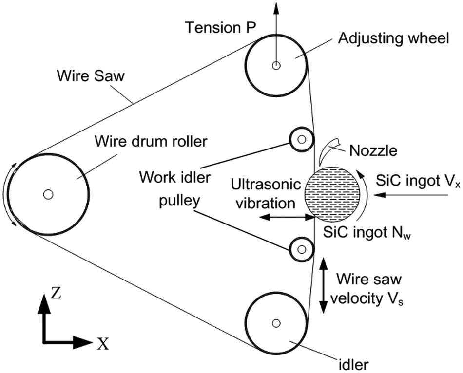
Schematic representation of wire saw machine with ultrasonic vibration.
A Leica DCM 3D dual core 3D measuring microscope from Sensofar-Tech, S.L., is used to measure the part surface roughness, such as the arithmetic mean deviation, maximum height, root mean square height skewness and steepness. To compare the surface roughness of different parts, the root mean square height is used
where A is the area of assessment and Z(x, y) is the profile height at location (x, y). The material machined is a SiC monocrystal with SiC mass fraction of 95%, density of 3.20–3.25 g/cm3 and fiber stiffness of 2840–3320 kg/mm2. The wire is stainless steel with a nickel matrix, plated with the diamond abrasive JR2. The abrasive size is 30–40 µm, the saw wire length is 50 m and the average wire saw diameter is 0.29 mm.
Experimental scheme
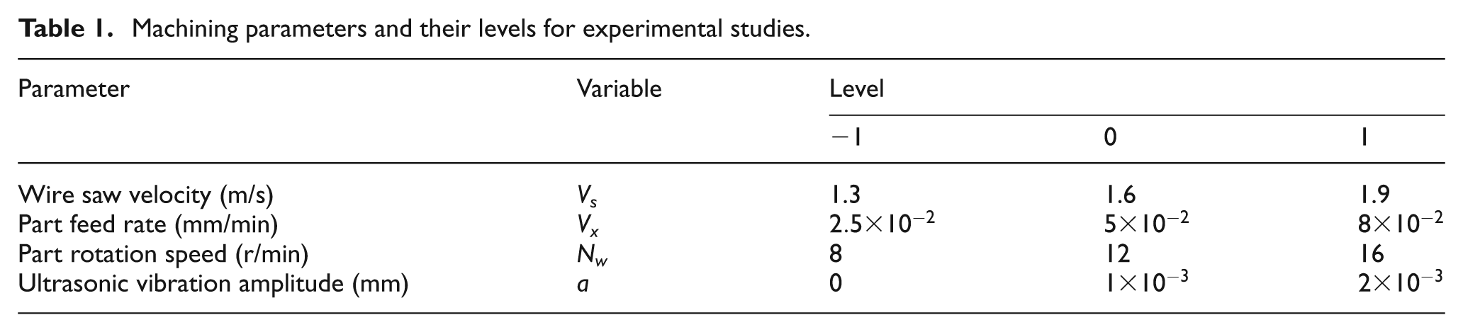
When wire saw cutting SiC monocrystal wafers with ultrasonic vibration, the possible factors that influence surface roughness include wire tension, velocity, wear and vibration, part rotation speed, feed rate, ultrasonic vibration frequency and amplitude, coolant and so on. This study focus on the process parameters that have a major effect on the surface roughness of SiC monocrystal wafers: wire saw velocity (Vs), part feed rate (Vx), part rotation speed (Nw) and ultrasonic vibration amplitude (a). The four factors are independent variables and have ranges of 1.3–1.9 m/s, 2.5–8 × 10⁻² mm/min, 8–16 r/min and 0–2 × 10⁻² mm. If the wire saw velocity is less than 1.3 m/s, the cutting productivity is very low and, if the wire saw velocity is more than 1.9 m/s, roller vibration will occur, leading to machine tool vibrations that damage the wafer and make the machining process unstable. If the feed rate is less than 0.025 mm/min, the machining productivity is very low and instability of the feed system may occur. If the feed rate is more than 0.1 mm/min, the contact length between the part and wire saw will increase, which will increase the cutting force and negatively impact the surface roughness. Part rotation speeds less than 8 r/min will decrease productivity; however, when the part rotation speed is more than 16 r/min, the inertial impact of the cutting force is large, especially when the part’s tangential velocity and the wire saw velocity are in the opposite directions, leading to inferior surface quality and an unstable cutting process. The CCD design factors and levels are given in Table 1. In the experiments conducted in this article, the wire tension is constant (0.2 MPa). While wire tension does have some effect on roughness, the effect is minor as compared to the feed rate, ultrasonic vibration amplitude, wire saw velocity and part rotation speed. This is explored in more detail later in this article.
Machining parameters and their levels for experimental studies.
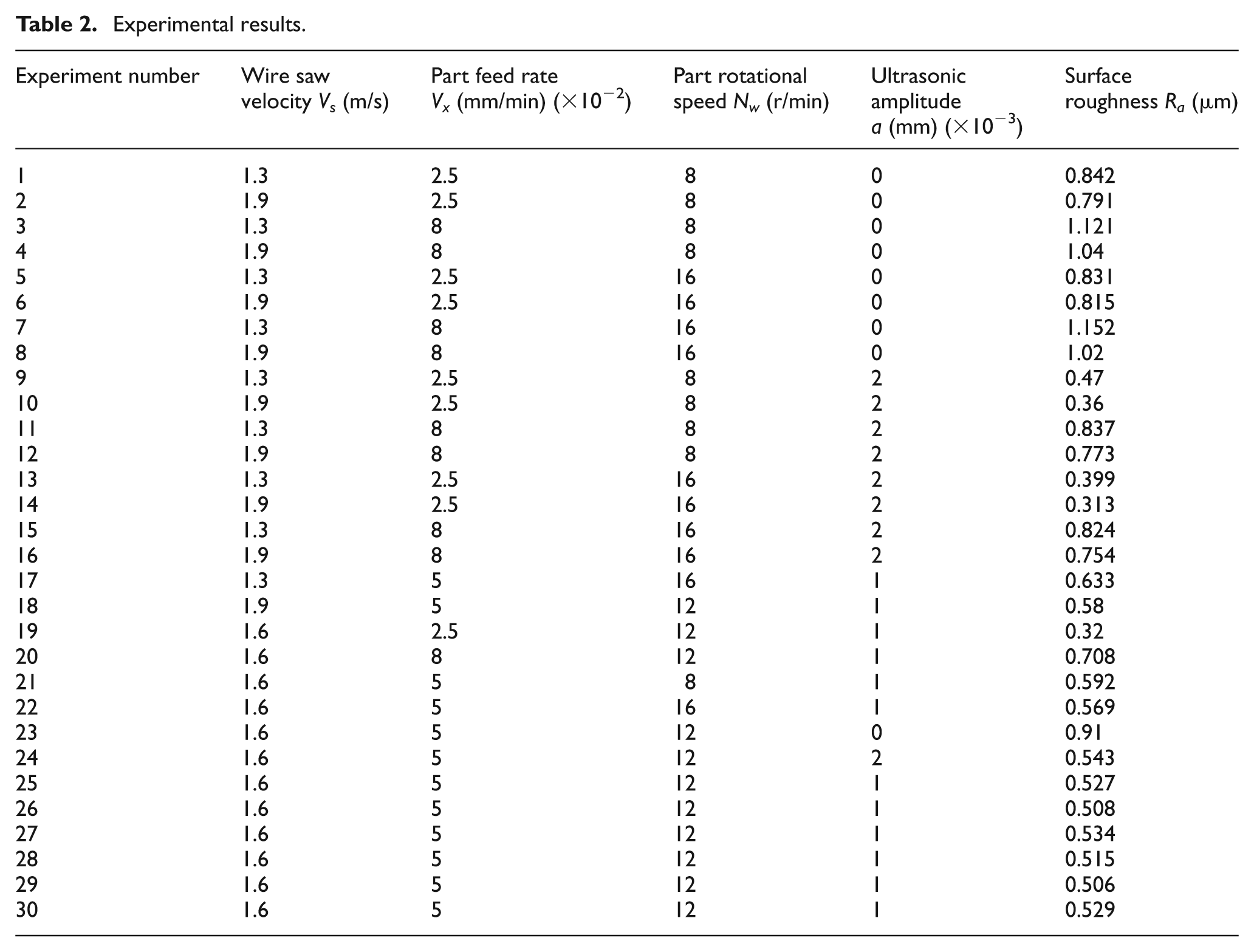
The surface roughness is measured at six points on each wafer, evenly spaced from the center to the edge of the wafer, and average values are used for analysis. A scanning electron microscope (SEM) is used to measure the machined surface. Table 2 shows the experimental data.
Experimental results.
Modeling and optimization of process parameters
The modeling and optimization approach utilized in Palanikumar et al. 28 for machining metal matrix composites will be utilized in this article. The RSM approach is used in this study to determine the relationship between the surface roughness and the process parameters (i.e. wire saw velocity, part feed rate, part rotation speed and ultrasonic vibration amplitude) when wire saw machining SiC monocrystal wafers. The RSM approach establishes a continuous variable surface and evaluates the factors affecting the process parameters and their interactions in order to determine the optimal process parameters. Based on the data from designing and conducting wire saw machining experiments, multiple quadratic regression equations are used to relate the process parameters to the surface roughness. The optimal process parameters for minimizing surface roughness are obtained by analyzing the regression equation.
A general second-order polynomial response surface mathematical model that is often used is
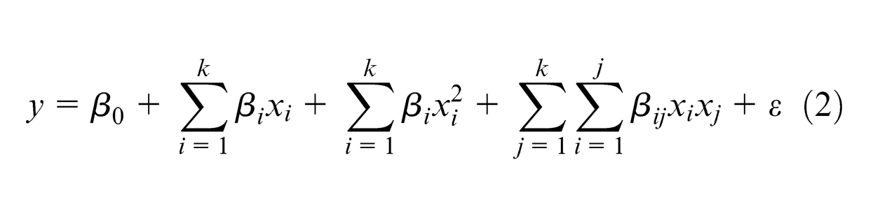
where y is surface roughness, k is the number of process parameters, βs are constants, xi is the value of the ith process parameter and ε is the residual (i.e. experimental error).
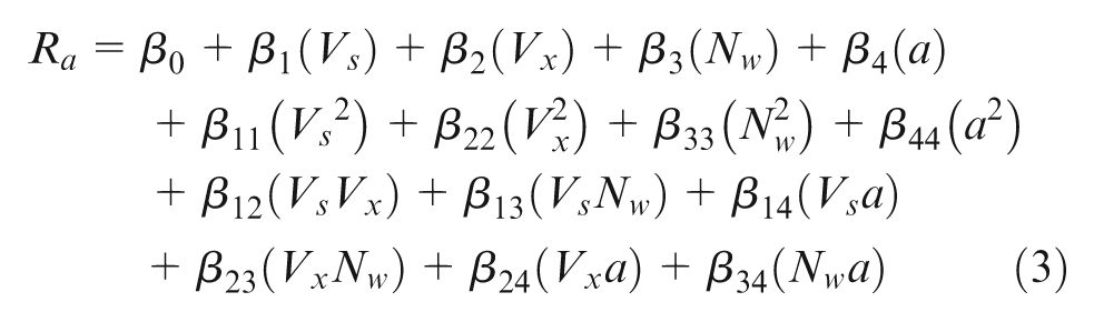
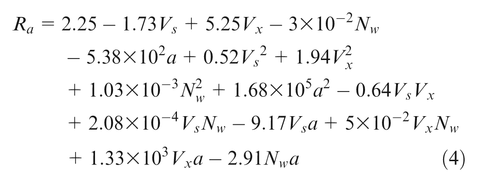
In this study, a mathematical model is built for correlating the interactive and higher-order influences of various process parameters to the surface roughness when wire saw machining SiC monocrystal wafers. The relationship between the surface roughness and process parameters using a second-order response surface is
ANOVA is now used to evaluate the adequacy of the model by separating the total variation in the experiments into parts due to the controlled factors and part due to error. Table 3 shows the resulting model coefficients.
Surface roughness model coefficients.
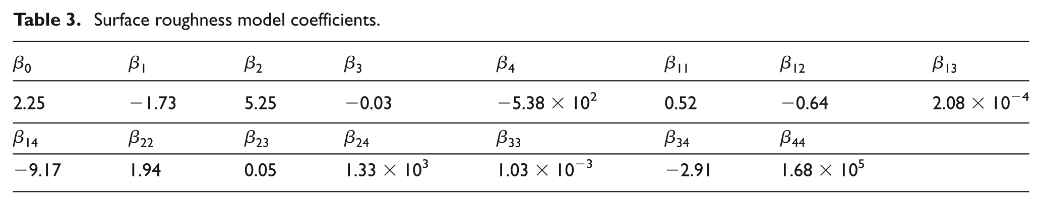
Table 4 shows the results when applying ANOVA. In this table, SS is the sum of squares of the variable, DF is the degrees of freedom of the variables and MS, the mean square, is the SS divided by the DF. The parameter F refers to the F value, which is an index that is used to check the model adequacy. If the F value is greater than the value given in the F-table, the model is accurate with a 95% confidence level. The F value is the ratio between the variance of the process parameters or interactive items (between two process parameters) and the residual variance. The greater the F value, as compared to the table F value, the more significant the independent variable’s influence on the surface roughness. In statistical significance testing, the p value is the probability of obtaining a test statistic at least as extreme as the one that was actually observed, assuming that the null hypothesis is true. In this context, the value a is considered more “extreme” than the value b if a is less likely to occur under the null hypothesis. One often “rejects the null hypothesis” when the p value is less than the significance level α, which is often 0.05 or 0.01.
ANOVA results for response surface model.
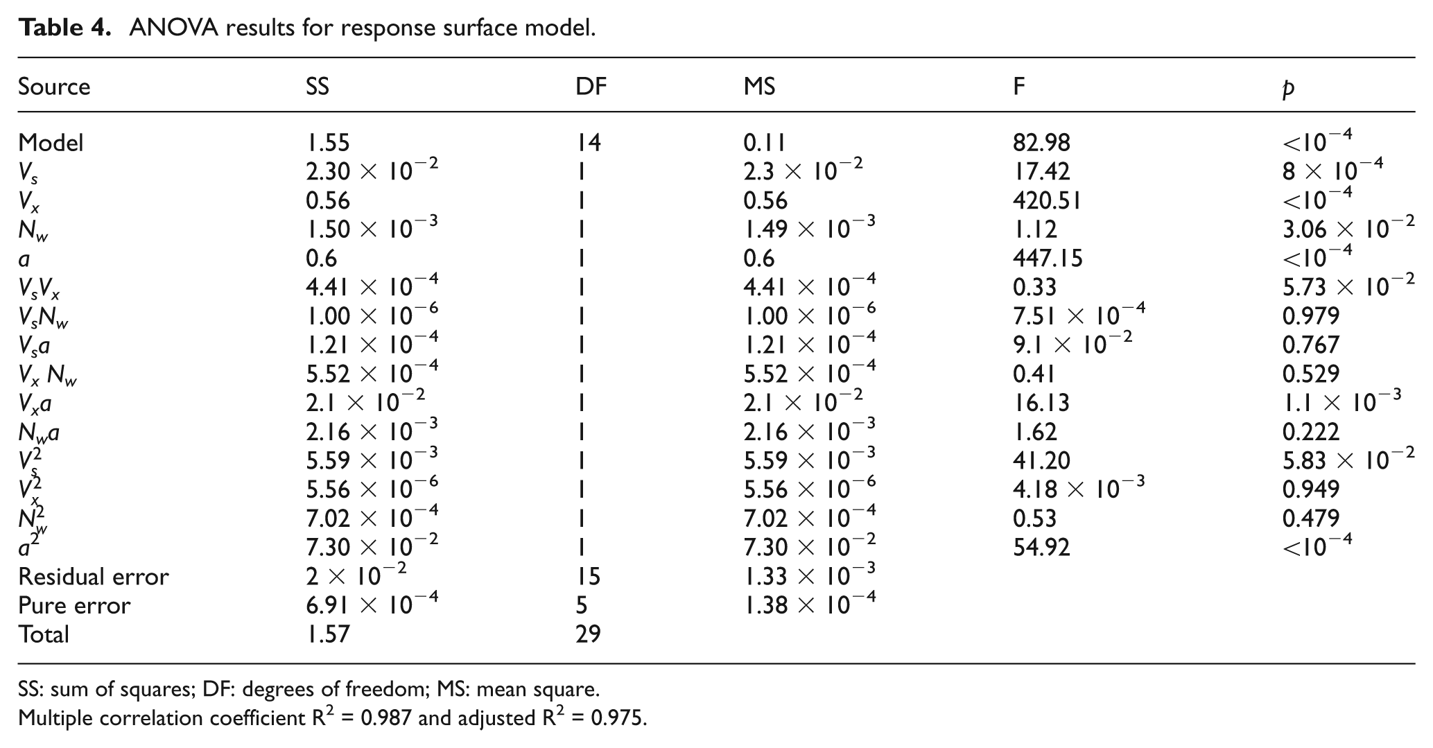
SS: sum of squares; DF: degrees of freedom; MS: mean square
Multiple correlation coefficient R2 = 0.987 and adjusted R2 = 0.975.
The mathematical model correlating surface roughness and process parameters when wire saw machining SiC monocrystal wafers is
Based on the ANOVA for the quadratic surface roughness model in Table 4, it can be seen that FM = 82.98 > F0.01(14, 15) = 3.56 and p < 10−4, indicating the model is highly significant (i.e. the model can express the relationship between surface roughness and process parameters well). From the values of p in Table 4, it can be seen that Vs, Vx, a and Vxa reached highly significant levels (p < 10−2). Therefore, wire saw velocity, part feed rate, ultrasonic vibration amplitude and the interaction between part feed rate and ultrasonic vibration amplitude significantly impact the surface roughness when wire saw machining SiC monocrystal wafers. Based on the F values for each factor, the order of significance (i.e. degree of the factors influencing surface roughness) is (1) ultrasonic vibration amplitude, (2) part feed rate, (3) wire saw velocity and (4) part rotational speed.
The model accuracy is further analyzed using multiple correlation coefficient R2 values. In this study, R2 = 0.9873, showing that there is 97.54% change in the response value (surface roughness) from the process parameters (wire saw velocity, part speed, part feed rate and ultrasonic vibration amplitude), and that a high correlation exists between the experimental and predicted surface roughness values.
The experimental data and the data predicted using the model are plotted against one another in Figure 2, illustrating a good correlation between the model and experimental values. Therefore, the model can be used to predict the surface roughness well when wire saw machining SiC monocrystal wafers within the range of 15.6% difference. The ANOVA from the regression analysis shows that the one-degree terms’ ultrasonic vibration amplitude a and part feed rate Vx and the quadratic terms’ ultrasonic vibration amplitude a2 and wire saw velocity
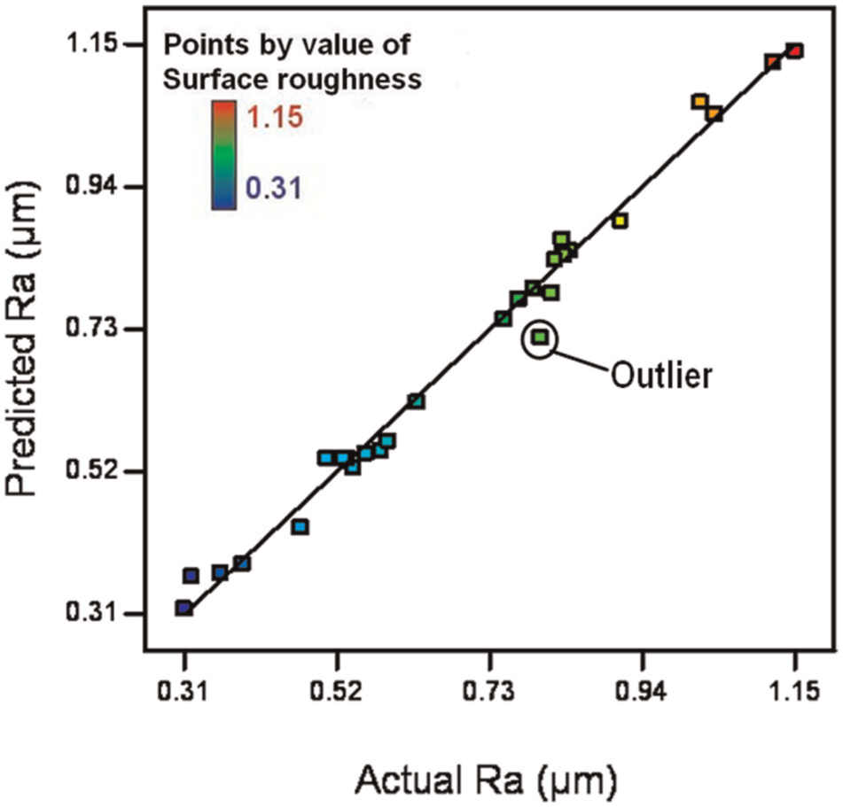
Relationship between predicted and actual surface roughness.
To improve the surface quality of SiC monocrystal wafers, the wire saw machining process parameters should be optimized. In this study, response optimization analysis is conducted, using the developed mathematical model, for attaining the minimum surface roughness when wire saw machining SiC monocrystal wafers. The desirability function–based approach is now used to determine the optimal process parameters. In this approach, the measured properties of each predicted response are transformed into a dimensionless desirability value d, which is between 0 and 1. 29 A value of d = 0 means the response is completely unacceptable and a value of d = 1 means the response is the optimized value (i.e. the surface roughness is 0.26 µm). A one-sided transformation is used to transform the response into a desirability
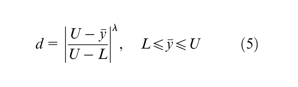
where λ is a weight and
Providing the desirability for the surface roughness;
Maximizing the desirability and analyzing the optimal value.
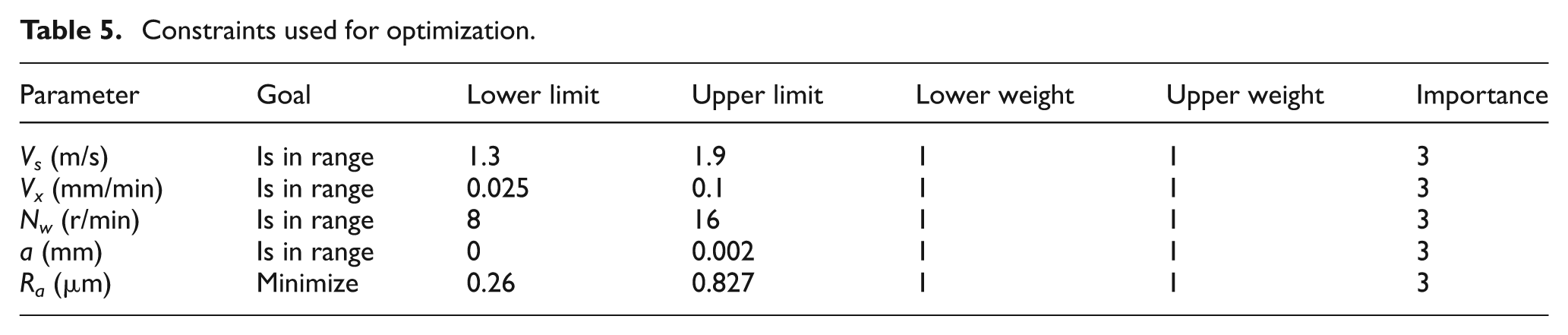
The process parameters, their limits and the objective function optimization goal settings are given in Table 5.
Constraints used for optimization.
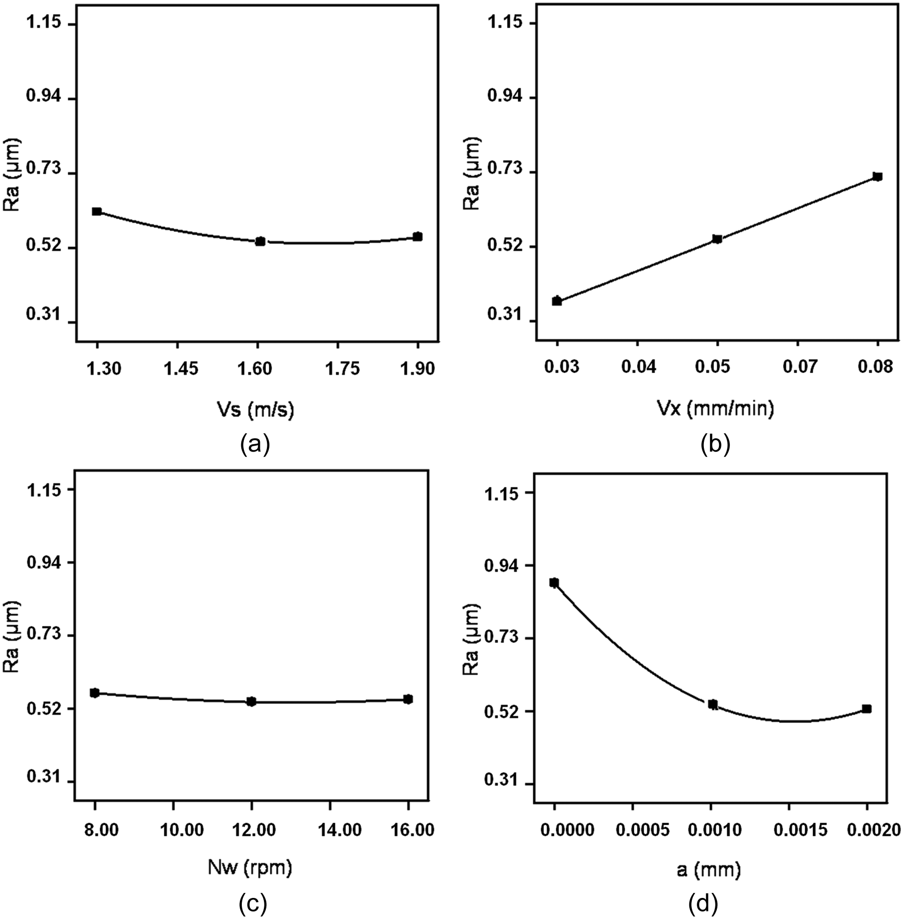
In the desirability-based approach, different solutions are obtained and the solution with the highest desirability is preferred. In this study, the optimal solution corresponds to the maximum desirability value of 0.978. The contour desirability values are presented in Figure 3. Since the process parameters with the greatest satisfaction are optimal, the optimal process parameters are Vs = 1.71 m/s, Vx = 2.5 × 10⁻³ mm/min, Nw = 14.76 r/min and a = 1.67 × 10⁻³ mm. The optimization solutions for each machining parameter are shown in Figure 4, where Figure 4(a) represents the relationship between Vs and Ra for Vx = 5 × 10⁻² mm/min, Nw = 12 r/min and a = 10−3 mm; Figure 4(b) represents the relationship between Vx and Ra for Vs = 1.6 m/s, Nw = 12 r/min and a = 10−3 mm; Figure 4(c) represents the relationship between Nw and Ra for Vs = 1.6 m/s, Vx = 5 × 10⁻² mm/min and a = 10−3 mm and Figure 4(d) is the relationship between a and Ra for Vs = 1.6 m/s, Vx = 5 × 10⁻² mm/min and Nw = 12 r/min. The optimal process parameters are Vs = 1.71 m/s, Vx = 2.5 × 10⁻² mm/min, Nw = 14.76 r/min and a = 1.67 × 10⁻³ mm. The resulting optimal surface roughness is 0.26 µm.
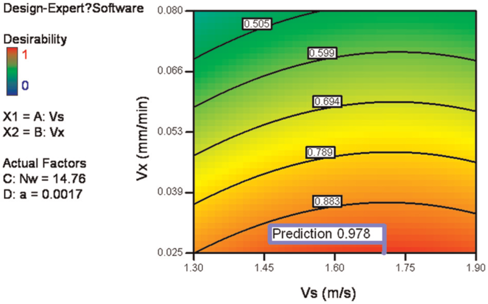
Contour graphs at maximum desirability value of 0.978 (Nw = 14.76 r/min and a = 1.67 × 10⁻³ mm).
Optimal solutions for surface roughness.
Results and discussion
RSM of surface roughness of SiC monocrystal wafers
The surface roughness of SiC monocrystal wafers greatly impacts post-processing operations, such as lapping and polishing, and the function of the IC devices in which they are used. In this study, RSM is used for predicting the surface roughness when wire saw machining SiC monocrystal wafers. Figure 5 is a plot of the normal probability of the residuals, which is used to determine whether the residuals follow a normal distribution. The straight line in Figure 5 is the expectations of the residuals. Since the residues are very close to the expectations, the distribution is considered normal. Figure 6 is a plot of the residuals versus the experimental sequence. The straight line in the middle of Figure 6 means the residual is 0. The top straight line indicates the upper limit of the residual range and the bottom straight line indicates the lower limit of the residual range. It can be seen that the residuals distribute uniformly around 0, and no missing or isolated point exists. Therefore, the developed model can explain the relationship between the surface roughness and the process parameters very well. 30 The residual is calculated against the order of experimentation and is used to estimate the correlation between the residuals. The residual plot in Figure 6 shows that the residuals are distributed evenly in both the positive and negative directions. No evidence of missing terms exists and, hence, the model can be used to predict the surface roughness in the SiC wire saw machining process.
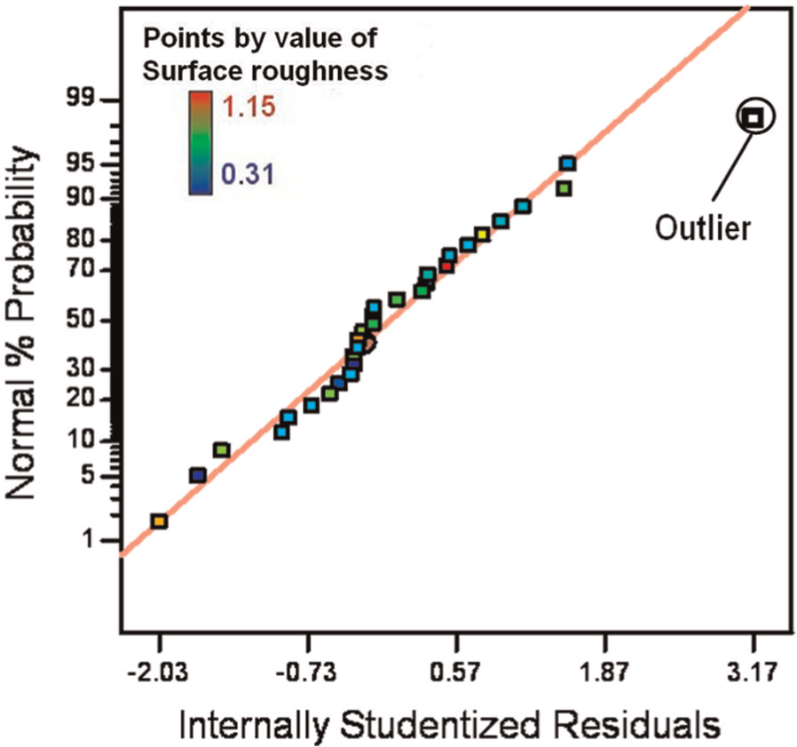
Normal probability of residuals.
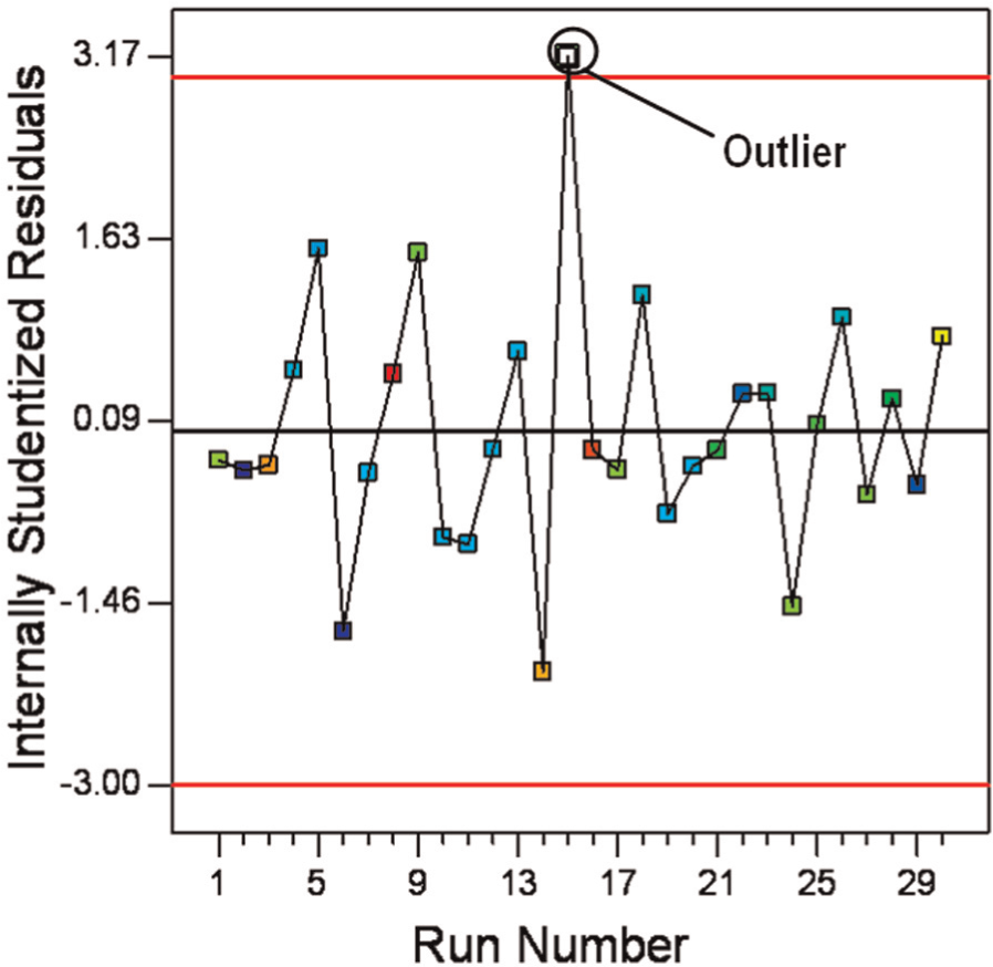
Residual graph.
Response surface analysis for surface roughness of SiC monocrystal wafers
The influence of the process parameters on surface roughness when machining SiC monocrystal wafers is evaluated using RSM. Figures show the various 3D surface plots of surface roughness versus two of the process parameters. The surface plots are drawn using the RSM model and varying two different process parameters while keeping the other two process parameters at their middle levels.
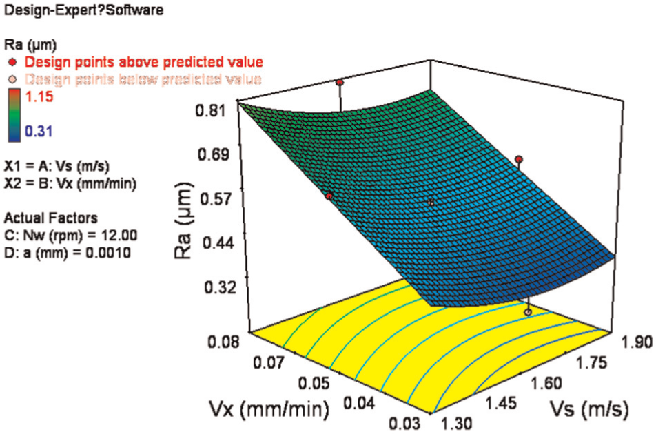
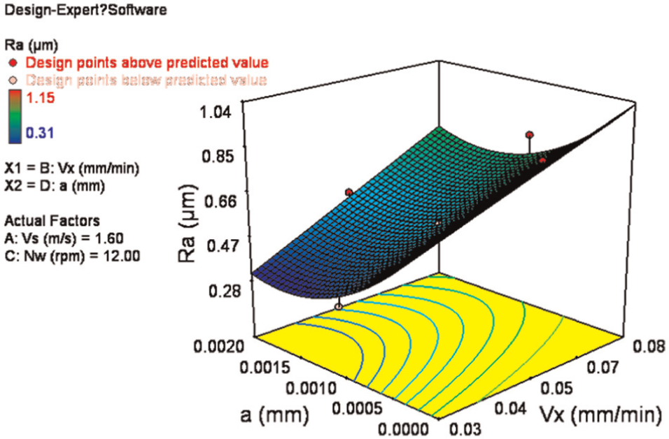
Figure 7 shows the relationship between surface roughness and wire saw velocity and part feed rate. This figure indicates that an increase in part feed rate increases the surface roughness and vice versa. As the part feed rate is increased, the depth of cut for a single abrasive in the wire saw is increased, which leads to an increase in the friction force between the wire saw and wafer, thus, increasing surface roughness. Another reason is the contact length, illustrated in Figure 8, between the wire saw and part increases when the part feed rate increases; thus, the force between the wire saw and part increases, making the surface roughness of SiC monocrystal wafer worse.
Three-dimensional surface plot of Ra = f(Vs, Vx) for Nw = 12 r/min and a = 10−3 mm.
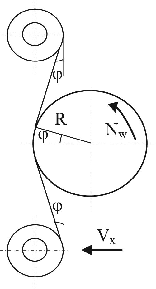
Schematic illustration of contact length between wire and part in wire saw cutting process where R is part radius (mm) and ϕ is half the contact angle between wire and part (rad).
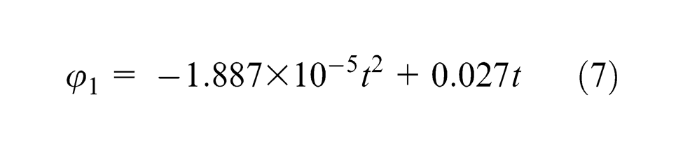
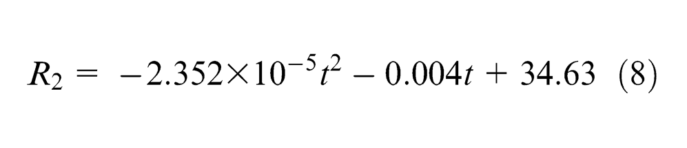
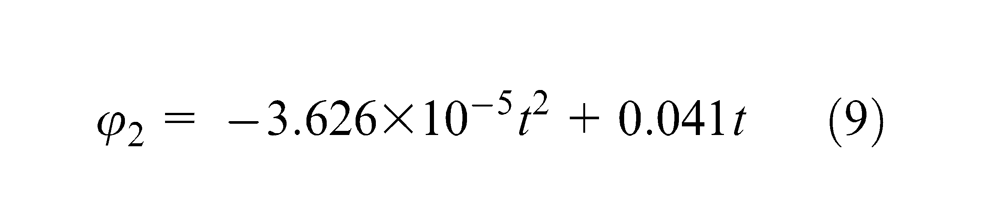
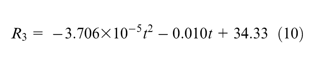
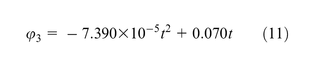
An experiment is conducted using a wire with a length of 50 m and reciprocating motion. Part feed rates of 0.025, 0.05 and 0.08 mm/min are selected and the part radius contact angle between the wire saw and part is measured every 20 min. Using the measurements and applying least squares, the change in part radius and contact angle are modeled as given in the following and are shown in Figures 9 and 10, respectively. The radius and contact half angle, respectively, when Vx1 = 0.025 mm/min, are
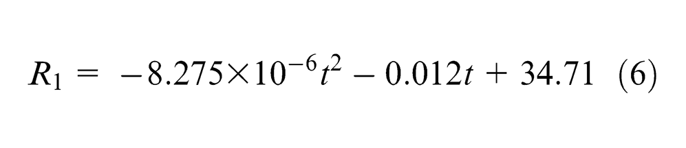
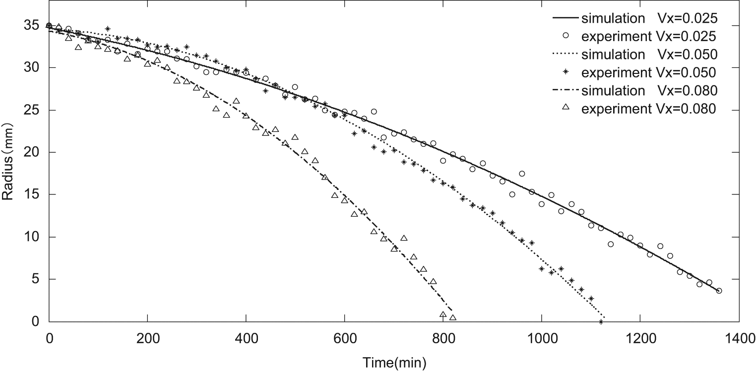
Part radius during wire saw cutting process for various feeds. Points are experimental data.
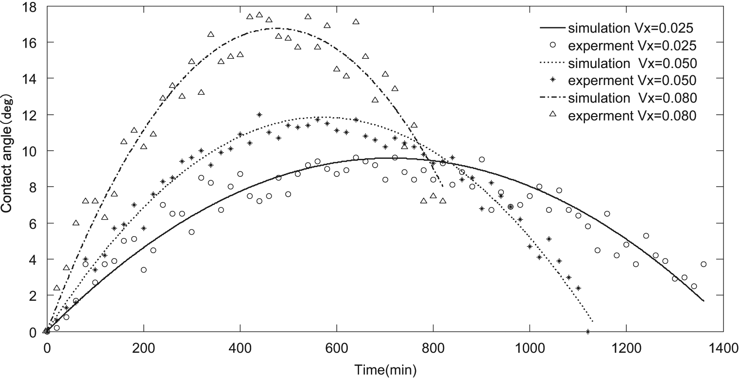
Contact angle during wire saw cutting process for various feeds. Points are experimental data.
The radius and contact half angle, respectively, when Vx2 = 0.05 mm/min, are
The radius and contact half angle, respectively, when Vx3 = 0.08 mm/min, are
The contact length between wire saw and part is
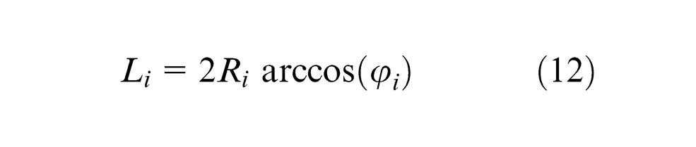
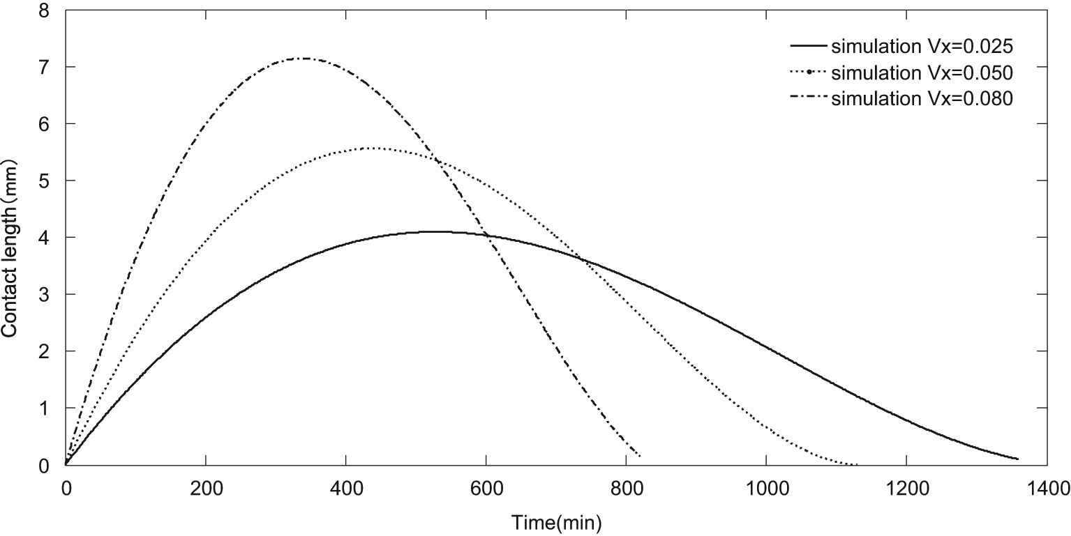
where Ri is the part radius at measurement i (mm) and ϕi is half the contact angle between the wire and part at measurement i (rad). The experimental and simulated contact length between the wire saw and part is shown in Figure 11.
Contact length during wire saw cutting process for various feeds.
From Figure 11, it can be seen that as the feed rate increases, the rate of change of the contact length increases and the maximum contact length increases; therefore, the maximum cutting force will increase with increasing feed rate, leading to worse surface roughness. Figure 12 visually shows how the contact length varies as the process progresses. This was illustrated by performing glass cutting, which also allowed the contact angle and part radii to be easily measured.
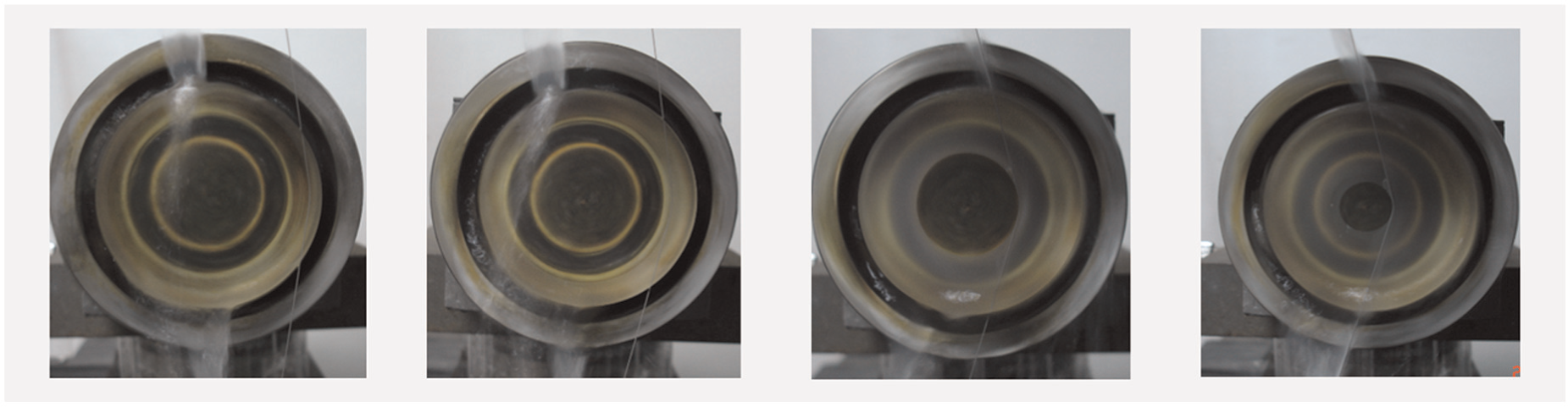
Contact length for various part radii.
Figure 7 indicates that surface roughness decreases as wire saw velocity increases from 1.3 to 1.7 m/s. As the wire saw velocity increases, the number of abrasives on the wire saw per unit length that cut the part is increasing; therefore, the depth of cut of each abrasive decreases, which decreases the surface roughness. However, as wire saw velocity increases from 1.7 to 1.9 m/s, the surface roughness increases. A possible reason for this affect is that in this range of wire saw velocity, the work idler pulleys and the machine tool vibration increase.
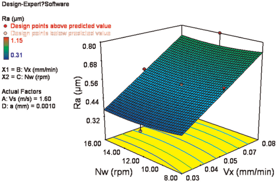
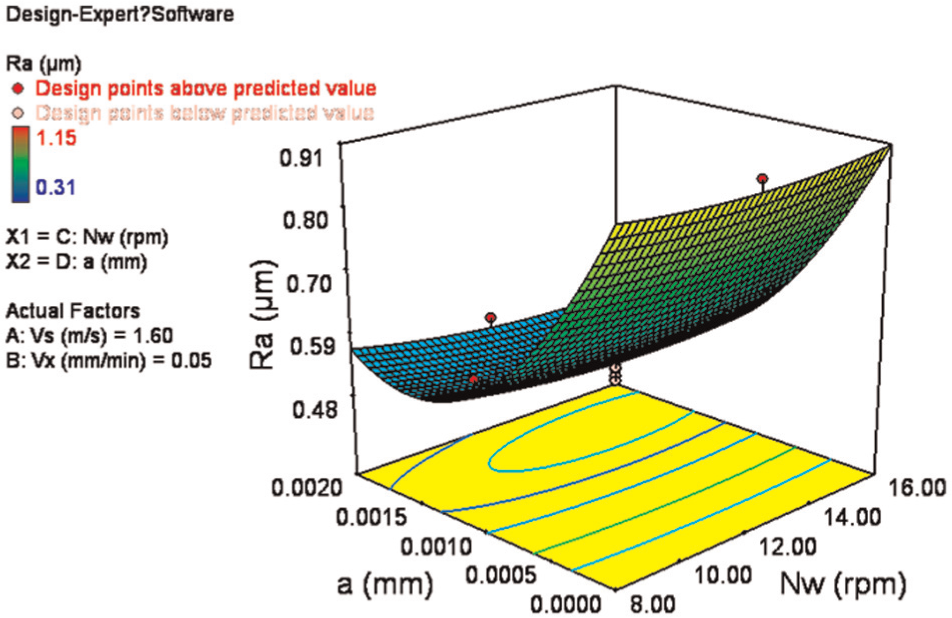
Figure 13 shows the influence of wire saw velocity and part rotational speed on surface roughness. This figure shows that the part rotation speed’s influence on surface roughness is quite small, as the surface roughness only varies from 0.5123 to 0.5648 µm. In this study, the aim of the part rotation is to try to make the contact, and thus, the friction, between the wire saw and part constant, and increase productivity as the wire saw is only required to cut half of the part diameter.
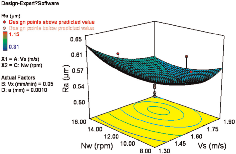
Three-dimensional surface plot of Ra = f(Vs, Nw) for Vx = 5 × 10⁻² mm/min and a = 10−3 mm.
Figure 14 shows the influence of wire saw velocity and ultrasonic vibration amplitude on surface roughness. This figure shows that the increase in ultrasonic vibration amplitude produces a very appreciable change in surface roughness (from 0.4632 to 0.8889 µm) when wire saw machining SiC monocrystal wafers. The reason for the decrease in surface roughness is that ultrasonic vibration transforms continuous contact between the wire saw and part into periodic contact. Therefore, the cutting force due to the rubbing and plowing part of the friction force will be greatly diminished, and the number of wire saw and part impacts will be decreased, leading to less wire damage and prolonged wire life. The periodic contact decreases the cutting area temperature and allows the coolant to more easily enter the cutting area, which further decreases the cutting area temperature. The decrease in temperature changes the friction coefficient between the wire saw and part and leads to improved surface roughness when processing SiC monocrystal wafers. The schematic diagram for the wire saw cutting process with and without ultrasonic vibration is shown in Figure 15.
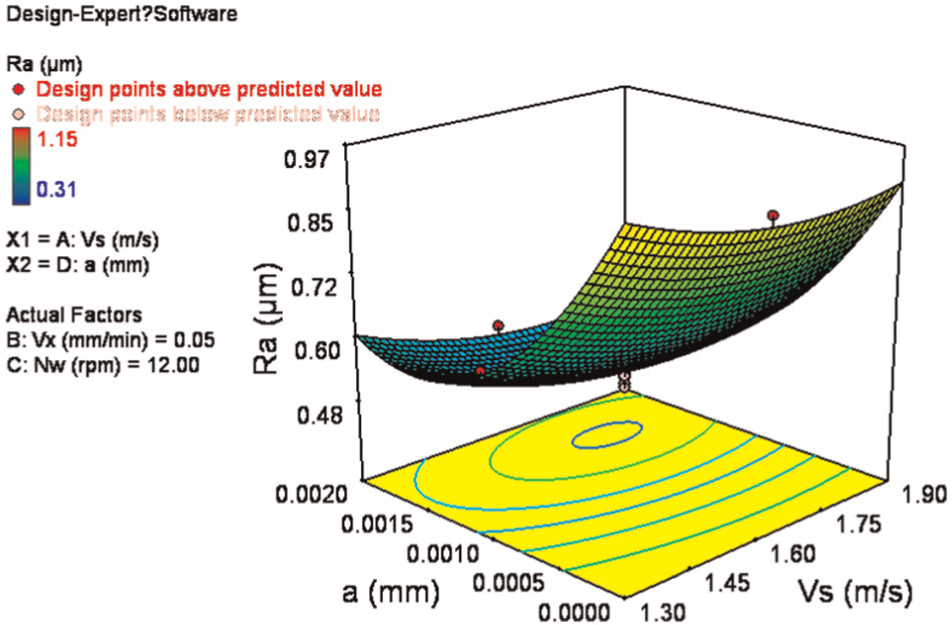
Three-dimensional surface plot of Ra = f(Vs, a) for Nw = 12 r/min and Vx = 5 × 10⁻² mm/min.
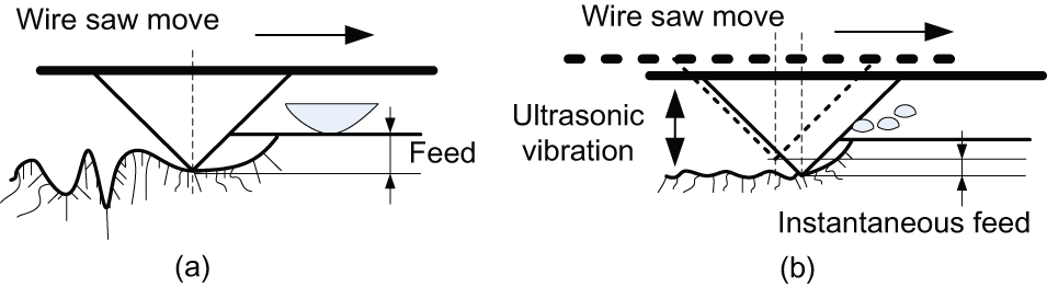
Schematic diagram for wire saw cutting process without and with ultrasonic vibration.
The SEM images when wire saw machining without and with ultrasonic vibration for the same number of wafers are shown in Figure 16. Figure 16(a) and (b) shows the wire saw wear after cutting one wafer of diameter 102 mm without and with ultrasonic vibration, respectively. The wire saw has severe wear (Figure 16(a)) and slight wear (Figure 16(b)), illustrating that the friction and temperature are decreased when using ultrasonic vibration.
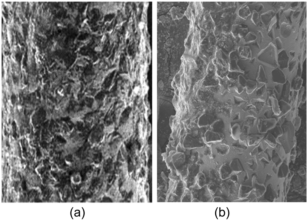
Wire saw wear (a) without and (b) with ultrasonic vibration (Vs = 1.9 m/s, Vx = 2.5 × 10⁻² mm/min, Nw = 16 r/min and a = 1.8 × 10⁻³ mm).
Ultrasonic vibration makes the critical depth of cut larger. Studies have shown that the mechanism for brittle material processing is similar to the mechanism for ductile material processing when ultrasonic vibration is utilized.21,31,32 This is also true for the turning process where the critical of depth of cut with the aid of ultrasonic vibration was larger than without the aid of ultrasonic vibration. 33 Third, the possible reason could be high-pressure phase transformation. The research in Patten et al. 13 shows that SiC experiences a ductile-to-brittle transition similar to other nominally brittle materials such as silicon, germanium and silicon nitride. It is believed that the ductility of SiC during machining is due to the formation of a high-pressure phase at the cutting edge, which encompasses the chip formation zone and its associated material volume. This high-pressure phase transformation mechanism is similar to that found with other semiconductors and ceramics, leading to a plastic response rather than brittle fracture at small size scales. All the above reasons show that the ultrasonic vibration has a significant effect on the wafer surface roughness.
The surface profile observed in machining a SiC monocrystal wafer with process parameters Vs = 1.9 m/s, Vx = 2.5 × 10⁻² mm/min and Nw = 16 r/min is presented in Figure 17(a), and the surface profile using same process parameters with ultrasonic amplitude a = 1.8 × 10⁻³ mm is presented in Figure 17(b). The optical microscope images reveal that the two different machining methods have quite different topographies. There are large peaks and valleys in Figure 17(a) made by the wire being in contact with the part constantly, while in Figure 17(b) there are only very small peaks and valleys. Furthermore, an SEM image of a machined surface when wire saw machining SiC monocrystal wafers without and with ultrasonic vibration is presented in Figure 18(a) and (b), which also illustrates that ultrasonic vibration has a significant effect on the wafer surface quality.
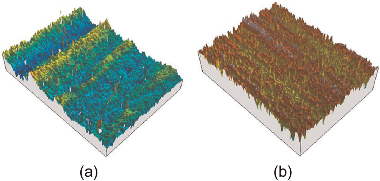
Microscope pictures of wafer surface (a) without (Ra = 0.815 µm) and (b) with ultrasonic vibration (Ra = 0.313 µm) (Vs = 1.9 m/s, Vx = 2.5 × 10⁻² mm/min, Nw = 16 r/min and a = 1.8 × 10⁻³ mm).
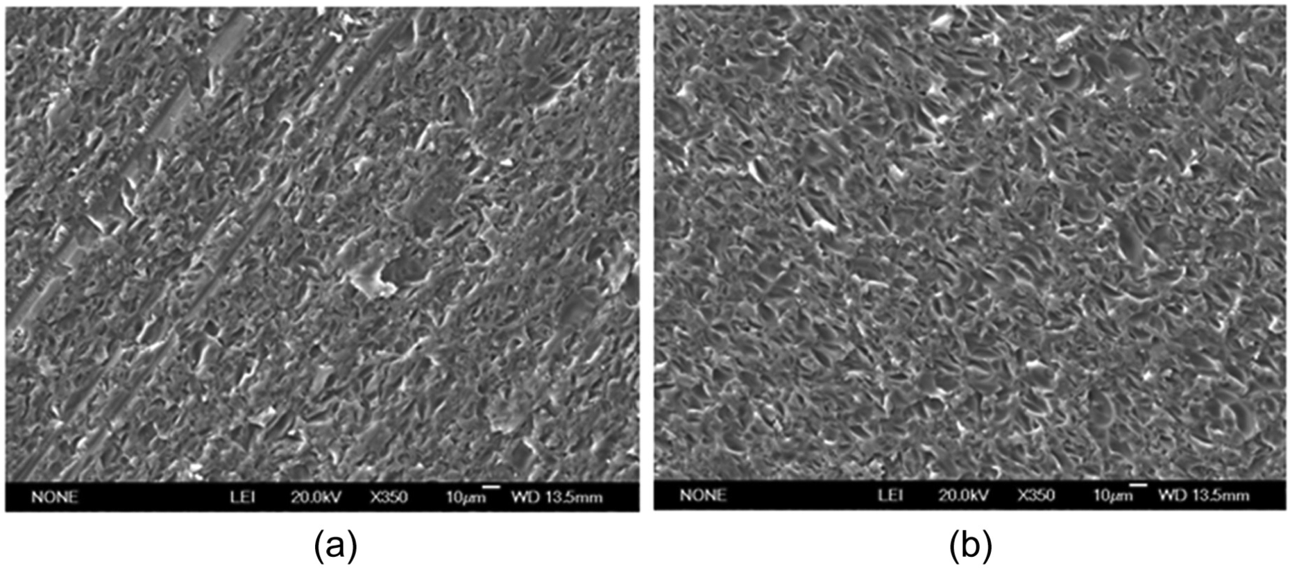
SEM pictures of SiC wafers (a) without and (b) with ultrasonic vibration (Vs = 1.9 m/s, Vx = 2.5 × 10⁻² mm/min, Nw = 16 r/min and a = 1.8 × 10⁻³ mm).
Figures 8 and 9 also indicate that surface roughness decreases as wire saw velocity increases when wire saw velocity is low and increases as wire saw velocity increases when the wire saw velocity is high. The simulation data are consistent with the experimental results. With the part feed rate and rotation speed fixed, the abrasive depth of cut decreases when the wire saw velocity increases (from 1.3 to 1.7 m/s); thus, the wafer’s surface roughness decreases. When the wire saw velocity increases to some extent from 1.7 to 1.9 m/s, the increasing roller rotation speed leads to machine tool vibrations that make the wafer’s surface roughness worse.
Figure 19 shows the surface plot of surface roughness with respect to part rotation speed and part feed rate. This figure shows that an increase in part feed rate, which leads to an increase in the abrasive depth of cut, causes an increase in the wafer’s surface roughness and vice versa. Figure 19 indicates that the part rotation speed has very little impact on the surface roughness, as compared to part feed rate. Figure 20 shows the surface plot of surface roughness with respect to part feed rate and ultrasonic vibration amplitude. This figure indicates that both part feed rate and ultrasonic vibration amplitude have a significant impact on surface roughness. Figure 20 indicates that the surface roughness decreases significantly as the ultrasonic vibration amplitude increases from 0 × 10−3 to 1.6 × 10⁻³ mm and decreases less significantly as the ultrasonic vibration amplitude increases from 1.6 × 10⁻³ to 2 × 10⁻³ mm. Figure 21 shows the influence of part rotation speed and ultrasonic vibration amplitude on surface roughness. This figure shows that the increase in ultrasonic vibration amplitude within the range of 0 to 10−3 mm has a very appreciable change in surface roughness when wire saw machining SiC monocrystal wafers. Figures 19 and 21 also indicate that the part rotation speed has little impact on surface roughness.
Three-dimensional surface of Ra = f(Nw, Vx) for Vs = 1.6 m/s and a = 10−3 mm.
Three-dimensional surface of Ra = f(a, Vx) for Vs = 1.6 m/s and Nw = 12 r/min.
Three-dimensional surface of Ra = f(Nw, a) for Vs = 1.6 m/s and Vx = 5 × 10⁻² mm/min.
The effect of wire tension on wafer surface roughness is also investigated. The wire tension is 0.18, 0.20, 0.21 and 0.22 MPa, respectively, and the other parameters are Vs = 1.9 m/s, Vx = 2.5 × 10⁻² mm/min, Nw = 16 r/min and a = 1.0 × 10⁻³ mm. Eight points for each wafer are measured from the center to the edge of wafer at the same interval, and the mean surface roughness is shown in Figure 22. It can be found that the surface roughness decreases as the wire tension increases, and the difference in the surface roughness is not significant as wire tension varies. The mean surface roughness for each wire tension is 0.507, 0.525, 0.569 and 0.602 µm.
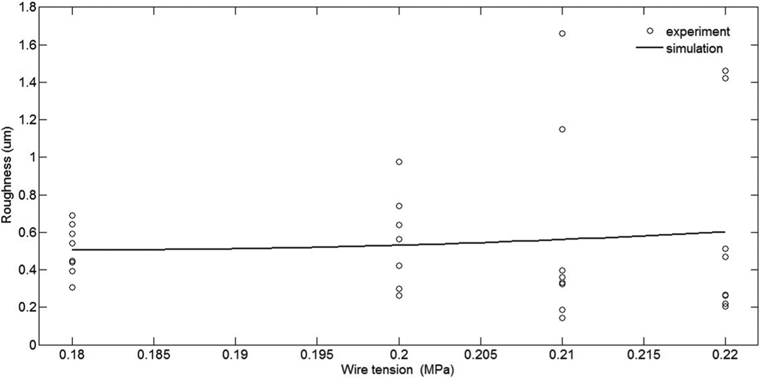
Surface roughness for different wire tensions.
Model validation
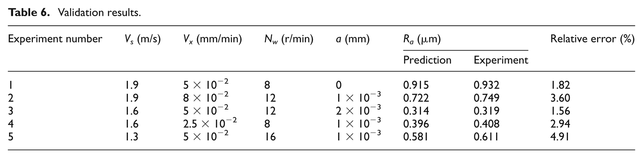
The developed model and resulting optimal cutting conditions are validated by conducting further experiments. The five sets of machining parameters provided in Table 6 are used for validation experiments. From the analysis of the data in Table 6, it can be seen that the developed RSM model has a close correlation with the experimental results as the relative errors are less than 5%. Also, the cutting conditions in experiment 3, which is closest to the optimal cutting conditions, produce the best surface roughness.
Validation results.
Summary and conclusion
Experiments were conducted for wire saw machining of SiC monocrystal wafers using the CCD experimental scheme. The process parameters considered for the present study are wire saw velocity, part feed rate, part speed and ultrasonic vibration amplitude. Using RSM, an empirical relationship is developed for the surface roughness and, based on this relationship, the cutting conditions when wire saw machining with ultrasonic vibration SiC monocrystal wafers are optimized with the desirability function–based approach. The following conclusions can be drawn from this study:
The model adequacy was examined and was found to be adequate at a 95% confidence level. Therefore, the model can be used for predicting the surface roughness when wire saw machining SiC monocrystal wafers within the range of process parameters considered in this study.
The results indicate that an increase in ultrasonic vibration amplitude within the range from 0 to 1.67 × 10⁻³ mm produces a very appreciable decrease in surface roughness and increasing the wire saw velocity reduces the surface roughness, whereas the increase of part feed rate increases the surface roughness and the part rotation speed has little impact on surface roughness. The optimal process parameters are Vs = 1.71 m/s, Vx = 2.5 × 10⁻² mm/min, Nw = 14.76 r/min and a = 1.67 × 10⁻³ mm. With these process parameters, the optimal surface roughness of SiC monocrystal wafers is 0.26 µm.
The developed model in this article and resulting optimal conditions were validated by conducting further experiments. Validation experiments were conducted for five sets of machining parameters, and the relative error between the prediction and experiment was less than 5%.
Footnotes
Declaration of conflicting interests
The authors declare that there is no conflict of interest.
Funding
This study was supported by the National Natural Science Foundation of China (51175420) and the Shaanxi Province Education Department (11JK0849/11JS074).