
Abstract
Photovoltaic industry requires the cutting of silicon ingots into wafers in order to get minimum kerf loss, to facilitate manufacturing of thin wafers and to provide high productivity. Existing silicon ingot slicing processes like inner diameter saw and abrasive wire cutting have drawbacks of high kerf loss, lower finish and limitation on the thickness of wafer. In order to have economically viable photovoltaic technology, efficiency of wafer manufacturing process needs to be improved. The wire–electrical discharge machining technology is adopted as a new candidate for silicon slicing and is compared with the existing procedures and testified whether it can inevitably substitute the inner diameter saw or even compete with wire saws in some manufacturing orders. The main focus of this article is to understand the effect of processing parameters on the cutting process, so the parametric conditions delivering high slicing rate and low kerf loss can be achieved. Modeling of wire–electrical discharge machining is difficult as it involves several disciplines such as thermodynamics, hydrodynamics, electrodynamics and electromagnetics. Various researchers have proposed analytical models for electrical discharge machining and wire–electrical discharge machining through the use of electrothermal concepts. However, a comprehensive model that predicts the erosion rate in wire–electrical discharge machining process is needed. This article considers moving the line heat source nature of the wire to predict the temperature profiles of the workpiece in order to calculate the erosion rate. The results thus obtained have been analyzed experimentally, and conclusions have been derived enabling a better understanding of future research prospects and applications.
Keywords
Introduction
In view of the huge demand of silicon wafers in photovoltaic (PV) applications, requirements of slicing technology of silicon ingots are twofold, that is, maximization of productivity and minimization of manufacturing cost. The PV industry requires cutting of silicon ingots into thin wafers such that the kerf loss is minimum with crack- and damage-free surface.
Conventionally, inner diameter (ID) saws and wire saws have been used for silicon ingot slicing in silicon wafer manufacturing. As these methods are based on mechanical abrasive cutting, the contact forces adversely affect the newly generated surface. The damage may involve generation of surface microcracks or other machining-related damage to the wafer surface. The conventional methods cause high kerf loss, which is in the range of 35%–40%. The minimum wafer thickness that can be attained is in the range of 250–350 µm. The higher kerf loss and wafer thickness with the conventional methods needed the development of alternative methods of silicon ingot slicing.1–5
Wire–electrical discharge machining (EDM) process was first implemented for silicon ingot slicing by Luo et al. 6 They used nickel plating and polarity reversal measures to improve electrical conductivity of silicon. They found that the cutting rate in kerosene is greater than that in emulsion for the identical average current. Uno et al. 7 developed a new slicing method for silicon ingots in which contamination due to adhesion and diffusion of wire electrode material to machine surface could be reduced by using reverse polarity in wire-EDM process. The metal removal rate was found to increase with increasing current. Reynaerts et al. 8 showed that the crystallographic orientations do not have any effect on EDM of silicon. Also, the process facilitates micro-EDM of complex shapes on silicon, which otherwise was proven to be “difficult to machine” by any other methods. Heeren et al. 9 used die sinking type of micro-EDM to generate different shapes. Kunieda and Ojima 10 suggested that plating of P-type silicon by aluminum and N-type silicon by gold antimony improves machining rate dramatically by changing the rectifying contact into ohmic one. As plating of silicon surface with conductive material will reduce Schottky barrier thickness, the applied voltage can easily pass through the barrier with tunneling effect. Takino et al., 11 in their experiments on polished silicon wafers, showed that the wafer surfaces cut in water are rougher than those cut in oil. Takino et al. 12 showed that rough edges on silicon plates while cutting in water and/or oil can be reduced by applying electroconductive vinyl chloride resin masks on silicon plates. Peng and Liao 4 used medium- or heavy-doped silicon ingots for slicing, using wire-EDM process. They found that the temperature rise after a period of discharge reduces the resistivity. Hence, abnormal discharges and the slicing efficiency are more in the submerged cutting condition than in the flushing-type wire-EDM process. Wang et al. 13 used wire electrolytic spark slicing strategy in a hybrid oil/aqueous electrolyte environment, thereby combining electric discharge and anodic etching into a single process. Yu et al. 14 conducted experiments on P-type polycrystalline material and found that the auxiliary power effectively breaks insulation between electrode and workpiece. The auxiliary power will also enhance slicing speed and reduce the kerf width.
It is understood from the above-mentioned literature review that much of the research work on wire-EDM of silicon ingot has been focused on understanding the cutting mechanism by wire-EDM via primarily focusing on certain representative cuts that are taken on the silicon work material. The length of the cut taken in most of the researches is very limited to represent the real-life wafer cutting process truly. Therefore, this work presents a cutting over entire length of wafer using wire-EDM and analysis for effects of processing parameters on voltage–current (V-I) characteristics and productivity parameters such as slicing speed and kerf loss besides the mechanism of cutting and quality of surface generated. A comprehensive experimentation has been undertaken to illustrate the above-mentioned aspects. The following sections give details of this investigation.
Experimental setup and procedure
Figure 1(a) shows a schematic of experimental setup for silicon ingot slicing. In this process, a thin single-strand metal wire, usually made of brass, is fed through the workpiece, which is submerged in a tank of dielectric fluid. The wire is constantly fed from a spool and is held between upper and lower diamond guides. Due to the inherent properties of the process, wire-EDM can easily cut complex parts and precision components out of hard conductive materials, but the process has not been used extensively for the semiconductor materials like silicon. In this work, a 100-µm-diameter brass wire was used as a tool electrode (cathode), and 3-in square polycrystalline silicon ingot with resistivity of 0.5 Ω cm was used as a work material. A typical photograph of 75-mm square wafer cut in the past is shown in Figure 1(b). It was observed that the slicing speed remains more or less identical for the entire depth of the wafer. Therefore, in this investigation on slicing speed, kerf width and surface roughness, machining over a shorter depth of 5 mm and a height of 75 mm was considered to be sufficient to represent difficulties in machining of full slices. So, in each experiment, a 3-in square wafer of 500 µm thickness with the length of cut about 5 mm was generated, as shown in Figure 1(c). Preliminary experiments conducted by author’s group suggest that water pressure does not influence the slicing speed, kerf width and surface roughness. Furthermore, wire tension was not considered as an independent variable due to the fact that 100 µm wire diameter is too thin to vary wire tension at various levels. At the same time, changes in the dielectric conductivity have not been considered here due to difficulties in incorporating this parameter in such experimentation.
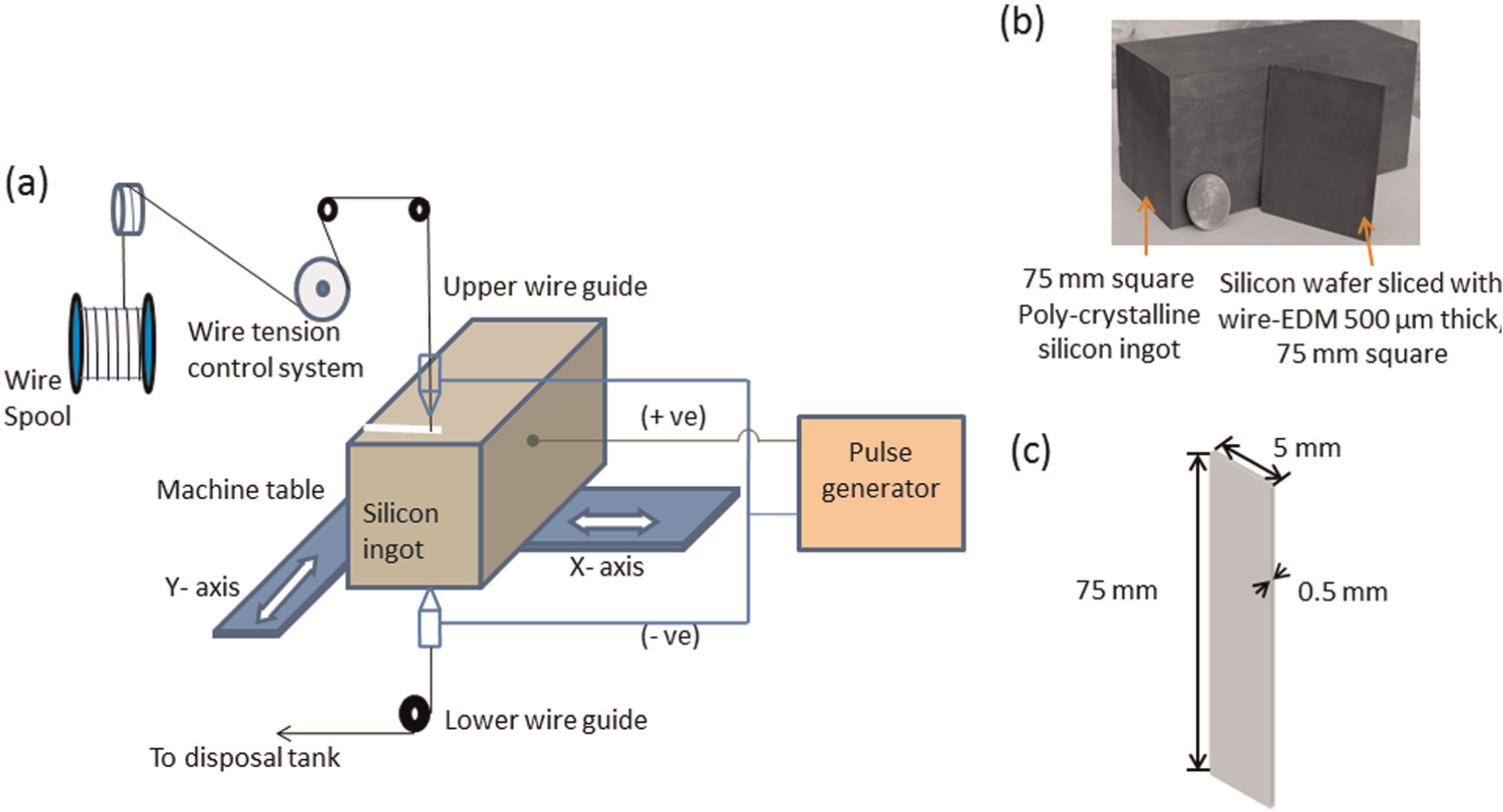
Experimental setup for silicon ingot slicing by wire-EDM: (a) schematic diagram, (b) photograph and (c) schematic representation of silicon wafer sliced during experimentation.
Furthermore, in this experimental work, slicing speed, kerf width and surface roughness have been considered as the response variables. The slicing speed was calculated knowing the time taken for achieving the desired length of cut, as given in the following
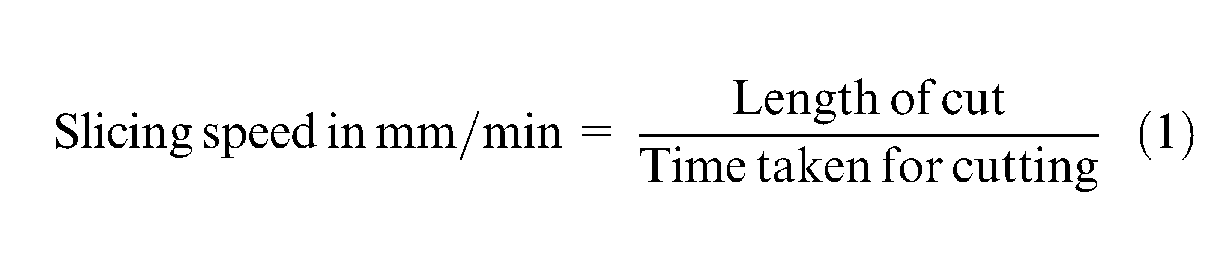
The length of cut was measured by a Tool Maker’s microscope (Nikon-400), and the time taken for cutting a wafer was measured during the cutting operation. The kerf width was again measured using a Tool Maker’s microscope at three different locations—top, middle and bottom—of the slot cut by wire-EDM. Measurement of the surface roughness was carried out by using three-dimensional (3D) optical profilometer (white-light interferometer) Wyko NT9100. Figure 2 shows the theme of the experimental study.
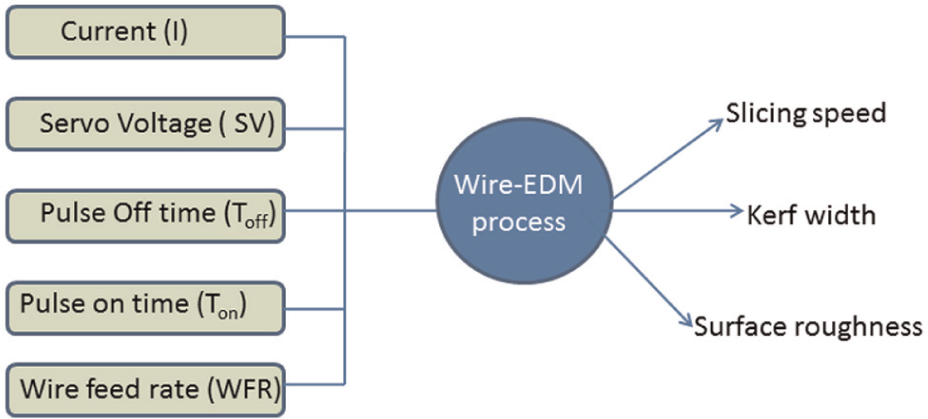
Theme of experiments.
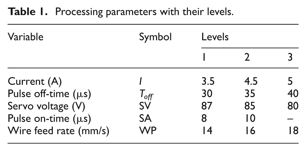
Various levels of processing parameters used during the experiments are given in Table 1. The experiments were performed using constant parameters—wire tension of 3 N, conductivity of dielectric water as 3 µs and water pressure at 10 kg/cm2. All the experiments were repeated once to include repeatability in the analysis of results.
Processing parameters with their levels.
A real-time interelectrode gap voltage and current were measured with a Tektronix TPS2014 digital oscilloscope with 1.0 GS/s sampling rate during the wire-EDM process. The V-I pulse measurement uses P2220 voltage attenuation probe and A622 alternating current/direct current (AC/DC) current probe. At least 7–8 sets of readings were recorded during each experiment.
Parametric effects
Effect of processing parameters on slicing speed
Figure 3(a)–(e) gives the effect of processing parameters on slicing speed. The results show good repeatability as very little variation in error is observed during repeated experimental trials. It is observed from Figure 3(a) that slicing speed increases with the current as the energy of sparks increases. However, an increase in current above 5 A either leads to wire breakage due to small size of wire (100 µm diameter) used in experiments or leads to breakage of thin wafer (500 µm) due to increase in the energy of sparking. This puts limitation on slicing of thin wafers using 100 µm diameter wires such that low energy must be used for such slicing operation. However, the pulse off-time does not influence the slicing speed significantly (see Figure 3(b)). Figure 3(c) shows that with an increase in pulse on-time, the slicing speed increases. This is due to the fact that with an increase in pulse on-time, discharge energy and duration increase, which leads to the formation of larger size craters. This larger size crater formation leads to an increase in the slicing speed. The maximum slicing speed of 0.36 mm/min was obtained at the pulse on-time of 10 µs; if pulse on-time is increased further, it will lead to either wire breakage or breakage of silicon wafer.
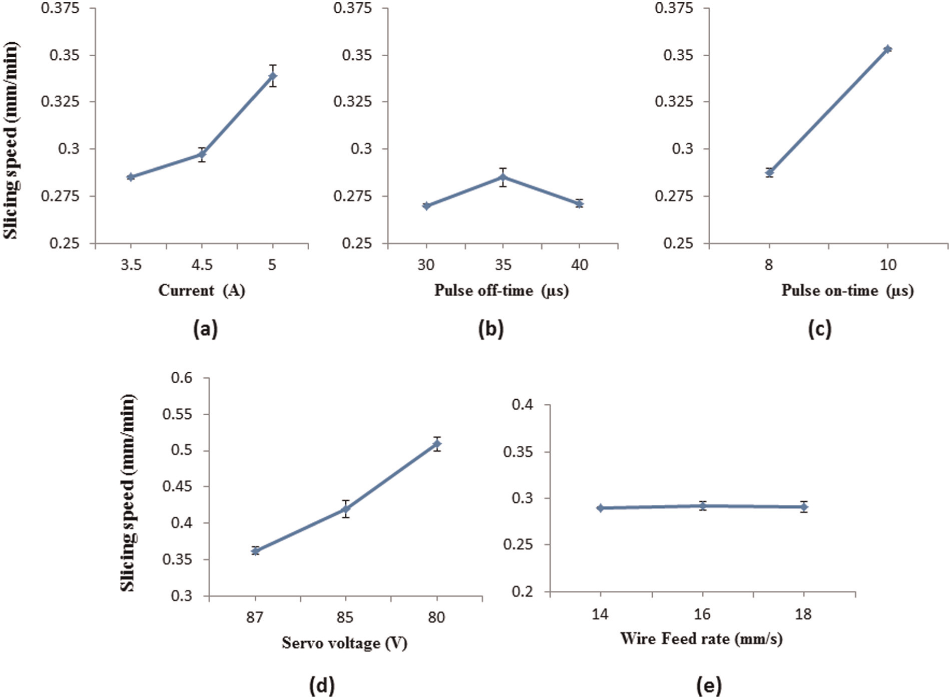
(a–e) Effect of processing parameters on slicing speed.
In order to understand the effect of servo voltage on slicing speed, the phenomenon in a typical pulse cycle has been studied. 15 It is observed that higher servo reference voltage gives longer discharge delay time and hence lower slicing speed (see Figure 3(d)). However, a lower value of the servo voltage gives shorter discharge delay time and higher slicing speed. Similar results were obtained by Shandilya et al. 16 and Wang and Tsai. 17 It is also evident that the servo voltage is the most significant factor affecting the variation in slicing speed. At the 80-V servo voltage setting, it is possible to achieve the highest slicing speed of 0.52 mm/min (see Figure 3(d)). However, it is also observed that if servo voltage decreases below this value, the discharge condition becomes unstable. This is due to an increase in the frequency of discharges for a given time owing to discharge gap being narrow and likely to clog. This will lead to breakage of either wire or wafer due to thin slits. The wafer breaking is additionally compounded due to brittleness of the silicon work material. In silicon ingot slicing, the effect of wire feed rate (WFR) on slicing speed is negligible (Figure 3(e)).
Effect of processing parameters on kerf width
In the PV application, kerf loss is the first important aspect that signifies the cost of wafer manufacturing. As far as the planarity of wafers is concerned, wire-EDM produces a wafer that has planarity in the same range as that of abrasive wire saw cutting process. Therefore, control over the kerf loss becomes an important aspect. In order to analyze this, kerf width was measured at three locations along the cut slot—top, middle and end. The kerf width is given by
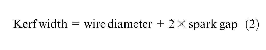
Figure 4 shows a variation in kerf width along the length of cutting. It depicts that kerf width is maximum at middle position, whereas at the top and bottom locations, it is almost identical in magnitude.
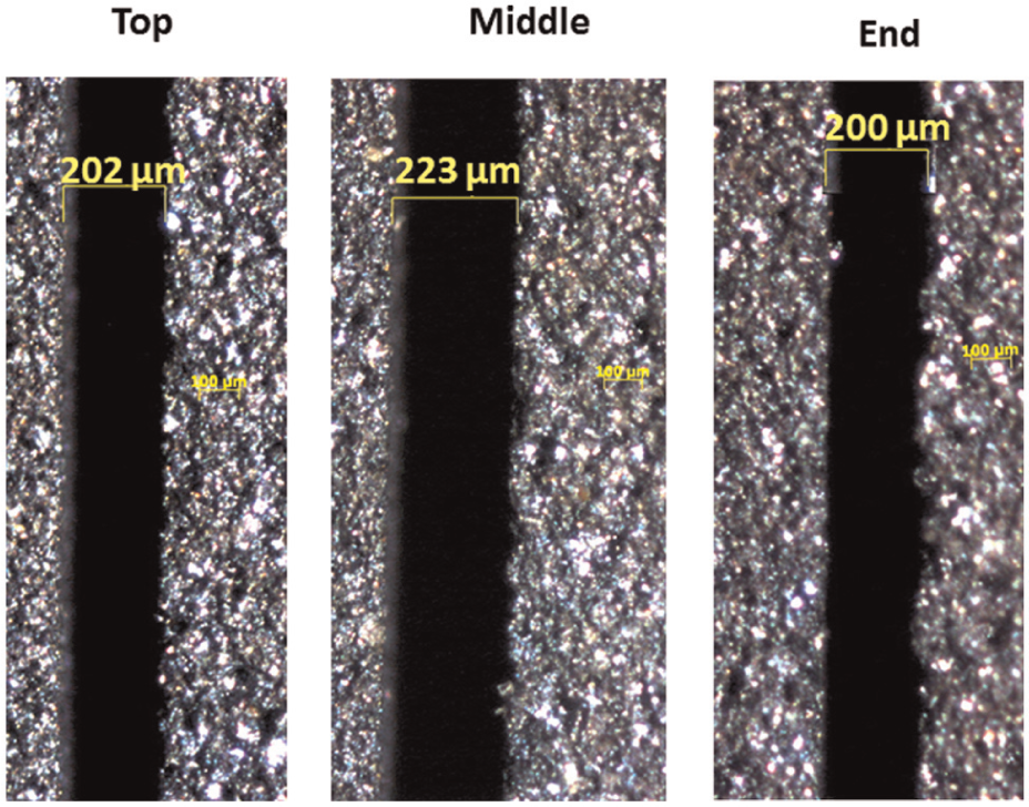
A typical photograph showing variation in kerf width along length.
Figure 5(a) depicts that the kerf width increases linearly with current at all levels, which is attributed to the increase in pulse energy. As observed in Figure 5(b), an increase in pulse off-time from 30 to 40 µs decreases the kerf width by 15%–20%. Generally, it is anticipated that an increase in pulse off-time reduces spark energy and hence the wire vibrations. As shown in Figure 5(c), a decrease in servo voltage from 87 to 80 V shows 5%–10% increase in kerf width. This due to the fact that decrease in servo voltage increases the frequency of discharges and hence the kerf width. It appears from Figure 5(d) that the pulse on-time is a significant factor in increasing the kerf width. As the pulse on-time changes from 8 to 10 µs, an increase in kerf width by 8%–10% occurs. This is due to the increase in pulse on-time and the corresponding discharge pulse energy, which increases the kerf width. The maximum kerf width was observed where pulse on-time was 10 µs. Therefore, in order to decrease the kerf width, a minimum value of pulse on-time of 8 µs must be used. However, pulse on-time below this value gives nonpractical slicing speed, and hence can be used only for finishing cuts. It is clear from Figure 5(e) that WFR appears to have negligible effect on the kerf width. However, it is observed that the kerf width is higher in the middle as compared to the ends of the cross section of the cut. In fact, kerf width is higher at the center of the cut mainly due to wire vibrations, which are mainly due to use of wire of very small diameter (100 µm) and cutting over the silicon ingot of height 75 mm.
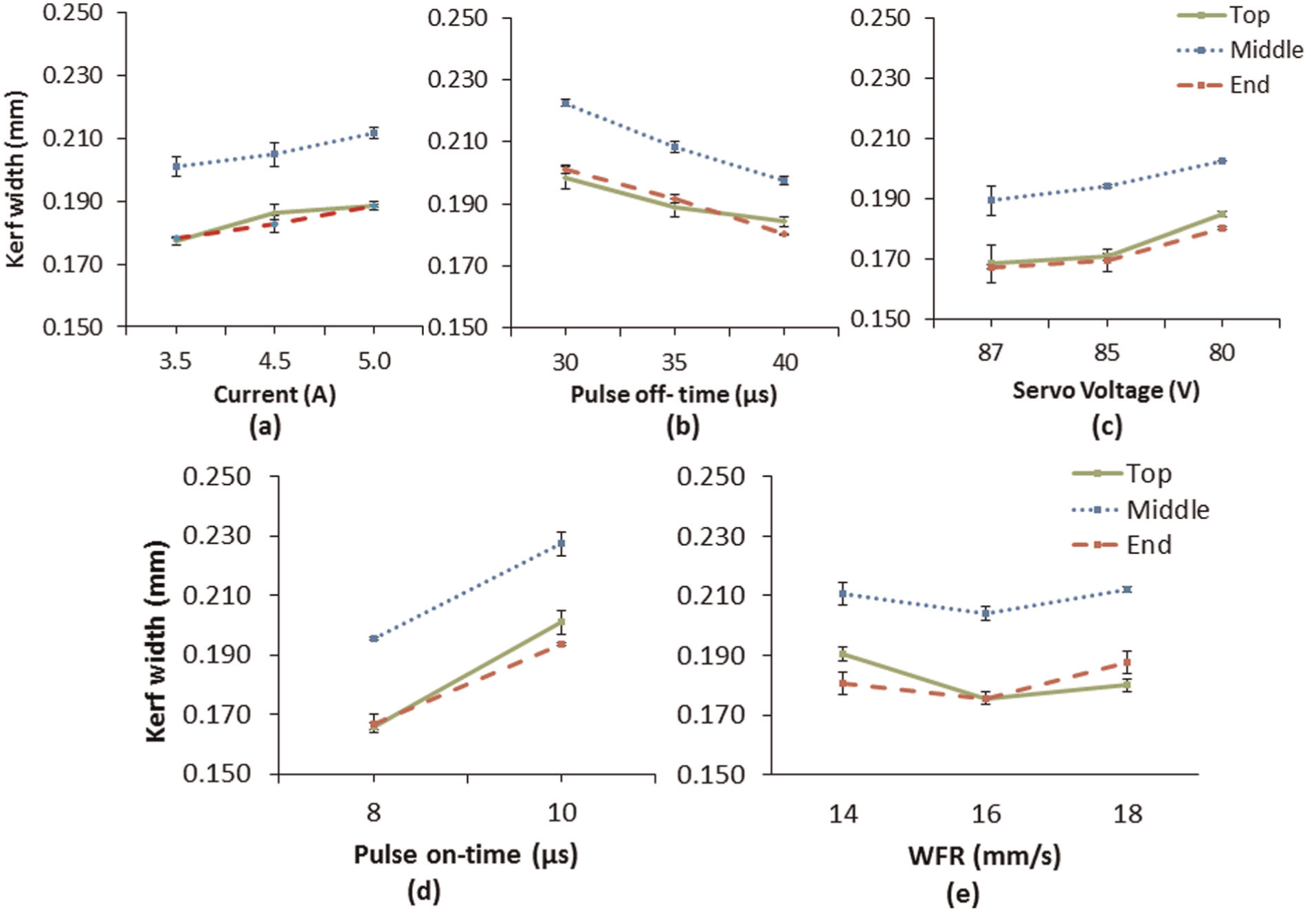
(a–e) Effect of processing parameters on kerf width.
Effect of processing parameters on surface roughness
Surface roughness of the sliced wafer was measured at three locations: top, middle and end. Five readings were taken at each position. Figure 6(a) shows the effect of current on surface roughness. According to this effect, an increase in current from 3.5 to 4.5 A shows a slight decrease in the surface roughness. However, an increase in current from 4.5 to 5 A shows an increase in surface roughness. The increase in surface roughness is due to higher discharge energy causing higher melt depth and larger crater size causing an increase in surface roughness. As shown in Figure 6(b), an increase in pulse off-time from 30 to 40 µs shows a negligible effect on the surface roughness. Figure 6(c) depicts the effect of pulse on-time on surface roughness. It shows that an increase in pulse on-time from 8 to 10 µs causes 10%–15% increase in the surface roughness. At a given current, with an increase in pulse on-time, the energy of discharge becomes higher; the craters formed by discharges become larger and deeper and cause an increase in the surface roughness. As shown in Figure 6(d) and (e), the servo voltage and WFR do not influence the surface roughness significantly. The results show a lot of variation in the surface roughness when the experiments were repeated. The variation could be due to use of single rough cut for silicon ingot slicing, where it is difficult to maintain a particular surface roughness.
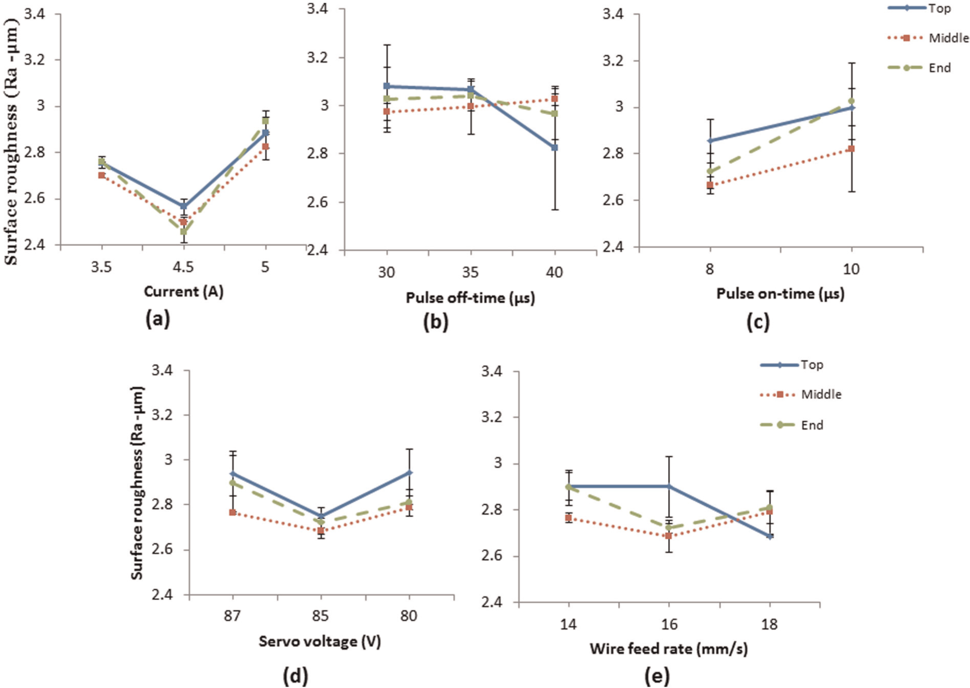
(a–e) Effect of processing parameters on surface roughness.
V-I pulse discrimination
The V-I pulse discrimination is done by obtaining the open and gap voltage values from experimental observations, which are combined with the interelectrode gap current. This information is adequate for discrimination of V-I pulses. As the sampling current data will have disturbances, the threshold value of discharge current was used for analysis. As illustrated in Table 2, gap states are classified as open circuit, off-pulse, normal spark, arc discharge and short circuit by detecting the level of gap voltage and current.
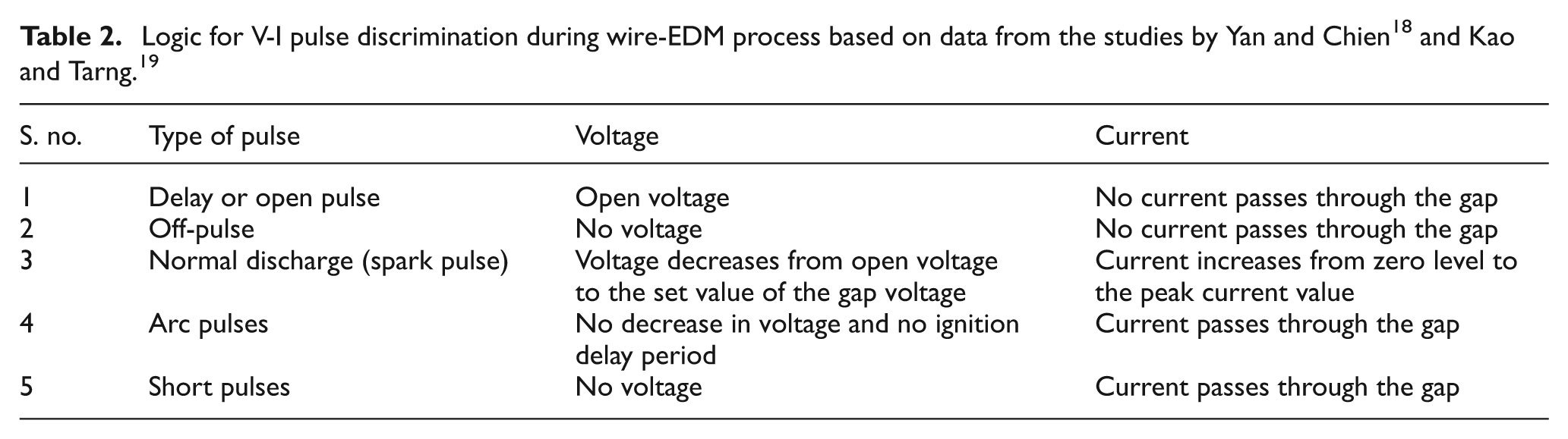
Figure 7 shows a representative V-I waveform obtained during the experiments on wire-EDM machine, which shows discrimination of the V-I pulses based on the logic explained in Table 2. By using the pulse discriminating rules, the types of sparks are divided into the following: No (off-time pulse), Nd (delay pulse), Nn (normal pulse), Na (arc discharge pulse) and Ns (short pulse).
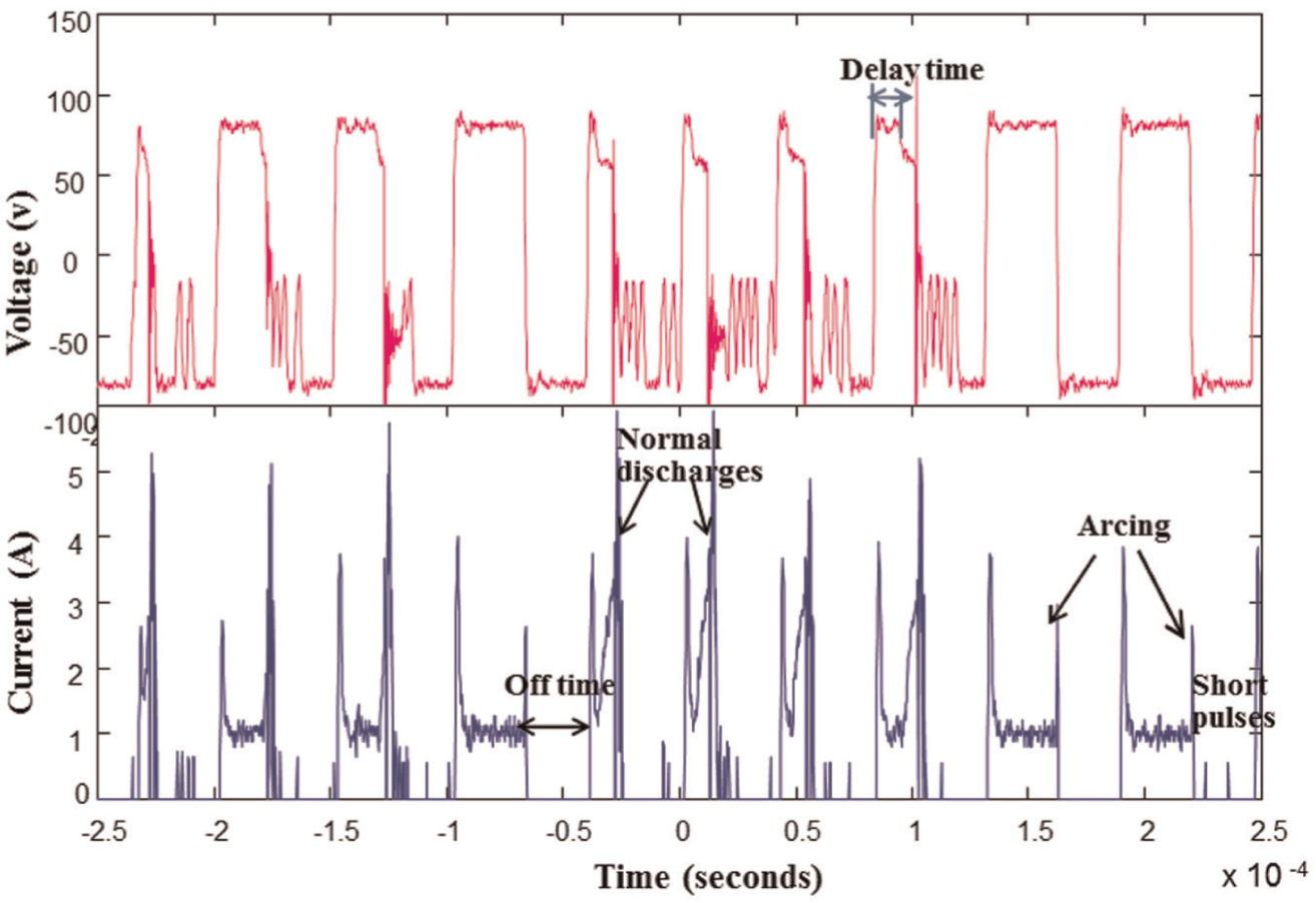
Discrimination of voltage–current pulses.
In a given sampling time T, the proportion of normal sparks in the total sparks defined as normal ratio is computed by Nn/T, off-pulse ratio by No/T, delay period ratio by Nd/T and the arc ratio and short ratio calculated by Na/T and Ns/T, respectively.
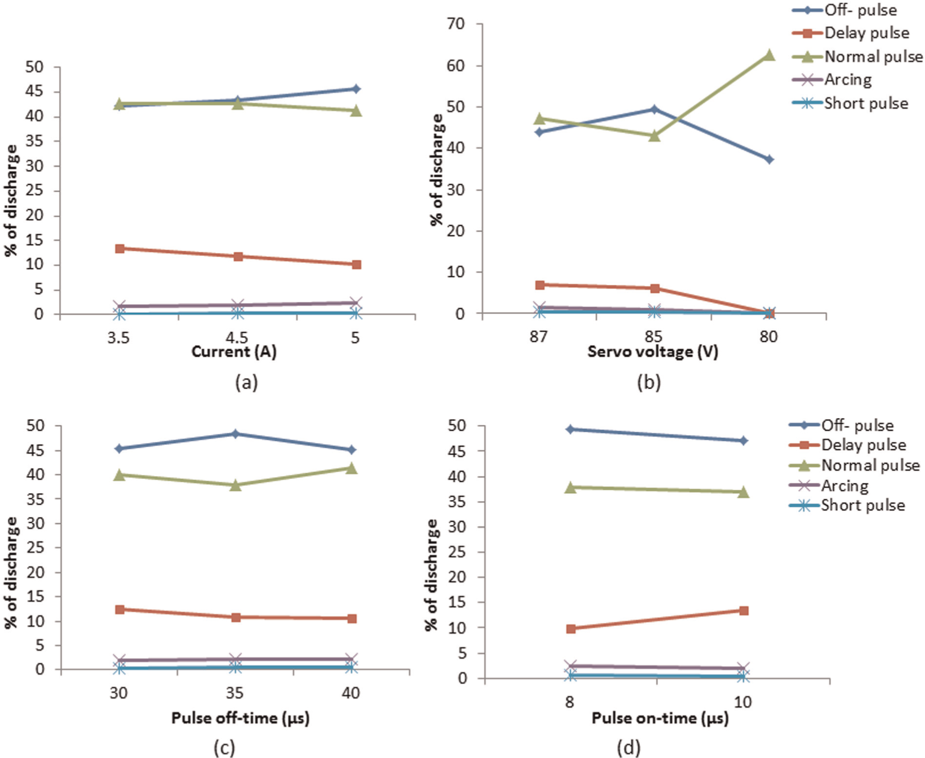
Various types of discharges that occur during wire-EDM process and their variation with respect to processing parameters are given in Figure 8(a)–(d). The discriminated pulses at sampling intervals by voltage and current in wire-EDM process have been studied. The wire-EDM machine, used for experimental work, consists of a device for protection from arcing pulse, which detects the stable arc pulse. Then, the machine immediately postpones the discharge, allowing the dielectric to regain its strength and avoids burning of the workpiece.
(a–d) Influence of processing parameters on pulse discharge type distribution.
To numerically find a correlation between the ratio of pulses and processing parameters, time ratios of pulses computed from a data of V-I pulses are used. All the ratios show weak correlation between the processing parameters and the ratio of pulses. However, an increase in current value from 3.5 to 4.5 A shows a decrease in the delay pulses slightly, hence we get more material removal rate. However, decreasing the servo voltage, the ignition delay time decreases; this is evident from the ratios shown in Figure 8(b). However, the zero ignition delay is not possible practically, but as the data are based on thumb rules, the actual value may be higher than this. An increase in pulse off-time should increase the ratio of off-pulse, which is evident up to the pulse off-time of 35 µs, but beyond this value, the off-pulse ratio decreases due to an increase in the ratio of normal discharge pulse frequency (Figure 8(c)). The effect of pulse on-time shows a major change in off-pulse and delay pulse ratios. As the pulse on-time increases, the off-pulse ratio decreases, whereas the delay pulse ratio increases, as shown in Figure 8(d). As the abnormal discharge ratios are very small, it can be concluded that the occurrence of short pulse and arcing has been taken care of by the machine itself, even though the short pulse can be minimized by properly adjusting the flushing conditions. The occurrence of arc discharges should be minimized as it gives more surface roughness and burning of the workpiece. It is seen that arcing decreases with a decrease in current, servo voltage. As far as the effect of pulse off-time is considered, it observed that there is hardly any change in the arcing ratio with an increase in pulse off-time from 30 to 40 µs. However, slight increase in arcing ratio was observed with a decrease in pulse on-time. The decrease in pulse on-time decreases the discharge energy, which eventually decreases the pressure that is required for debris evacuation. This causes inefficient removal of debris from the gap and results in an increase in the arcing tendency.
The aim of this V-I pulse characterization study was to understand the process mechanism of silicon ingot slicing by wire-EDM by extracting data of current and voltage signals during a discharge. It is found that the nature of the results of V-I data obtained for silicon is similar to that of the steel (HS 6-5-3) as reported by Klocke et al. 20 During wire-EDM, delayed discharges, arcing and short-circuit pulses must be avoided. These discharge forms will reduce the productivity of wire-EDM process and also cause wire breakage. As shown in Figure 8(a)–(d), the percentage of off-pulses and normal discharge pulses is similar. In order to improve the cutting speed, the off-pulse percentage must be reduced. In the same way, the percentage of delayed discharge should be minimized. However, delayed discharges are required for the occurrence of normal discharges. Therefore, in order to improve the slicing rate, proper selection of discharge percentages is needed.
Analysis of machined surface topography
It is understood that the surfaces generated by wire-EDM process must be free from subsurface damage and wire material contamination. This section gives an overview of the characterization of wafers sliced by wire-EDM process. Due to localized heating and rapid cooling of wafer surfaces during sparking in wire-EDM process, a multilayered surface is created. It consists of three layers: recast or white layer being the top most, followed by heat-affected zone (HAZ) and a transformed layer, where a changed grain structure appears. 21
In the case of silicon wafers used for PV cells, the damaged layer must be removed either by polishing or etching. The polishing is usually done using abrasives such as silicon carbide, alumina or diamond with a lubricant to achieve the mirror-like finish. The larger the depth of the damaged layers, the greater the polishing efforts required.
Analysis for depth of thermal damage
In order to characterize the thermal damage, the damaged work surface cross sections on wafers were examined under scanning electron microscope (SEM). This helped quantify the depth of damage. Figure 9(a) and (b) shows typical SEM photograph of the silicon wafer cross sections sliced using various parametric conditions. In order to obtain the minimum thermal damage that is in the range of 10 µm, energy must be minimum. In this case, minimum damage is obtained at current = 3.5 A, Ton = 8 µs, Toff = 40 µs and servo reference voltage = 90 V. Table 3 presents the amount of thermal damage on wafer surface due to wire-EDM at different regimes of energy parameters. As the energy parameters pulse on-time and current increase, the thermal damage also increases. At the same time, an increase in pulse off-time from 35 to 40 µs shows a decrease in the thermal damage from 8.8 to 6.7 µm. However, the slicing speed at these processing conditions will be minimum at 0.28 mm/min. A balance between the slicing speed and depth of thermal damage must be maintained in order to achieve moderate productivity by minimizing depth of damage. The smaller the depth of damage, the lower the polishing efforts after slicing of silicon wafers.
Overview of investigated regimes and resulting thermal damage.
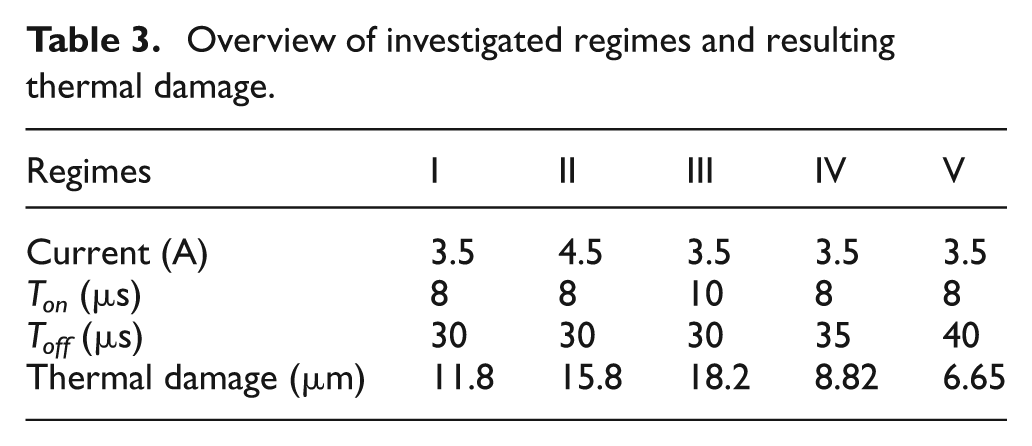
SEM images showing thermal damage of silicon wafers: (a) current = 3.5 A, voltage = 90 V and Ton = 8 µs and (b) current = 5 A, voltage = 90 V and Ton = 10 µs.
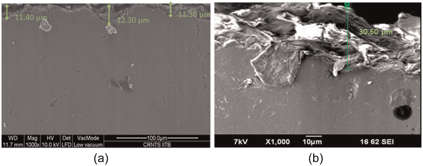
To this end, it may be noted that the wafers cut by wire-EDM are free from saw marks, abrasives marks and microcracks that are often visible in the mechanical abrasive slicing by the linear and wire saws (see Figure 10). Thus, wire-EDM is beneficial in terms of this viewpoint. However, it shows thermal damage on the sliced surfaces. The measurement of thermal damage presented through microscopy shows that the extent of the thermal damage in wire-EDM and the mechanical abrasive processes is more or less identical.
SEM photographs of silicon wafer: (a) wire sawn surface and (b) wire-EDM surface.
Identification of material removal mechanism
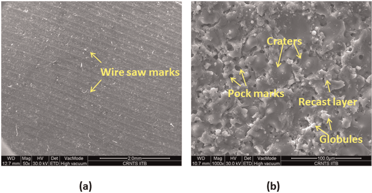
Generally, during EDM, three types of material removal mechanisms occur: melting/evaporation, spalling and oxidation/decomposition. 22 Figure 11 shows surface topography of silicon wafer machined by wire-EDM process in deionized water. The figure indicates regularly formed craters, and no evidence of foamy or porous layer is observed. The surface shows that melting and evaporation are the most dominant material removal mechanisms. It is unlike the ceramic materials, which show formation of foamy or porous layer indicating oxidation/decomposition being the dominant material removal mechanism. Furthermore, the surfaces do not show the presence of large microcracks or irregularly shaped craters which, usually considered as an evidence of thermal spalling, is a mechanism usually observed in EDM machining of ceramics at higher energy levels. 23
SEM photograph of silicon wafer surface machined by wire-EDM.
Thermal erosion model for wire-EDM
Various analytical models for EDM and wire-EDM based on electrothermal concepts have been presented in the literature. There are, however, very few models available to characterize the wire-EDM process. In most of the process modeling studies, a steady-state single-spark phenomenon has been considered. Therefore, this work presents a comprehensive model of the wire-EDM cutting process considering moving line heat source–type nature of the process especially on “difficult-to-machine” materials like silicon. A mathematical model of the erosion process in wire-EDM and predication of consequent temperature distribution in the work surface and erosion rate based on the temperature distribution have been carried out.
Approach to the problem
The approach to determine the workpiece temperature distribution and erosion rate (material removal rate (MRR)) is presented in Figure 12. The proposed model uses moving line heat source with transient temperature distribution. It emphasizes the evaluation of erosion rate during a single pulse on-time assuming that no heat transfer takes place during pulse off-time. The model evaluates the temperature distribution around the silicon ingot and predicts the erosion rate.
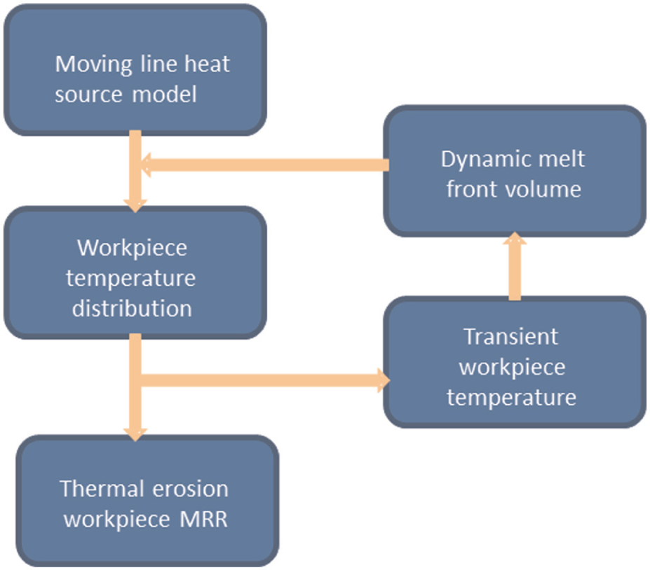
Approach to thermal erosion model.
Assumptions in the model
Wire tool
The wire cross-sectional shape is considered to be circular. At the same time, no lateral displacement of the wire is considered to occur during the cutting operation.
Workpiece
Workpiece material is considered to be ‘infinite’ and isotropic with respect to thermal and mechanical properties.
Melt pool
Entire melt pool volume formed during pulse on-time gets eroded. This corresponds to the flushing efficiency of 100%. Furthermore, the erosion is completed at the end of the sparking time or pulse on-time.
Erosion
The erosion of work material is symmetric on both sides of the wire.
Latent heat
The latent heat absorbed during melting and evaporation has not been taken into account in the model, as these considerations in EDM do not affect the estimation of the erosion rate of the workpiece by more than 2%.24,25
The various thermal properties of polycrystalline silicon considered for modeling are as follows: melting point = 1680 K, specific heat = 0.7 J/(g °C), thermal conductivity = 148 W/m K and thermal diffusivity = 0.8 cm2/s.
Figure 13(a) explains the cutting system wherein wire tool advances to cut in the direction along y-axis with a velocity vf. The axis of wire is z-axis and is into the plane of the paper, while x-axis lies in the plane of cut. The workpiece area surrounding the wire melts, and the erosion rate is determined by the volume of workpiece eroded per second. Figure 13(b) displays a schematic of fixed and moving coordinate system for moving point heat source.
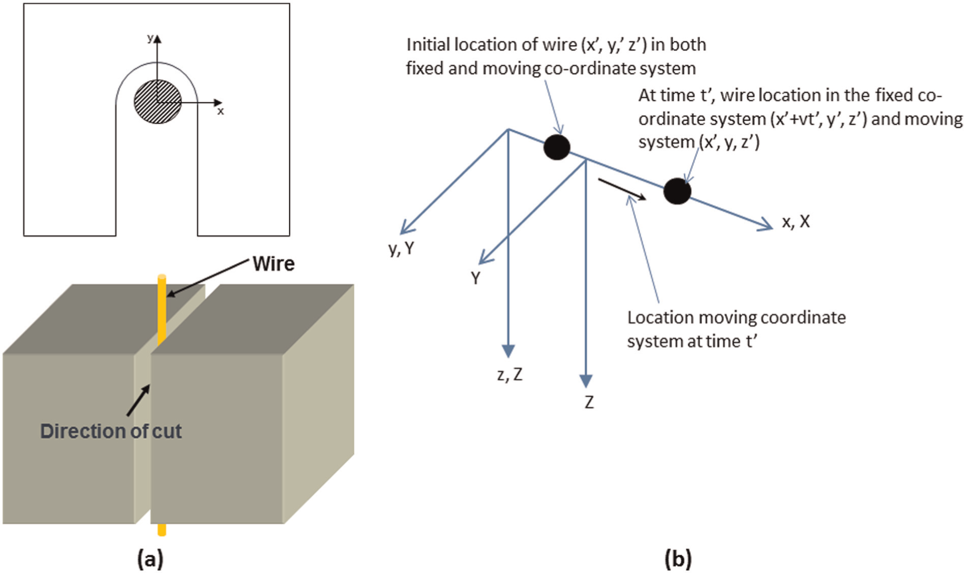
(a) Moving line heat source cutting the workpiece and (b) schematic diagram of moving point heat source.
Model formulation
The differential equation of heat conduction in fixed coordinate system for a point heat source is given as26,27
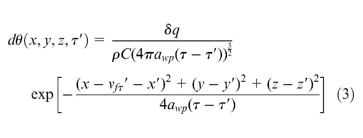
In a moving coordinate system (see Figure 13(b)), the equation for a moving point heat source solution can be written as
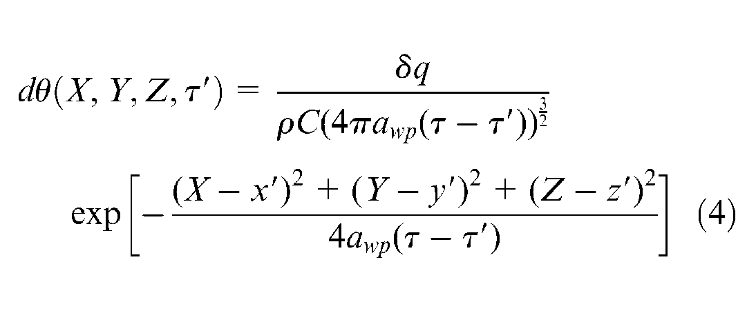
where δq is the amount of heat released in an infinitesimal time increment dt′(δq = Pdt′) at instantaneous location (x′, y′+ vf.τ, z′) at time τ.
The temperature distribution for infinitely extended isotropic body with time-dependent moving line heat source is given in equation (5)
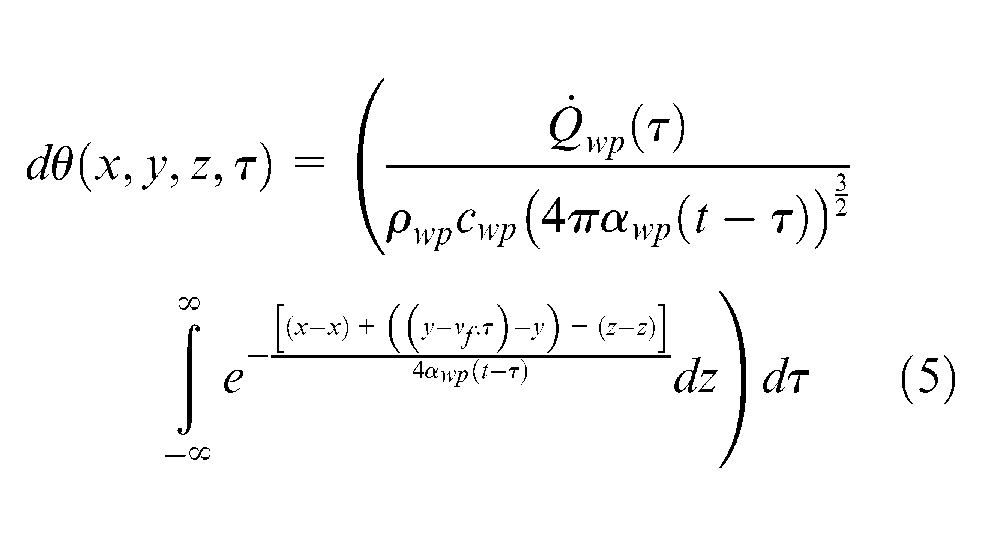
Integrating the above equation gives equation (6) 28
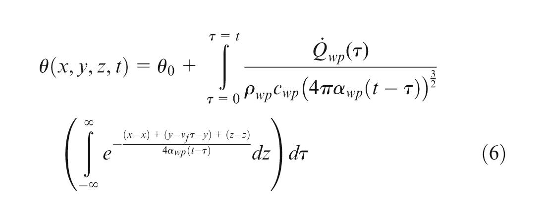
In the uniform heat source,
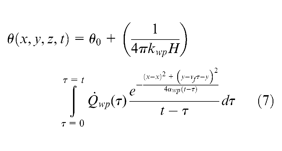
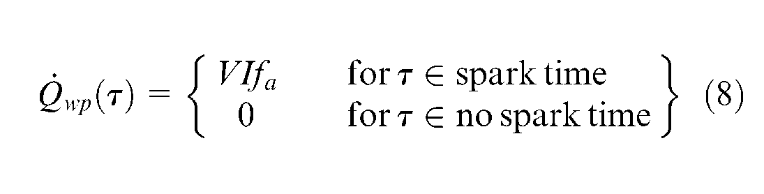
In the case of wire-EDM process, the time dependence occurs due to use of a pulsed cycle. The duty cycle consists of alternate sparking and nonsparking periods. Hence, for an input current “I” and the interelectrode voltage “V,” the heat input rate
Here, it has been assumed that the current and voltage do not change during both periods of a duty cycle.
The numerical solution of equation (7) is given in equation (9)
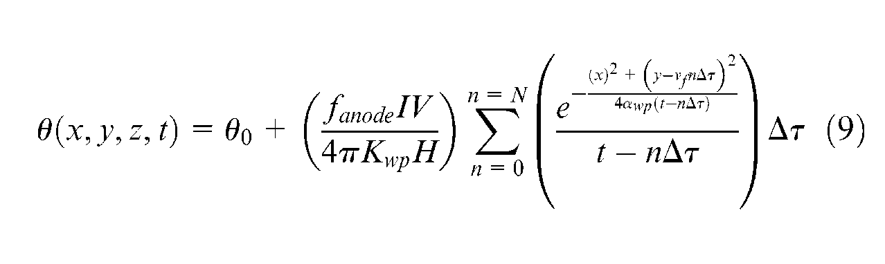
The above relation has been used to determine temperature distribution in the silicon ingot during wire-EDM as a moving line heat source as a function of heat input during pulse on-time.
Model evaluation
The moving line heat source model evaluation is conducted by writing a program using MATLAB. In the model equation, it is assumed that heat transfer takes place during pulse on-time and with the heat input rate of “
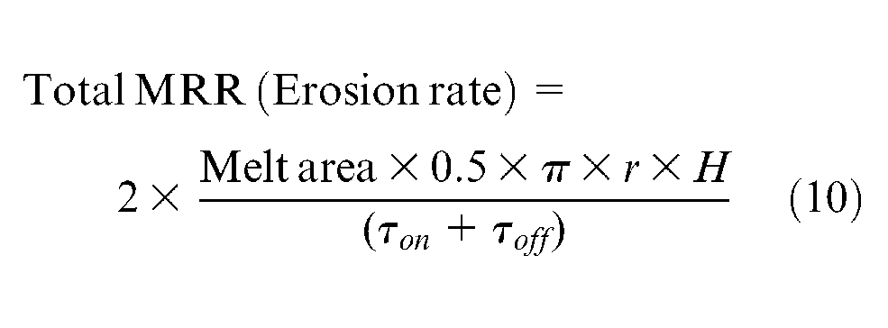
where “r” is the radius of wire + spark gap and “H” is height of the job. The total MRR is obtained by multiplying it by 2 as the simulation is for quarter circle.
Model results
The results of temperature distribution are shown in Figures 14 and 15. Figure 14 represents temperature distribution plot of the workpiece for a quarter of the wire–workpiece contact region at the end of the pulse on-time. The melt pool is the volume of the workpiece where the temperature exceeds the melting point of material that is 1680 K.
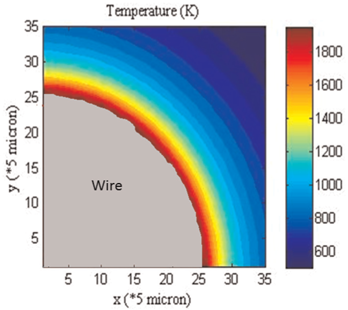
Spatial workpiece temperature distributions.
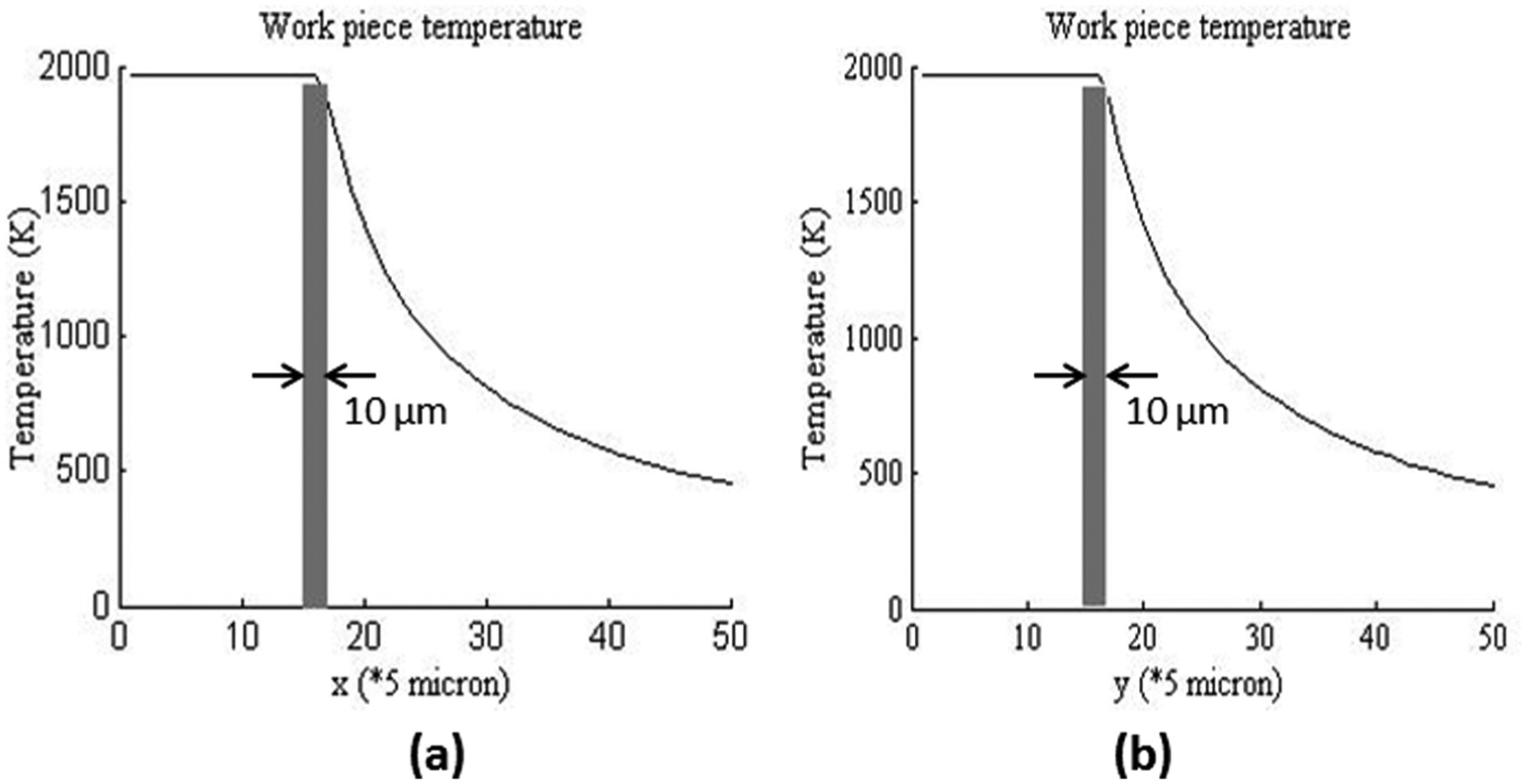
Workpiece temperature (K) as a function of (a) x-axis coordinates and (b) y-axis coordinates.
A variation in workpiece temperature with x-axis is shown in Figure 15(a), at the processing conditions Ton = 8 µs, Toff = 30 µs, current = 3.5 A, servo voltage = 87 V and WFR = 14 mm/s. The shaded region in the graph depicts the melt pool cross section in this region, which is approximately 10 µm in width. A variation in workpiece temperature with y-axis is shown in Figure 15(b). The shaded region in the graph depicts the melt pool cross section in this region, which is again 10 µm in width. The areas of shaded regions in Figure 15(a) and (b) are almost identical as the wire advancement velocity is very low and is ≈10 µm/s.
In the model for wire-EDM of Si ingots, the parameters observed to affect process performance are current, voltage and wire velocity. Out of these parameters, current and voltage have been combined to consider power as a parameter in the models. Wire velocity is the rate at which the wire moves in the direction of machining. This velocity has been fixed because the rate of advancement of the wire depends on the ingot erosion rate and hence cannot be determined unless the ingot erosion rate is known. To support the choice of a fixed rate of advancement of the wire, the moving heat source model was employed with a varying wire advancement rate. It was evident that the advancement rate did not affect the melt pool significantly within one spark on-time for a practical range of parameters. Hence, it was fixed at 100 µm/s. A common wire material, brass, has been used in all the calculations.
Figure 16 shows a variation in transient workpiece temperature of a point (135 µm, 135 µm) due to a variation in the effective power supplied during erosion. The effective power is the percentage of power used for causing the workpiece erosion. The workpiece temperature at a point increases with the input power as a result of increased energy of sparking.
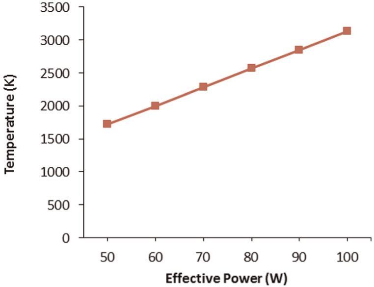
Effect of power to the transient temperature.
Experimental validation of the erosion model
To validate the model, the erosion rate of wire-EDM of silicon ingot was compared with experimental results. In this experiment, a 100-µm brass wire was used as a wire electrode and 75-mm square poly-silicon ingot as work material. The MRR obtained from the erosion model described in equation (10) was compared with the experimental values of MRR. As current increases, the experimental and simulated erosion rate increase (see Figure 17). The error in MRR predication is in the range of 15%. The MRR predication accuracy may be improved by using temperature-dependent properties of the work material and also by including spatial sparking distribution coupled with using moving volume heat source.
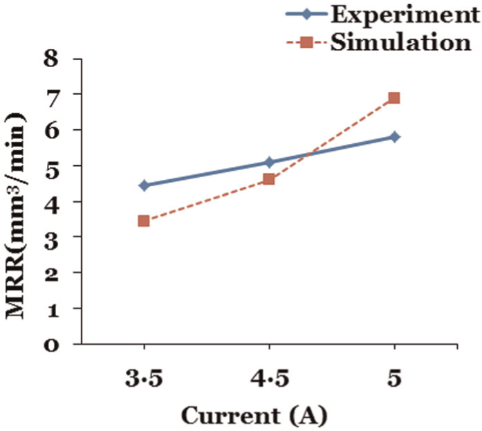
Experimental validation of thermal model.
Conclusion
This experimental analysis has shown that wire-EDM is a promising process for silicon ingot slicing. It is observed that the metal removal rate in slicing of silicon ingots is 30%–40% higher than the conventional slicing methods such as ID saw and single-wire abrasive wire saw. Based on this experimental work, the following conclusions are made:
Slicing speed is mainly influenced by the energy parameters such as current, voltage and pulse on-time. Out of these, servo reference voltage is the most significant factor.
Kerf loss is mainly governed by the pulse on-time and servo reference voltage; it shows maximum kerf width at middle of the cut, which is due to wire vibrations. Efforts must be made to minimize the amplitude of wire vibrations in order to achieve better planarity on the machined wafer.
Surface roughness does not vary significantly with the variation in processing parameters. However, it was observed that surface roughness can be minimized by decreasing the energy parameters such as current, voltage and pulse on-time.
This article also proposes model for calculation of erosion rate, and it calculates the temperature profiles by considering wire as a moving line heat source. This temperature profile gives a melting zone, which is assumed to be the final eroded cavity dimensions. Major conclusions based on this modeling work are as follows:
The simulation of the wire-EDM process of silicon ingot slicing shows that transient temperature distribution of the workpiece can be use to predict the erosion rate.
The model helps to obtain an optimum duty cycle, which facilitates obtaining higher erosion rate.
The experimental validation of the model shows that it matches with the experimental values with reasonable accuracy of 20%.
Footnotes
Appendix 1
Acknowledgements
The authors thank National Centre for Photovoltaic Research and Education (NCPRE), IIT Bombay and Mitsubishi EDM/ Laser / MC Craftsman Machinery Pvt. Ltd, Chennai for permitting us to use their facility to undertake this experimentation.
Declaration of conflicting interests
The authors declare that there is no conflict of interest.
Funding
This study received from National Centre for Photovoltaic Research and Education (NCPRE), IIT Bombay sponsored by MNRE, Government of India.