
Abstract
The use of additive manufacturing (AM) or 3D printing in sensor technology is increasing daily because it can fabricate complex structures quickly and accurately. This study presents the modeling, fabrication, and characterization processes for the development of a resistance type flexible strain sensor. The finite element model of the sensor was developed using COMSOL software and was verified experimentally. The experimental results agreed well with the simulation results. The fabrication process was performed using the molding technique. The flexible substrate of the strain sensor was fabricated by fused deposition modeling (FDM), an AM method, with dimensions of 20 mm × 60 mm and a thickness of 2 mm. In this process, a flexible and durable elastomer material called thermoplastic polyurethane (TPU) was used. The liquid conductive silver was then injected into the mold channels. The characterization process was performed by establishing experimental and numerical setups. Studies were conducted to maximize sensitivity by changing the geometric properties of the sensor. At the 30% strain level, sensitivity increased by 9% when the sensor thickness decreased from 2 to 1.2 mm. As a result of the gradually applied force, the strain sensor showed a maximum displacement of 34.95 mm. Tensile tests were also conducted to examine the effects of stress accumulation on the flexible base. The results of this study show that the strain sensor exhibits high linearity-sensitivity and low hysteresis performance.
Keywords
Introduction
Additive manufacturing (AM) or 3D printing technology is the process of physically producing a model designed in a computer environment using a printer. 1 This technology, which is in constant development, has made progress in various sectors, such as medicine, aviation, robotics, space, wearable technologies, automotive, and sensors.2–4 AM is a fabrication method that offers advantages, especially by providing flexibility in fabrication processes. 5 In this method, the product is built in layers using material layers or additions. In this way, the fabrication of parts with complex geometry becomes easier, rapid prototyping is enabled, and design freedom is increased. 6 Additionally, reduced material waste contributes to lower fabrication costs. 7 AM offers an effective solution, especially for the fabrication of customized products and small-scale mass production. The integration of AM and sensor technologies can make manufacturing processes more flexible, thereby increasing the ability to respond quickly to design changes. 8 It can also reduce energy and material waste, making fabrication processes more sustainable. This integration can provide smarter and more competitive production by creating a production environment that complies with industry 4.0 principles. 9
AM technology has led to increased interest in the fabrication of flexible sensor devices.10–12 These devices include strain sensors with excellent stretch ability and compatibility, which are highly desirable in applications that need to measure large deformations, such as human-machine interface interactions, health monitoring, robotics and automotive.13–15 Strain measurements are essential for monitoring mechanical systems from both static and dynamic perspectives. These sensors are structures that measure the deformation caused by at force applied to a material and convert this information into electrical signals. Strain sensors play an important role in industrial applications in evaluating the mechanical properties of materials, performing structural analyzes, and performing durability tests. 16 The most important of these sensors is the resistive strain sensor developed in this study. The sensor uses a flexible substrate combined with an electrical conductor to allow a change in the electrical resistance due to mechanical deformation in the flexible substrate.
Strain sensors are generally fabricated by traditional methods, such as planar printing, soft lithography, and chemical vapor deposition to create sensing circuitry on flexible substrate.17–19 These mass fabrication methods must operate in a clean room, do not support small-batch customization, and require additional assembly steps that reduce the structural integrity of the fabricated strain sensors.20–22 Therefore, there is a critical need for an easy and efficient approach to directly and reliably build flexible strain sensors in objects. Among AM approaches, fused deposition modeling (FDM) is one of the most widely utilized methods, offering significant potential for the fabrication of flexible strain sensors. 23 This is attributed to its widespread availability, rapid design iterations with minimal material waste, high production rate, and cost-effectiveness.24,25 In particular, the multi-material FDM technique enables products with material, structural, and functional complexity to be realized in a single procedure. 26 The proposed technique enables the application of electrically conductive materials in multi-material FDM, paving the way for the development of flexible strain sensors. To this end, numerous researchers have effectively demonstrated the utilization of FDM for manufacturing flexible strain sensors.27–29
Strain sensors can be fabricated from different materials, depending on the requirements of the particular industry or application.15,30,31 Conductors used as filling materials in these sensors include carbon nanotubes, graphite, liquid metals, and conductive polymers.32–34 The flexible substrate of the sensors is fabricated from materials, such as thermoplastic polyurethane (TPU), ecoflex, and rubber.35,36 In this study, a flexible strain sensor was fabricated using the molding technique. The flexible substrate of the sensor was fabricated using FDM method and TPU material. The detection traces were created by injecting a liquid conductive silver material, and the manufacturing process of the strain sensor was completed.
In previous studies, there has been a growing interest in the fabrication of flexible strain sensors and a serious need for their use.37–39 To this end, the current study aims to conduct numerical and experimental studies to analyze and characterize the performance of strain sensors by producing strain sensors using 3D printing, a modern fabrication technique. This study originates from soft and flexible materials, which are a reference for the fabrication of strain sensors with different designs and properties, with the advancement of AM technologies. Because these sensors contain electrical and mechanical components, not only their mechanical behavior but also electrical behavior must be characterized. Previously developed sensor models do not consider the nonlinear behavior of materials. As a result, a mismatch occurs between the theoretical predictions and the experimental data during the characterization process. Therefore, it is necessary to develop an experimental process that provides a full characterization to analyze and optimize continuously evolving strain sensor structures. To the best of the authors’ knowledge, few studies have numerically examined,40,41 but there are sensor studies with different designs, models, and manufacturing processes.42–44 Elgeneidy et al. worked on a fully printable strain sensor bending actuator that can be calibrated to provide bending feedback and simple contact detection. 45 The sensor was directly fabricated in 3D using easily accessible FDM printer hardware. The flexible strain sensor was directly welded to the body of the bending actuator and systematically tested to characterize and evaluate its response under varying input pressures. The results of this study demonstrate how the FDM printing process can be tuned to directly print customizable strain sensors that provide reliable bending feedback and basic contact detection. Ertugrul et al. presented the fabrication and experimental studies of a 3D printed strain sensor that can be used in soft applications. 46 Stereolithography (SLA) based 3D printer was used for fabrication. The bottom base of the sensor, which consists of two parts, is made of flexible UV resin, and the channels that should be conductive are made of conductive UV resin. Experimental studies were conducted under loading and unloading conditions to observe the hysteresis effect of the sensor. The results showed a close linear relationship between the strain sensor and the measured resistance. Lim et al. fabricated graphene-based strain sensors with different slicing angles using FDM and systematically examined the effect of strain angle on the performance of graphene-based sensors. 47 The alignment of graphene filaments with respect to the direction of applied strain was found to affect the gauge factor (GF). The results showed that the 45° pattern exhibited higher sensitivity and stability than the 180° pattern, whereas the GF was larger for the 180° pattern. Maurizi et al. investigated smart 3D structures with embedded and printed sensory elements. 48 The embedded strain sensor was based on conductive polylactic acid (PLA) material. The research focused on dynamic measurements of strain and took into account the theoretical background of piezo resistivity of conductive PLA materials, temperature effects, nonlinearities, dynamic range, electromagnetic sensitivity, and frequency range. It has been shown that the sensory element is linear as long as the structure has a linear response, the dynamic range starts at ∼30 µc, and the broadband performance is in the range of several kHz.
In this study, a prototype of single-axis strain sensor was fabricated using the FDM method with dimensions of 20 mm × 60 mm and a thickness of 2 mm. The electromechanical finite element model of the sensor was constructed using COMSOL software. The characterization process was performed by establishing experimental and numerical setups. These model results were compared with the real-time characterization experiment results, and the results were found to be in good agreement. Thus, the characteristics of the resistive strain sensor are better understood. Additionally, studies were conducted to maximize sensitivity by changing the geometric properties of the sensor. Finally, tensile tests were performed to investigate the effects of stress accumulation on the flexible base. The results of this study provide design guidelines and a roadmap for flexible strain sensors and demonstrate the potential of AM.
Materials and methods
Design of flexible strain sensor
The design of the resistance type flexible strain sensor is shown in Figure 1. This design overlaps with previous strain-gage sensor designs in the literature. The key components of the sensor are U-shaped conductive channels and a flexible substrate. The conductive channel consists of six long and five short channels. The bottom substrate of the sensor is designed from a material with high flexibility and strength called thermoplastic polyurethane (TPU), while the detection traces are designed from liquid conductive silver material. The design of the sensor was carried out in 3D using SolidWorks, a computer-aided design (CAD) software. The 3D model of a strain sensor with a TPU substrate (yellow) and embedded conductive silver tracks (gray).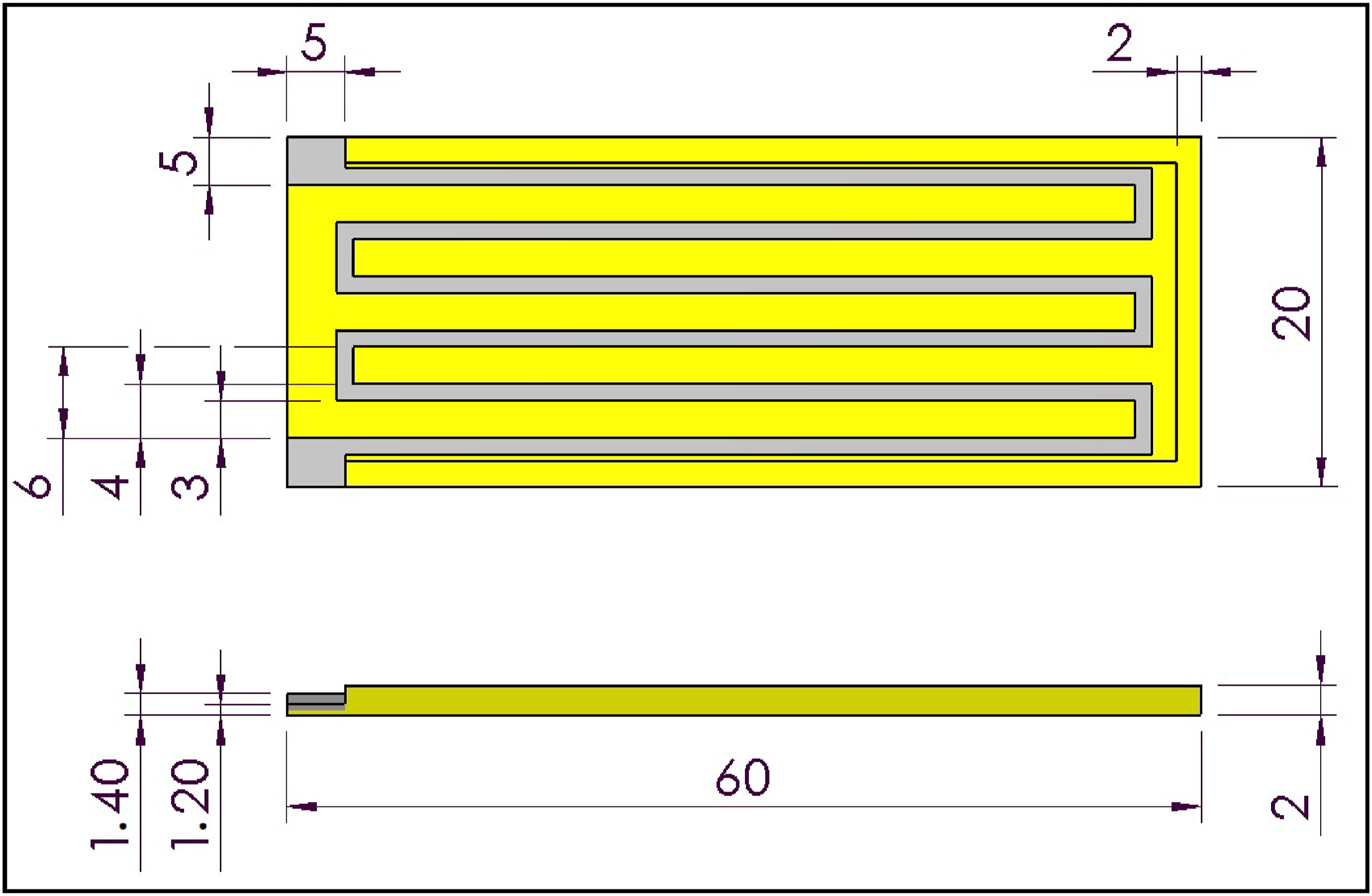
The sensor thickness must be taken into consideration during the design process. Because the main purpose is to ensure sensor flexibility with a flexible substrate and to detect movements using a conductive material. Although the conductive silver material is not very flexible, it becomes flexible enough to stretch when printed at very thin thickness, thus preserving the desired flexibility of the sensor. Therefore, as the flexible sensor substrate elongates under external forces, the thin conductive traces embedded within it also follow the bending, changing the electrical resistance. As a result, the strain values occurring in the sensor can be calculated from the resistance change.
The minimum trace thickness of the strain sensor was determined as 0.4 mm, which is equal to the minimum layer thickness that the printer used for fabrication can print. Therefore, the sensor thickness is only 1.4 mm, and the detection tracks are 0.8 mm. These design dimensions ensure that the sensor remains flexible. Additionally, the ends of the conductive paths are left exposed to facilitate data acquisition via the sensor. In the following stages, to easily apply the sensor to any system, a raised step of height 0.6 mm and width 1.1 mm was added to the top of the sensor, and the total thickness of the strain sensor was 2 mm.
Fabrication process
Sensor design and print settings must be optimized for successful fabrication. Increasing the cross-sectional area of the conductor tracks ensures that they remain functional during sensor extension. Additionally, printer characteristics, such as the nozzle diameter, must be taken into account when determining the dimensions of the detection tracks. Thus, conductive traces can be printed successfully without any over or under-extrusion problems. To obtain smooth results without any inconsistency or intermittent movement in the slicing software used to determine the print settings, the planar dimensions of the sensor were determined to be exact multiples of the nozzle diameter. The vertical dimensions of the strain sensor were also chosen as exact multiples of the layer thickness.
The fabrication process of the flexible strain sensor was performed using “Zaxe Z1 Plus”, a fused deposition modeling (FDM) based 3D printer. In the FDM method, a thermoplastic filament is melted through a nozzle and then deposited onto a 3D area in the desired shape to form a layer by layer. 49 The nozzle moved along X, Y, and Z axes to create each layer of the computer-determined design. Each layer is added one on top of the other to create the final piece. The 3D printer has a nozzle diameter of 0.2-0.8 mm and a printing resolution of 50-400 microns. 50 Thus, it is possible to produce sensors of the desired thickness. This printer is compatible with many filament materials, such as polylactic acid (PLA), acrylonitrile butadiene styrene (ABS), thermoplastic polyurethane (TPU), nylon, conductive, and wood. The materials used to fabricate the strain sensor were Zaxe flex TPU filaments, and conductive liquid silver. The main advantage of TPU filaments is the creation of flexible prints with elastic properties. TPU is a filament that uses a combination of plastic and rubber. TPU is a thermoplastic elastomer material with properties such as flexibility, durability, and strength. 51 It is often used in many different applications, such as 3D printing and industrial manufacturing.
The 3D printer parameters used to fabricate the strain sensor.
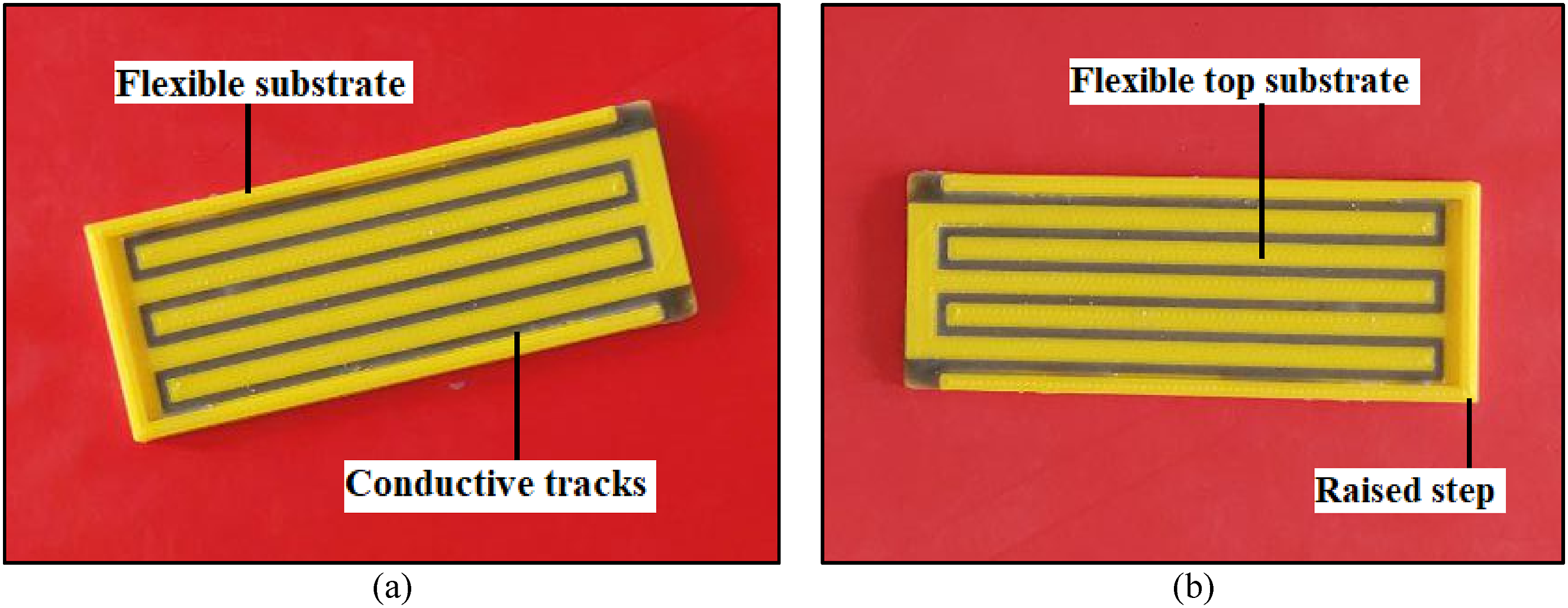
Structure of the 3D fabricated flexible strain sensor (a) Conductive traces printed on a single substrate of flexible material (b) Fabrication after adding the top layer with a raised step.
Sensor wiring process
The key challenge encountered when characterizing the strain sensor during experimental studies was to create a stable wiring interface. The conductive silver material used to print the detection traces cannot be integrated directly into copper or silver wires. Therefore, to measure the resistance of the strain sensor, the wires had to be connected to the sensor terminals. When the cables were attached with the help of metal clamps, the measured electrical resistance of the sensor was very unstable. In addition, the resistance value varied greatly when the cable was moved. This effect occurs because the conductive traces are printed at very thin thickness, which causes vibrations in the printed traces when the cable moves. Thus, the resistance readings measured from the sensor are distorted. A low-cost conductive jumper cable was used to solve this problem. One end of the cable was wrapped around the strain sensor terminals, and hot silicone was applied to secure it (Figure 3). The other end of the conductive cable is wrapped around a metal pin and fixed. As a result, the device can be securely fixed with a lightweight and flexible cable without damaging the terminals or ensuring that the weight of the cable does not affect sensor reading. After installation of the cables, no measurement error was observed in the data measured by the flexible strain sensor due to the movement of the cables. Wiring the strain sensor to the exposed terminals of the conductive threads.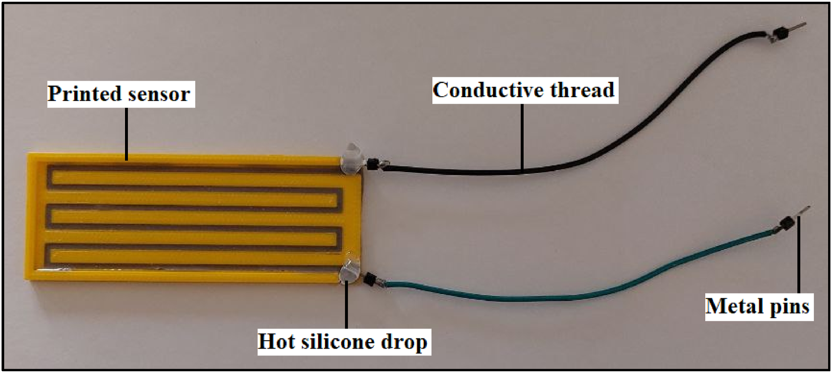
Experimental Setup
The schematic diagram of the experimental setup used to test and characterize the strain sensor, which was completed in the fabrication process, is shown in Figure 4. In this setup, a material testing device with a load cell (ZwickRoell Material Testing Machine) was used to measure the displacement and force of the strain sensor. Measurement data were transferred from the device to the PC using a cable. A circuit was established to measure the changes in the resistance of the strain sensor. The metal pins of the sensor were connected to this circuit; The measured values were transferred to a data collection card. For this purpose, a constant voltage of 5 V was applied through a 180 Ω resistor connected in series to the sensor to increase the measurement accuracy. Because the resistance of the strain sensor is low, heating occurs at resistances below 180 Ω. The voltage drops occurring during the experiment were measured using a multimeter. The strain sensor was placed on the force meter device using a hook. By ensuring that the sensor remained stationary, a multimeter device was attached to the connection terminals of the sensor to measure the voltage drop. Then, a force was gradually applied to the strain sensor. Measurements were recorded for the force, displacement, and voltage, as voltage variations resulted from continuously altering the applied force. As a result of the loading applied to the strain sensor, the length changes in the sensor Experimental setup used to characterize the resistive type flexible strain sensor.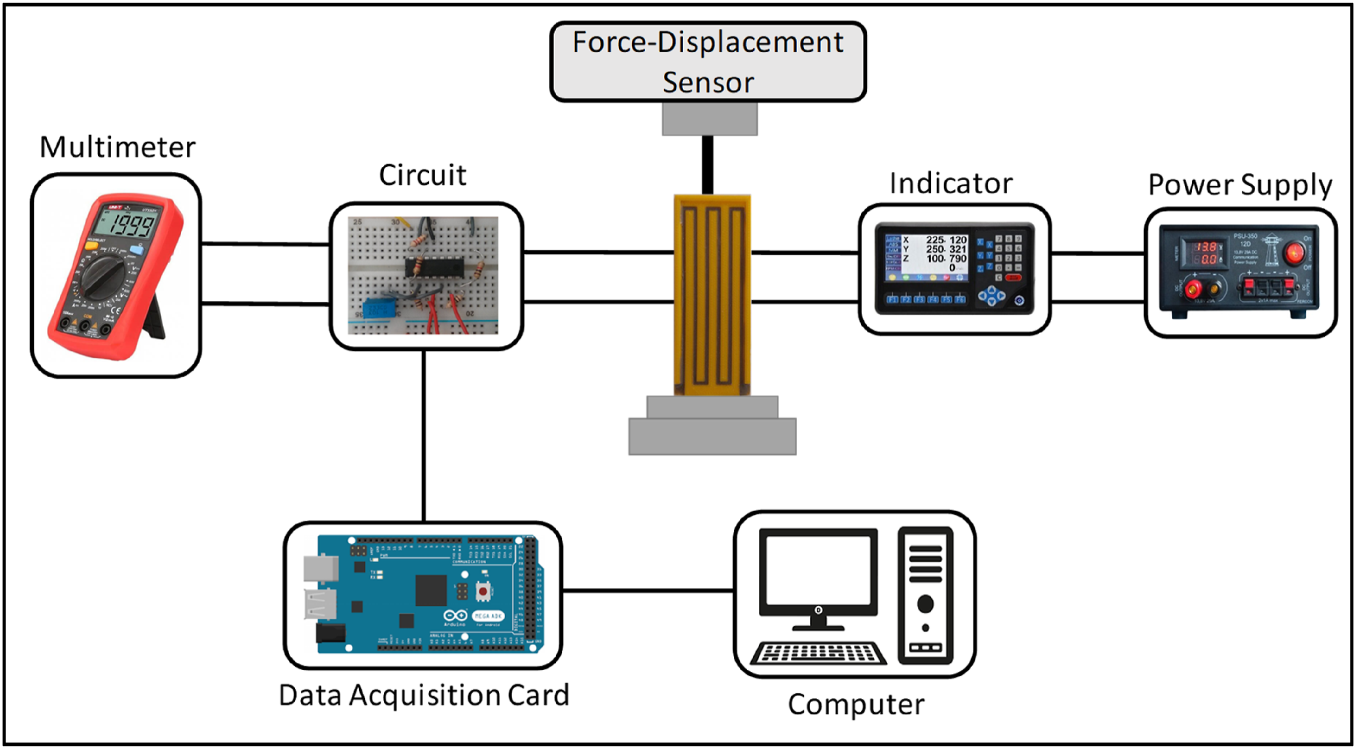
Tensile tests were implemented to examine the elongation of the flexible strain sensor against force. These tests were performed using a cell-scale tensile testing machine. The strain sensor, fixed properly and centered between the jaws of the tensile testing machine, is pulled with an increasing load on a single axis until it breaks. During this time, the applied force (F) and the length changes in the sensor (ΔL) of the material against it are measured with the device. The maximum strain measured at which the strain sensor was tested was 79%. This was due to the size of the sensor and the limitations of the tensile testing machine. The stress was then plotted against strain to create a stress-strain curve (Figure 5). Using this data, the modulus of elasticity was calculated. Comparison of the measured stress-strain curve of the substrate (TPU) of the strain sensor with the COMSOL model and the study reported by Wang et al.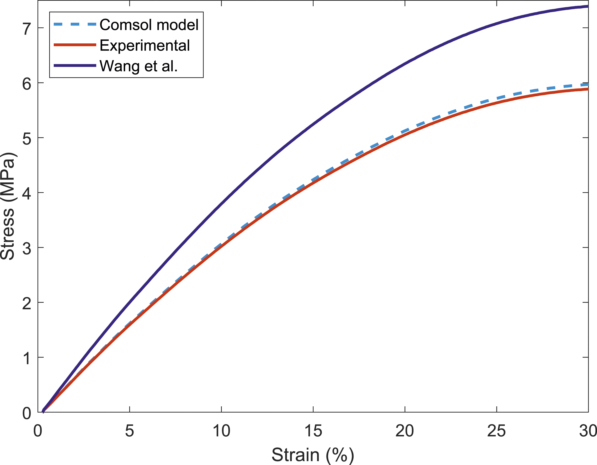
When the electrical properties of the material examined are investigated, there is a parallelism between their electrical and mechanical characteristics. When the length changes by
Finite element model
The finite element model of the strain sensor was developed using the COMSOL Multiphysics software. This software is a powerful engineering simulation software used to simulate the interactions of multiple physical domains. It allows the simultaneous analysis of various physical phenomena such as electromagnetism, mechanics, fluid dynamics, and heat transfer. For the finite element analysis, the 3D geometry of the sensor was first created using COMSOL software. The dimensions of the geometry were defined according to the design shown in Figure 1. Because both the mechanical and electrical components of the sensor were examined during the analysis process, the model was created using the AC/DC and structural mechanics modules of the software. The Ogden model was used to describe and analyze the mechanical behavior of the flexible substrate (TPU). The hyperelastic material model is used to describe the behavior of elastic materials. It is widely used to describe the stress-strain characteristics of materials and to model the behaviors of rubber and elastomer materials. After the model definition process, the physical properties of the TPU and liquid conductive silver materials to be used were transferred to the software. In the last stage of the analysis, the physical domain (boundary conditions) of the model was defined. To accurately express the physical structure of the strain sensor, a boundary condition was defined between the flexible conductive channels and liquid silver. According to this limitation, it is assumed that the volume of the channel changes as a result of the deformation of the sensor channel. Then, the necessary finite element analysis settings were defined, and the mesh was assigned to the model. By ensuring sufficient mesh resolution, the accuracy of the analysis results is increased. Finally, analyses were conducted using the mechanical and AC/DC modules to calculate the deformation of the sensor’s substrate and resistance values, respectively. The results were then examined.
Results and discussion
Model validation using experimental methods
The TPU material properties on the bottom substrate of the flexible strain sensor may vary depending on the printing parameters of the 3D printer. For this reason, it is necessary to compare the Ogden model results obtained by COMSOL with the experimental results. Thus, the experimental results can be verified using the simulation data. First, a strain sensor was fabricated by the FDM method using the 3D printing parameters listed in Table 1. Then, the stress-strain values of the sensor were obtained using the experimental setup shown in Figure 4. Stress-strain data measured both experimentally and with the COMSOL model are presented in Figure 5. To ensure the accuracy of the results, a comparison was made with the findings of Wang et al. 52
The strain output was in the range of 0%-30% as seen from the results. Tensile strength values were obtained experimentally, using the COMSOL model, and Wang et al. measured 5.912, 5.995, and 7.425 MPa MPa, respectively. After passing this point, the material broke. The elasticity modulus calculated as a result of the experimental study was approximately the same as that reported by the manufacturer. Figure 5 shows that the stress-strain values measured by the real-time sensor and the COMSOL model results were very close to each other. These results demonstrate the accuracy of the Ogden model. When the results of this study were compared with those of the study conducted by Wang et al., they were found to show similar trends. It is thought that the resulting deviation values arise from the 3D fabrication process. It is possible to fabricate TPU substrate materials with higher strength by changing the printing parameters.
The simulation results obtained using the finite element model were confirmed with experimental results. Both the electrical resistance-strain and force-displacement curves were calculated and plotted. For these results, the experimental setup shown in Figure 4 was used. A uniaxial force was gradually applied to the strain sensor with the device, up to a force of 50 N. The amount of extension was transferred to the computer by the displacement sensor on the device. The results of the force-displacement curve are presented in Figure 6(a). During testing, a near force of approximately 50 N was generated, and a maximum displacement of 34.95 mm was measured on the strain sensor. Comparison between simulation and experimental data for strain sensor (a) Force-displacement, (b) Strain-electrical resistance.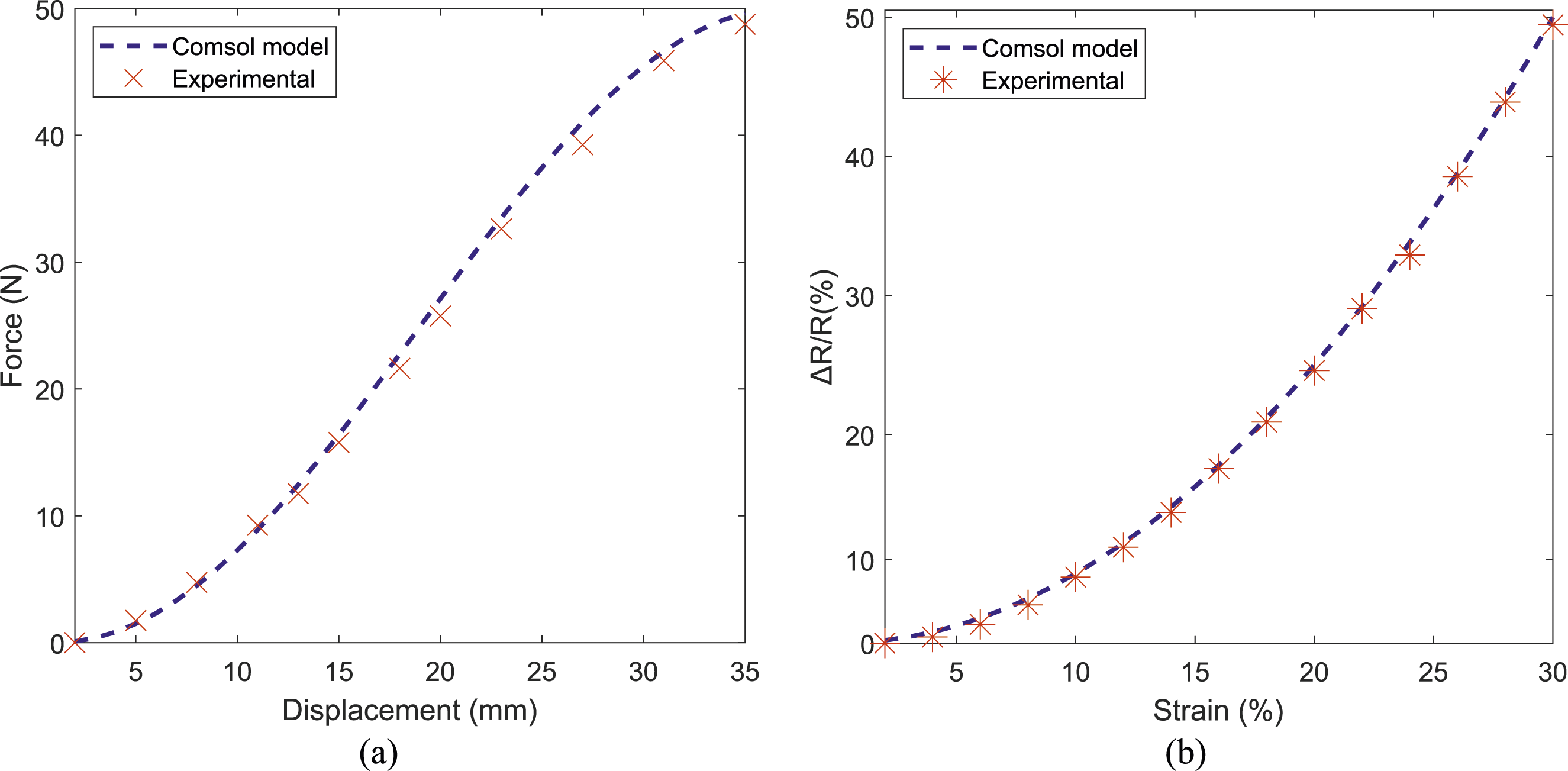
Depending on the applied force, the sensor elongates and a change in electrical resistance (ΔR) occurs. These changes were measured with the help of an established circuit and a multimeter. Then, strain (ε) was calculated by taking into account the elongation and initial lengths of the sensor. The results regarding the electrical resistance-strain curve are shown in Figure 6(b). Using these data, the gauge factor (GF) of the flexible strain sensor was calculated. Details about the calculation are given in Section experimental setup. The strain sensor sensitivity is based on GF. The higher the gauge factor, the more sensitive the strain sensor. When the resistance-strain curve is examined, it is seen that there is a close to linear relationship between the strain and the resistance change. The results showed little or no hysteresis. The change in electrical resistance at the maximum extension of the strain sensor was measured as %49.85. As a result, the gauge factor was calculated as 1.66. This value is acceptable for a sensor fabricated by AM. The GF value is affected by different aspects because it depends on resistance and strain. As the sensor was extended, changes in the initial electrical resistance occurred due to stress accumulation. In addition, stress accumulation also occurred in the TPU substrate, and the channels were deformed as a result of the high elongation in the sensor.
The data calculated using the Ogden model in COMSOL software were compared with the real-time measured data, as shown in Figure 6. There is a close linear relationship and harmony between the results. As a result, with the developed hyperelastic model, the displacement, resistance, and strain values of the strain sensor with non-linear behavior were calculated at a level close to the real values. The proposed model can predict the behavior of the sensor at high strain levels.
Resistance vs strain measurements
The resistance change of the flexible strain sensor was calculated using the electrical resistance and strain curves calculated from previous experimental studies. The resistance-strain curve is shown in Figure 7. The initial resistance of the sensor was approximately 180 Ω. As a result of the gradually applied force, the resistance value increased by approximately 30%, resulting in a resistance change of approximately 269.35 Ω. There is a linear relationship between the increase in the extension amount and the resistance value. Resistance-strain curve for strain sensor.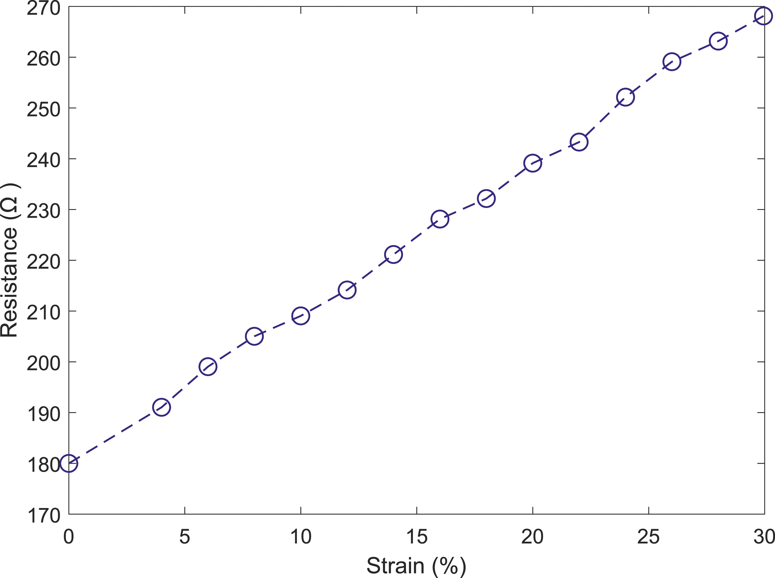
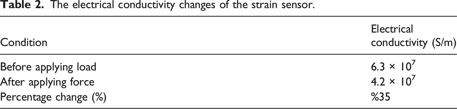
The electrical conductivity changes of the strain sensor.
Substrate thickness optimization
In addition to the electrical and mechanical properties, the effect of changing the geometric properties of the flexible strain sensor on its sensitivity was examined. For this purpose, the experimental process of strain sensors fabricated in different geometries were experimentally fabricated using the platform shown in Figure 4. The results of the effect of the TPU substrate thickness on the sensitivity of the flexible strain sensor are presented in Figure 8. In this graph, the concept of sensitivity is examined through an electrical resistance change. An increase in the sensitivity of the sensor was observed with decreasing TPU layer substrate thickness. At the 30% strain level, sensitivity increased by 9% when the sensor thickness decreased from 2 to 1.2 mm. As the TPU substrate thickness decreases, there will be an increase in the force transmitted to the channels; therefore, it is normal to observe an increase in the sensitivity of the sensor. As a result, the thinner the TPU substrate, the higher the sensitivity of the sensor to deformation. Effect of strain sensor thickness on sensitivity.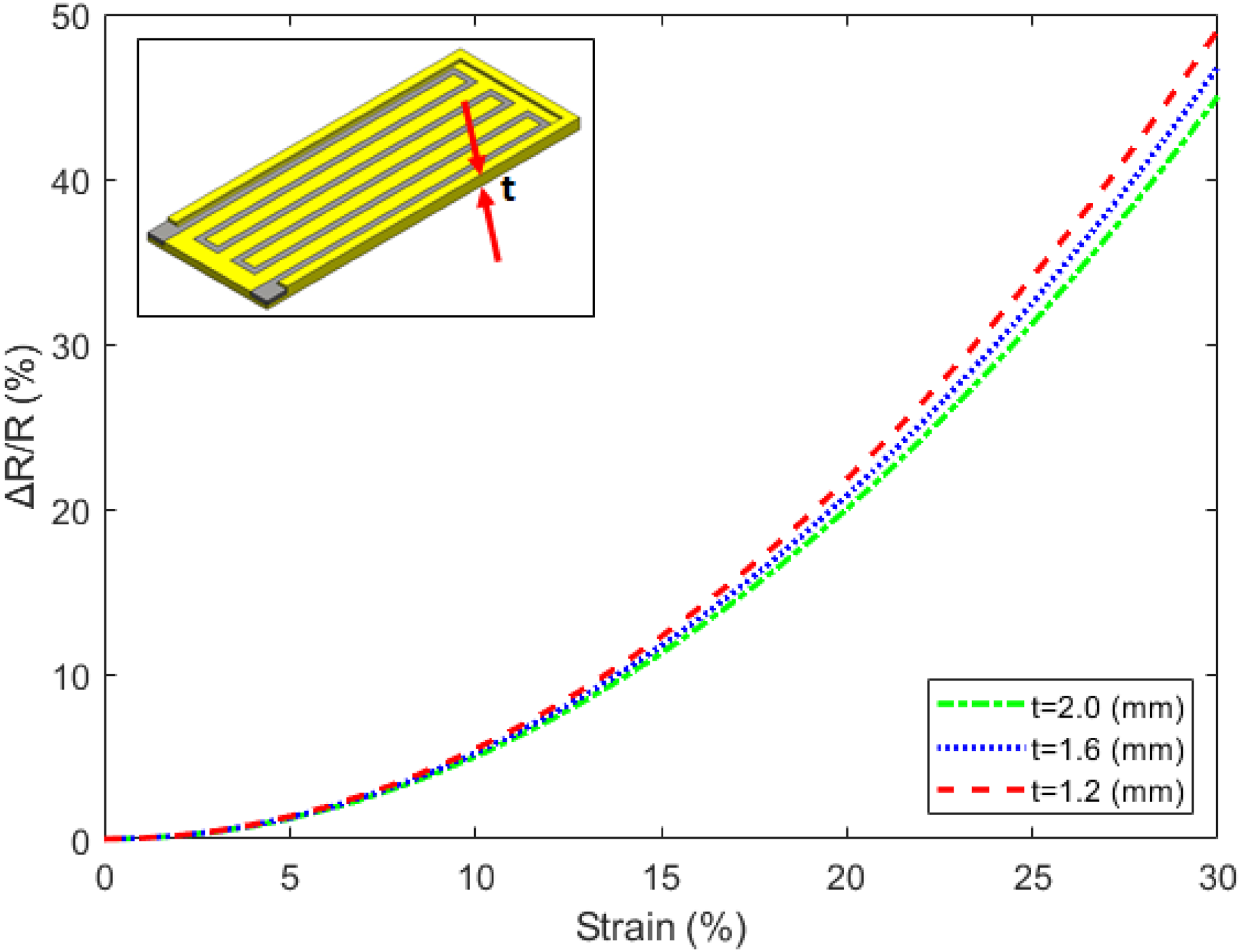
Discussion
Strain sensors have emerged as a tool for measuring and monitoring mechanical deformation with high precision and reliability in various engineering applications. In this study, the advances, difficulties, and potential future aspects of strain sensor technology were examined, and the flexible strain sensor fabricated by the FDM method was compared with resistance type sensors reported in the literature.53–60 Our results demonstrate that strain sensors are widely used in many industrial fields. In particular, strain sensors produced for fields such as structural health monitoring, medical devices, robotic systems, and smart materials, in which strain sensors play a critical role, will be applicable. However, current strain sensor technologies also have some limitations. Issues such as sensitivity, cost, sensitivity to temperature changes, and long-term stability can affect the performance of these sensors. In this context, future research should focus on overcoming these limitations and developing more advanced strain sensor technologies.
The mechanical mismatch between the flexible TPU matrix and the rigid silver conductive channel is a critical factor that could affect the integrity of the conductive pathway under mechanical stress. TPU is known for its elasticity and flexibility, whereas silver, being a metal, is significantly stiffer and less capable of withstanding deformation without breaking. When a load is applied, the TPU will undergo deformation due to its elastomeric nature. However, the silver channel, due to its comparatively brittle nature, may not deform in a similar manner. This difference in mechanical behavior can lead to the development of stress concentrations at the interface between the silver channel and the TPU matrix. If the applied load exceeds the adhesion strength or the deformation capacity of the silver, there is a possibility that the silver channel could crack, delaminate, or lose its contact with the TPU substrate. This phenomenon is particularly relevant in applications where the composite material is subject to repeated or significant mechanical stresses. The loss of contact between the silver channel and the TPU could result in a failure of the conductive pathway, leading to a degradation in the electrical performance of the material. To alleviate this problem, strategies such as surface treatment of TPU to improve silver adhesion or use of interlayers that can better accommodate mechanical incompatibility should be investigated. Additionally, the design of the silver pattern can be optimized to distribute stress more evenly, reducing the likelihood of failure. Future work could include experimental validation of these strategies and modeling efforts to predict the behavior of the composite under different loading conditions.
The conductive silver liquid used in this study is composed primarily of silver nanoparticles suspended in a solvent or resin. This composition provides the liquid with its high electrical conductivity, approximately 6.3 × 10⁷ S/m, which is a hallmark of silver. Upon curing, typically through heat or UV exposure, the silver particles form a continuous, conductive network, ensuring minimal resistivity. The cured silver layer offers excellent adhesion to various substrates and maintains flexibility, making it ideal for applications in flexible electronics. Additionally, the electrical properties of the cured silver layer are generally stable, though they can be affected by environmental factors such as humidity and oxidation over time.
In this study, experimental studies were conducted to improve the cost, sensitivity, and characterization features of strain sensors, taking into account their existing limitations. Although the sensor fabricated using 3D printing technology lags behind in performance optimization compared with other studies, it has shown the potential of FDM to compete with other techniques for small-scale sensor production. This technology significantly reduces material waste as it creates parts by adding material layer by layer. FDM also facilitates the production of parts with complex geometry and increases design freedom, because the internal structure or complex details of at part do not pose problems during manufacturing. For these reasons, AM has become an attractive, flexible and cost-effective manufacturing method that can adapt to the rapidly changing needs of the industry. Owing to these features, strain sensors have become popular using the AM method. The current study enabled the experimental process of the sensor to be examined in many aspects, providing a comprehensive characterization process as well as a manufacturing method. These results were verified by finite element analysis. According to studies conducted using the same fabrication technique, the sensor sensitivity was within the acceptable range. Various improvements can be made to improve the performance of additively manufactured strain sensors.
Looking to the future, the future of strain sensor technology holds great promise; together with evolving technologies such as artificial intelligence and machine learning, integration and further innovations are anticipated. These advances could enable the creation of autonomous systems capable of adaptive structure monitoring and predictive maintenance, thus heralding the beginning of a new era for smart infrastructure and smart manufacturing. As a result, strain sensors play an important role in modern engineering applications, providing a means to accurately measure and monitor structural deformation. Although significant advances have been made, there are challenges remain to be resolved, and ongoing research is required to unlock the full potential of strain sensor technology in a variety of fields – from aviation to healthcare. By overcoming these challenges and adopting emerging technologies, the power of strain sensors can be harnessed to create safer, more efficient, and more resilient systems for the benefit of society.
Conclusion
As a result of developments in additive manufacturing (AM) technology, the fabrication of small-scale strain sensors with complex designs has become possible. In this study, a resistive strain sensor, which is a transducer that detects mechanical deformation by measuring changes in electrical resistance, was examined. This sensor consists of the integration of a flexible substrate with a structure containing conductive channels. The full characterization of the flexible strain sensor is critical for determining both the mechanical and electrical properties. The present work presents the modeling, fabrication, and characterization processes for the development of a flexible strain sensor.
In this study, a prototype of a single-axis flexible strain sensor was fabricated using the molding technique. The flexible substrate of the sensor was fabricated using FDM, an AM method, with dimensions of 20 mm × 60 mm and a thickness of 2 mm. The liquid conductive silver was then injected into the mold channels. The electromechanical finite element model of the sensor was realized using COMSOL software and was used to validate the real-time experimental results. The characterization process was carried out by establishing experimental and numerical setups. When the model results were compared with the real-time characterization experiment results, the results were found to be in good agreement. Thus, the features of the resistive type strain sensor are better understood. Studies were conducted to maximize sensitivity by changing the geometric properties of the sensor. At the 30% strain level, sensitivity increased by 9% when the sensor thickness decreased from 2 to 1.2 mm. An increase in the sensitivity of the sensor was observed as the TPU substrate thickness decreased. As a result of the gradually applied force, the strain sensor showed a maximum displacement of 34.95 mm and resistance change of 269.35 Ω. To determine the sensor sensitivity, electrical resistance-strain curve was drawn, and the gauge factor was calculated. When this curve was examined, there was a close to linear relationship between the strain and resistance changes. The results showed little or no hysteresis. The change in electrical resistance at the maximum reach point of the strain sensor was measured as 49.85%. As a result, the indicator factor was calculated as 1.66. This value is acceptable for a sensor fabricated by the AM method. Tensile tests were also performed to investigate the effects of stress accumulation on the flexible base. The maximum tensile strength of the sensor was 5.912 MPa. The results of this study show that the strain sensor exhibits high linearity sensitivity and low hysteresis performance. It also provides design guidelines and roadmaps for sensors and demonstrates the potential of AM to create complex designs and sensor platforms for various applications.
Footnotes
Acknowledgments
The authors of this article would like to thank Assoc. Prof. Ishak Ertugrul, and Lecturer Burak Ergunes for their support.
Declaration of conflicting interests
The author(s) declared no potential conflicts of interest with respect to the research, authorship, and/or publication of this article.
Funding
The author(s) disclosed receipt of the following financial support for the research, authorship, and/or publication of this article: This work was supported by the Mus Alparslan University Technology Research and Project Coordination Unit as a project numbered BAP-23-TBMYO-4902-01.
Data availability statement
All data underlying the results are available as part of the article and no additional source data are required.