
Abstract
In this article, we have explored screen printing as a fast and reliable process for the deposition of nanocomposite layer on glass fiber-reinforced plastic (GFRP) substrate for in situ structural health monitoring. The screen-printed sensor comprised of a thermoplastic matrix (high density polystyrene) and a dispersed nanofiller (carbon nanoparticles). Notches of different sizes (2.5 mm and 4.0 mm) were introduced to study the response of sensors to an existing damage. Stress concentrations were plotted across the width and the sensor results were correlated with the simulated stress concentrations to evaluate the response of sensors with respect to local stress concentrations. It was found that the screen-printed sensors responded to the stress concentrations since the layers were deposited in the vicinity of notches. The gauge factors altered due to the presence of notches indicating sensor sensitivity to the preexisting damage and resultant stress concentrations.
Introduction
Composites have unique advantages over monolithic materials like high strength, low density, and better corrosion resistance. Due to these unique properties, there is an increasing trend of their use in the aerospace and aircraft industry. 1 The aircraft/spacecraft has to perform in a very cold/hot environment and the possibility of an in-service damage/crack in the aircraft/spacecraft’s structure is inevitable. This calls for a regime for continuous monitoring of these composites structural parts. 2,3 For the prevention of a catastrophic failure owing to further crack propagation, several different kinds of techniques (i.e. acoustic emission, infrared and ultrasonic, etc.) have been developed to analyze these cracks in the early stage. 3 The fabrication of composite piezoresistive sensors and their integration during composite fabrication is one of the most suitable and cost-effective technique for continuous online structural health monitoring of aircraft structures whereby the change in resistance could be correlated to the strain. 4 –15 The fabrication techniques are compatible with composite manufacturing processes and the sensitivities of these sensors could be tailored to achieve desired monitoring results. 4,5
In nanocomposites, a certain minimum concentration of conductive nanofillers is maintained to obtain the electrical conductivity. It goes without saying that below this threshold, conductivity can’t be achieved as conductive particles don’t form “percolation networks.” The percolation threshold is defined as the specific concentration of the conductive fillers that is needed to overcome the insulator barrier and creating the path for the flow of electrons to obtain electrical conductivity. “Quantum tunneling effect” is the phenomenon through which the electrons hop from one charged particle to another in the percolation networks. 16
According to the classical theory of quantum mechanics, when an electron wave faces the insulator barrier, it reflects back and cannot pass through it, but the latest research of quantum mechanics reveals that there is a chance of surmounting the barrier and this happens because of the dual nature of subatomic particles. The Heisenberg uncertainty principle also states that the probability of an electron to hop across the potential barrier is greater than “0.” So the electron can still hop across a barrier when its kinetic energy is less than the potential of this barrier the electron is said to have tunneled through the barrier. 17
Once the sensitive conductive coating is prepared, the next step is to implant this coating on composite samples. Various different techniques have been used in different research works for this purpose, that is, hand layup, molding technique, microcontact printing, inkjet printing, and so on. 18 –23 These techniques, though not without advantages, have certain difficulties associated with them such as high cost, nonuniformity, complexity of the process, and slow processing.
Screen printing is utilized in the present research work to achieve the homogeneous thickness of implanted coating on composites. This technique is not only used widely in textile industry to print patterns on the textile fabrics but is also employed for wearable sensing patterns and flexible electronics. 24,25 Screen printing is user-friendly, efficient in outcome, economic, amenable to high volume production, and reproducible. 26 Several kinds of mesh sizes are used commercially for different materials. Generally, 150 M mesh size is used for fabrics, 250 M mesh size is used for plastics and composites, and 350 M mesh size is used for visiting cards and glass products. Mesh size “M” is considered as “the number of holes per square inch.” Since screen printing can be employed on any substrate after necessary surface preparation techniques have been applied, if necessary, the thermoplastic composites which are manufactured at high temperature can be used as substrates once the polymer matrix is in frozen state back from its high-temperature molten state.
The composite specimens for the deposition of sensing layers can be prepared using various composite’s manufacturing processes. The selection of a particular manufacturing process depends on a host of factors. Some of the more important factors or performance criteria have been enlisted in Table 1. 27 Most common composite’s fabrication processes have been compared on a scale of 1 to 5 with 5 being the highest value of the performance criterion.
Comparison of principle composite’s manufacturing techniques.
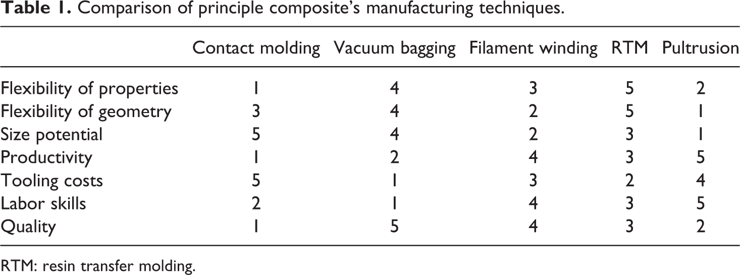
RTM: resin transfer molding.
It can be inferred from Table 1 that vacuum bagging is the most versatile and cost-effective technique for manufacturing of composites. Even though its productivity is lower as compared to other techniques, in laboratory settings, this particular drawback does not hamper its adoption for specimen preparation. Therefore a variant of this technique known as vacuum-assisted resin transfer molding (VARTM) was adopted for manufacturing composite specimens to serve as substrates for the screen printing of nanocomposite strain sensors.
The aim of the present research work is the fabrication of strain sensors by commercially available traditional screen printing on laminated composite specimens and to determine the sensors’ sensitivity in terms of their gauge factor (G) in case of an induced damage. The stress–strain response as well as the stress concentrations around the notches in composite specimens will be correlated with the sensors normalized resistance (dR/R) and strain (ε) as it is indicated in equation (1). A finite element-based numerical simulation will be used to determine the stress concentrations around the notches
Materials and methods
Preparation of smart sensing layer
High density polystyrene (PS) was selected as the matrix material whereas carbon nanoparticles (CNPs) supplied by Degussa (Germany) were used as nanoparticles. These particles have spherical geometry.
It has been found through repeated and systematic investigations that when weight concentration of these particles is maintained at 35%, the resulting polymer matrix composite becomes piezoresistive 4,28,29 since the said concentration pertains to the percolation threshold of these nanoparticles in the PS.
Firstly, beads of PS are placed on a laboratory scale vacuum oven to remove moisture and after that they are weighed on laboratory scale microbalance having the precision of 0.01 mg. The concentration of CNPs (provided by Degussa) depends upon the total weight of PS beads. CNPs are weighed 35% of PS in a small beaker on a microbalance. Nitrobenzene is taken as 7 ml/g of total weight of CNPs and PS. CNPs and nitrobenzene is mixed together with the help of mechanical stirring on a hot plate for 2 h. The PS beads are added in the solution and the temperature is maintained at 70°C along with mechanical stirring. After an hour, heating is stopped as the PS is completely dispersed in the solution. For homogeneous solution, mechanical stirring is continued for 24 h. As a last step, the solution is placed in a sonicator for 2 h to achieve uniform dispersion of three elements. From first to last step, all the procedures are performed at ambient environmental conditions.
Particle size analysis results are shown in Figure 1.
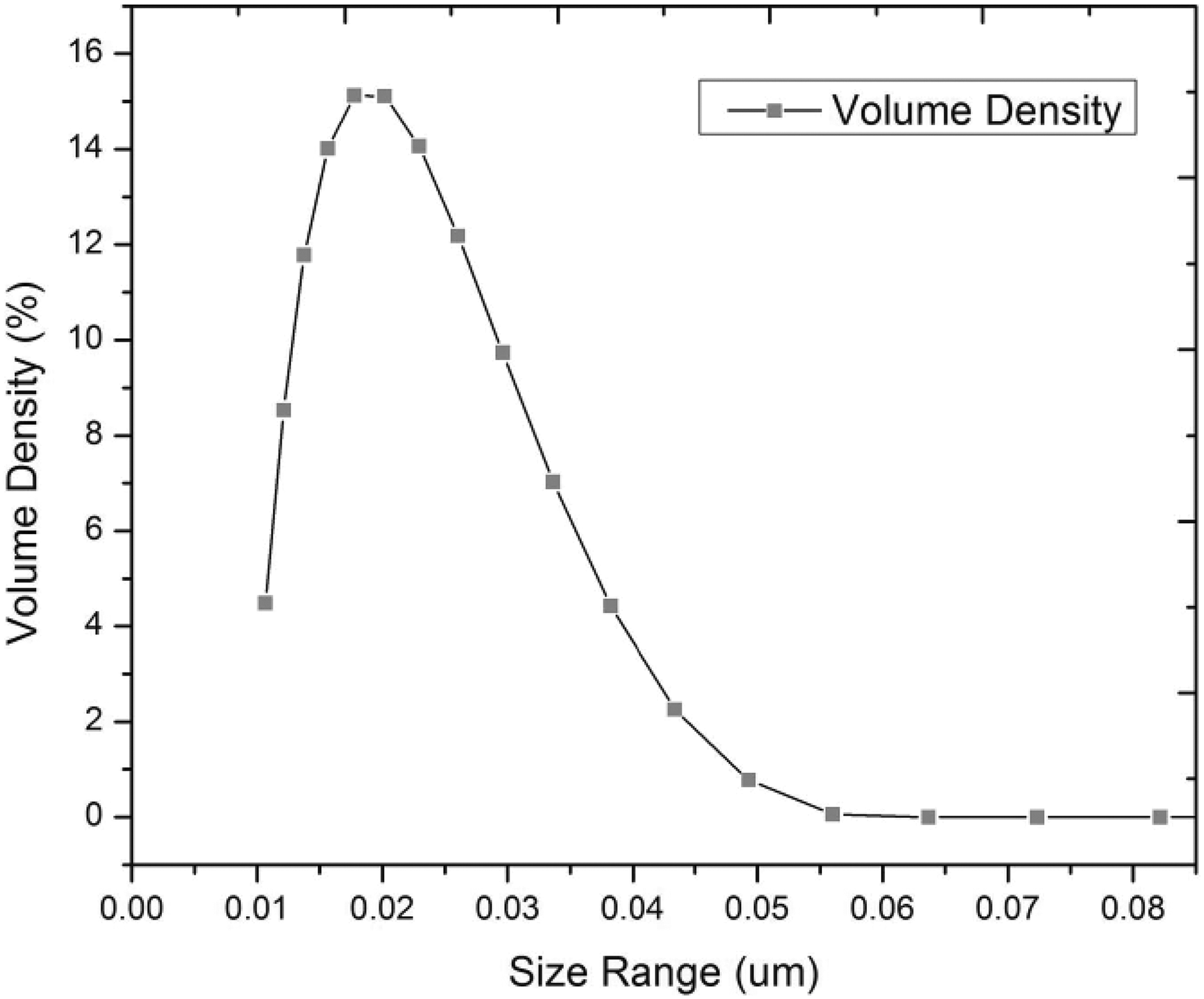
Particle size analysis of CNPs.
This graph clearly depicts particle size range of CNPs. The overall percentage volume density for CNPs varies from the sizes of 10–58 nm. The data display that peak volume density of particles lies in the range between 18 nm and 25 nm. Later on, same particles were characterized using MIRA3 TESCAN (Czech Republic) scanning electron microscope (SEM). The image obtained from SEM supports the particle size analysis as the average size of the particle varies between 20 nm and 38 nm as presented in Figure 2.
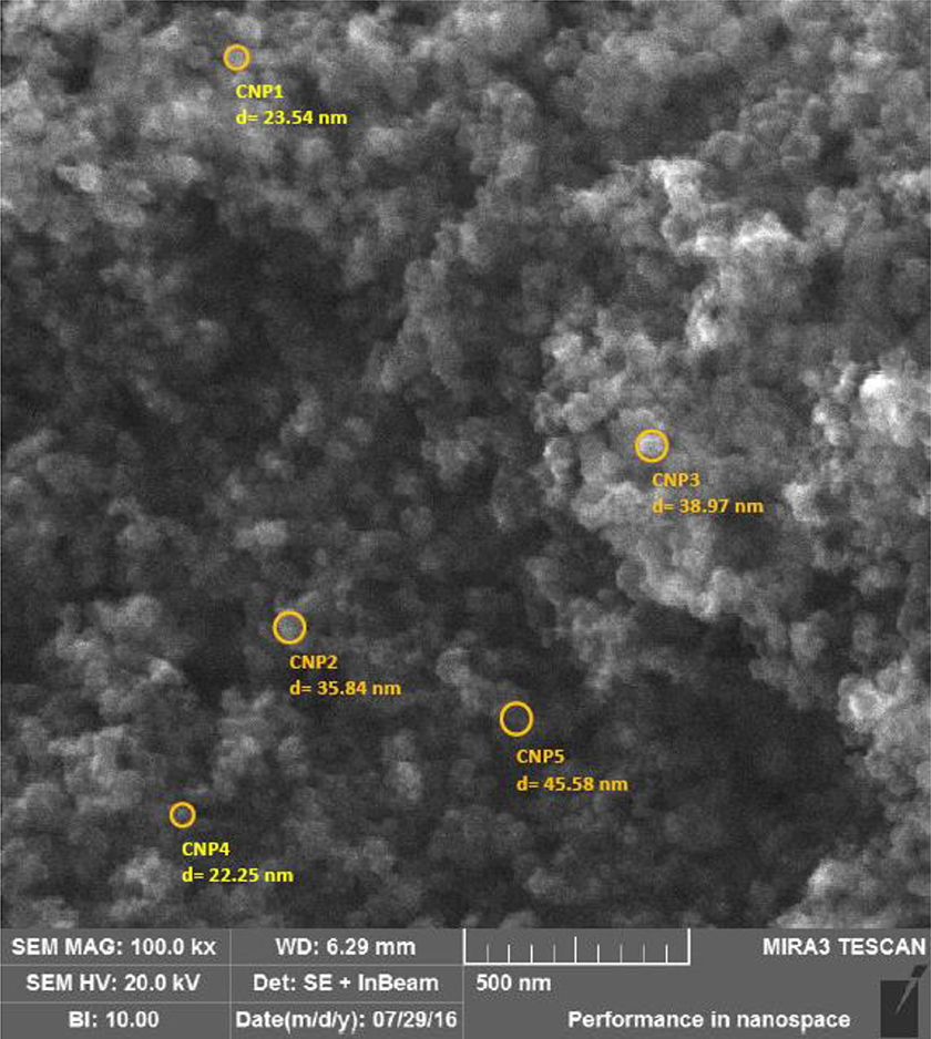
Image of CNPs obtained from SEM.
Fabrication of composite specimens
For composites fabrication, Interglas 92125 plain woven glass fiber reinforcement provided by Swiss Composites (Switzerland) is used. For matrix, epoxy resin Araldite LY5052 is used along with hardener Aradur 5052 provided by HUNTSMAN (USA). Eight plies of Interglas 92125 are placed in cross-ply configuration to form a symmetric laminate; [0/90/0/90]s. VARTM is employed for manufacturing the laminated composites, whose schematic diagram is displayed in Figure 3.
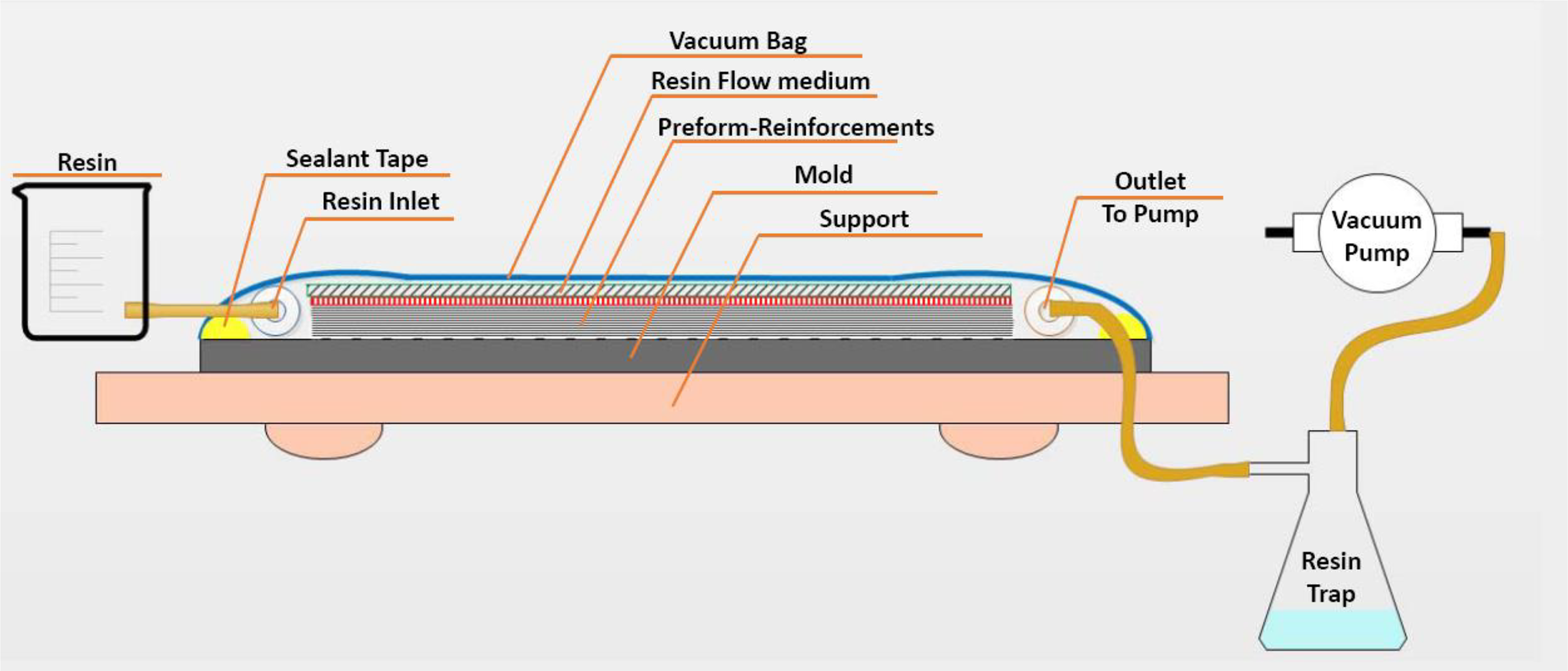
Schematic of VARTM setup.
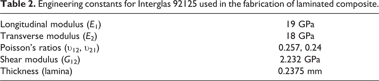
The basic properties of the laminate are highlighted in Table 2.
Engineering constants for Interglas 92125 used in the fabrication of laminated composite.
Specimen geometry
After the post curing step, laminated composite sheet was removed and cut into eight specimens, each of 25 cm × 2.5 cm × 1.9 mm dimensions, with the help of Metacut apparatus supplied by Metkon industries (Turkey). To prepare notched specimens, two holes each of 2.5 mm diameter were drilled in the middle of four specimens. Remaining specimens were drilled in the similar fashion but with notch diameter of 4 mm each. The dimensions and notch configurations for the two types of specimens are given in Figure 4.
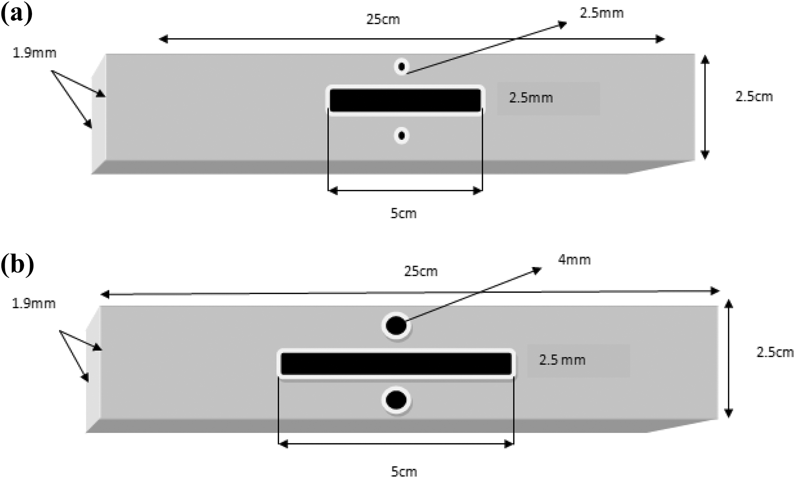
Dimensions and notch configurations for the two types of specimens: (a) notch diameter: 2.5 mm and (b) notch diameter: 4.0 mm.
Screen printing process
To carry out screen printing for depositing sensing pattern on the composites, the glass fiber-reinforced plastic (GFRP) composite specimen is placed below the screen and conductive ink is poured from a beaker onto the screen. With the help of a squeegee, ink is spread on the screen resulting in the conductive ink passing through the given pattern and forming a homogeneous layer of ink coated on the substrate. The deposited layer is then dried with the help of a handheld hot air blower. The procedure is repeated two more times to get the required thickness and initial resistance of the deposited sensing pattern. The viscosity of the conductive ink and the filler concentrations also play a role in determining the layer thickness deposited on the substrate. For the purpose of depositing the sensing pattern for structural health monitoring, a rectangular pattern of 5 × 0.5 cm2 was deposited. The three layers deposited on top of one another were left to air dry for 24 h before the specimens were mechanically tested. The screen used for the process along with the schematics of the process and the specimen are shown in Figure 5(a) and (b).
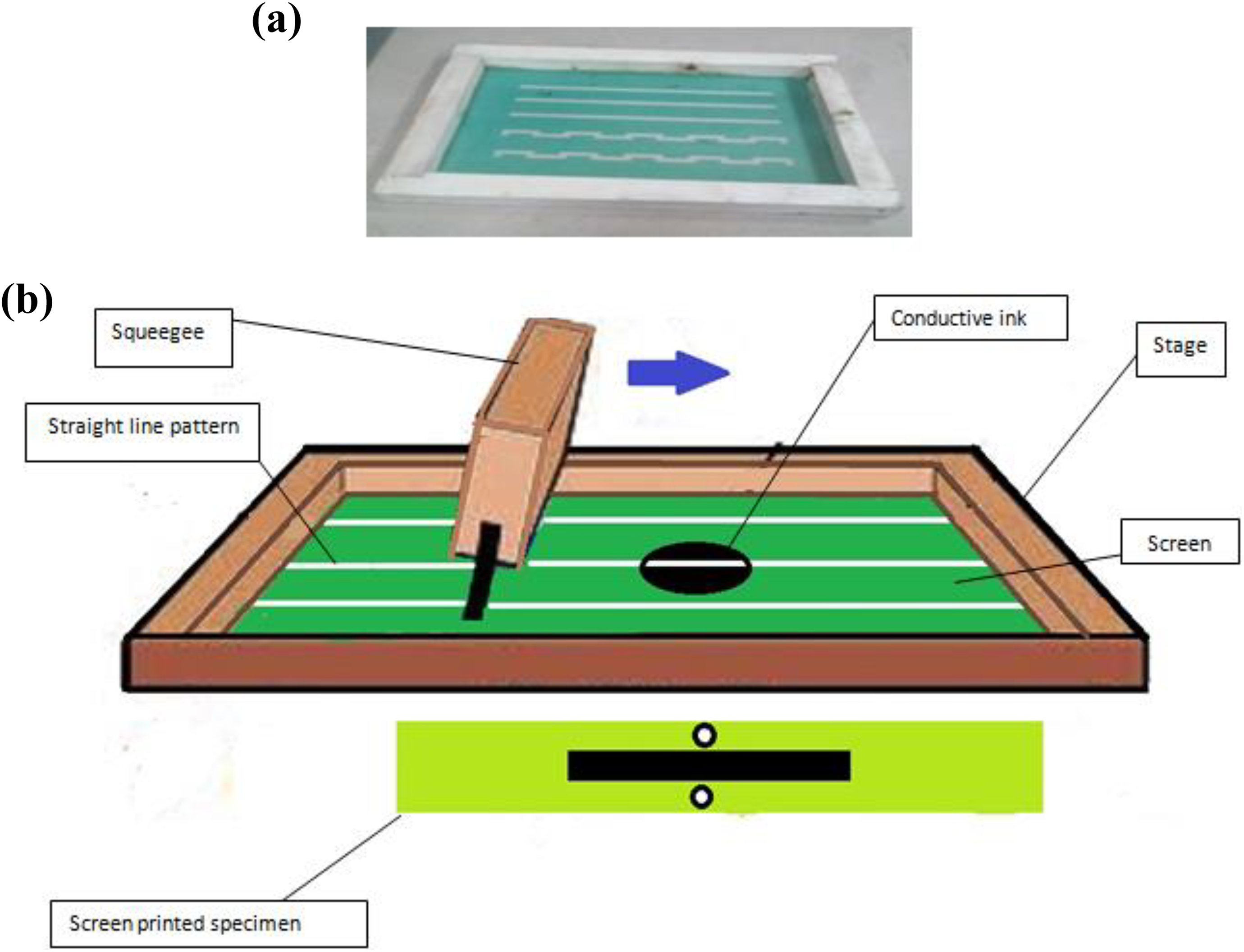
(a) Screen and (b) schematic of screen printing process.
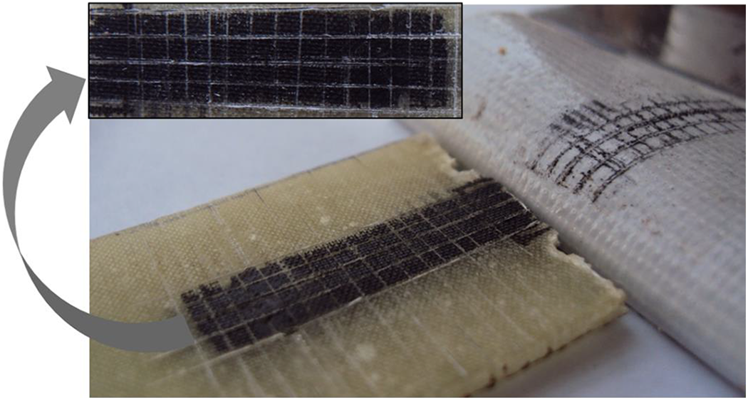
Cross hatch test as described in ASTM standard D2197-16, test method B was adopted to characterize the adhesive strength of the applied screen-printed coating on the laminated composite substrate. To prepare the screen-printed coated surface for the test, it was thoroughly cleaned, dewaxed, and degreased. A sharp blade was used to make cuts both horizontally and vertically to obtain a mesh with each mesh box having a size of 1 × 1 mm2. The cuts made were deep enough to reach the substrate. A pressure-sensitive adhesive tape was applied on the scribed area. The tape was scraped with an eraser to make sure that it tightly adheres with the coated surface and there is no air trapped within. The tape was then pulled off at 180° back over itself and the surface was observed for any indications of debonding of the coating from the surface. Adhesion was assessed on a scale of 0 to 5. A total of five samples were tested in this way. It was observed that small flakes of the coating detached at the intersections of the cuts. A total crosscut area not greater than 5% was affected. The observations correspond to ISO class 1 or ASTM class 4B according to the classification of cross hatch test results. The adhesive strength corresponding to this class is generally satisfactory for most structural applications.
Data acquisition and noise reduction
Commercially available data acquisition module, Keithley KUSB 3100 was used for the purpose of data acquisition. For data amplification, an instrumentation amplifier INA101 was employed. The schematic of the data acquisition module is depicted in Figure 6. In this system, the unknown resistance of the smart sensing layer was connected in Wheatstone configuration shown as R-sensor in Figure 7. Moreover, low-pass filters also helped reduce noise in the sensor output.
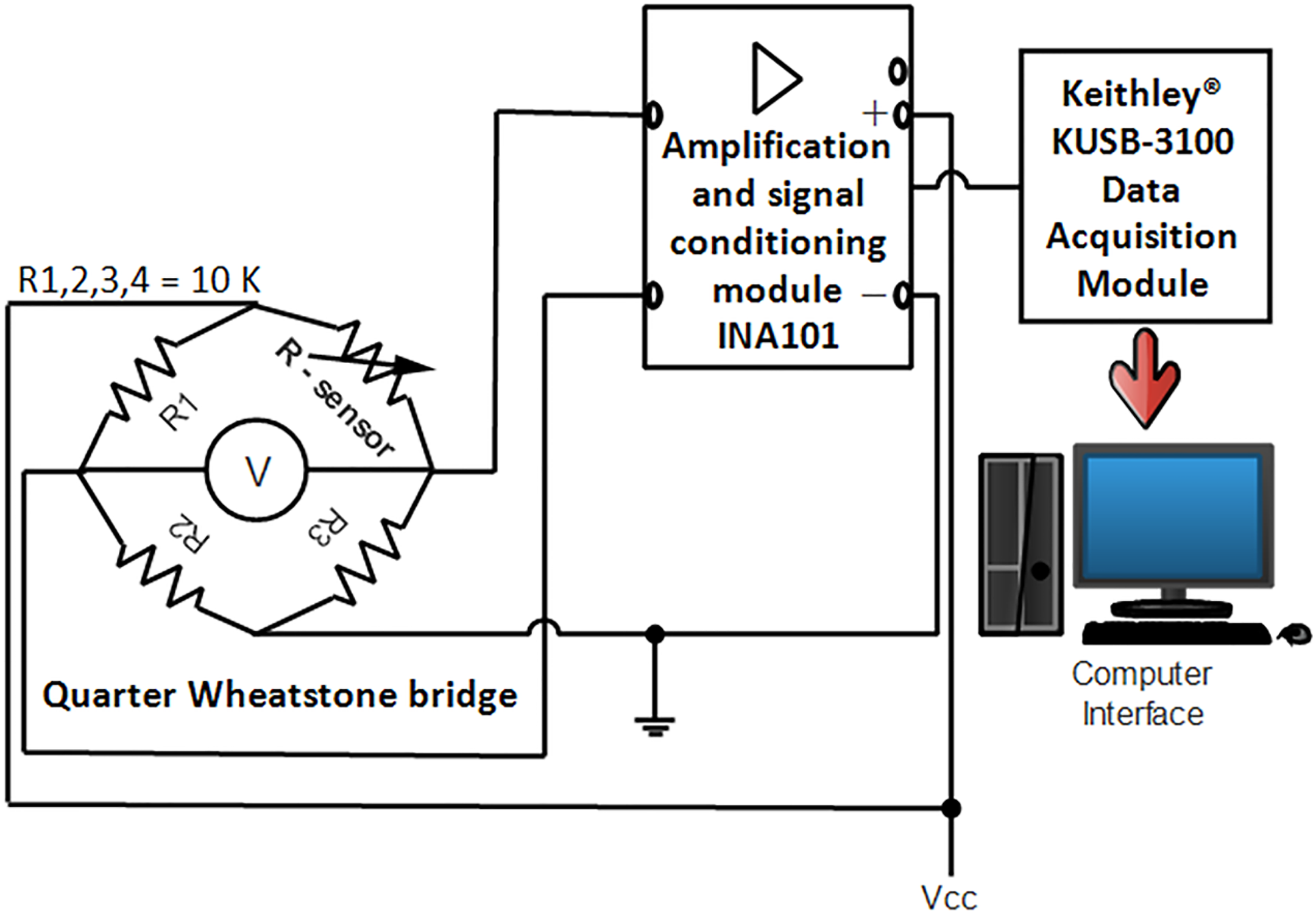
Schematic diagram of data acquisition system employed for data acquisition, linearization, and amplification.
Cross hatch testing of screen-printed specimen according to ASTM standard D2197-16, test method B.
Specimen connections with the data acquisition module
The screen-printed sensing layer was attached to thin and flexible copper wires with the help of silver conductive paint (supplied by RS paints, RS Components, UK) to minimize contact resistance (Figure 8). The two wires were meant to connect the screen-printed sensing layer in Wheatstone bridge configuration to the data acquisition and linearization module. In this way, the sensing layer resistance served as the unknown resistance in the Wheatstone bridge, whereas all the other three resistors in the bridge were fixed resistors meant for bridge balancing.
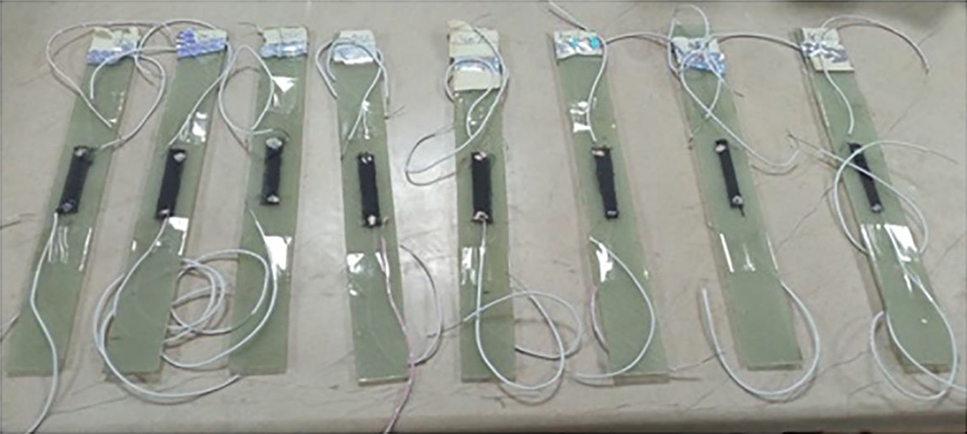
GFRP specimens with screen-printed sensing layer and wire connections at the extremities of the sensor.
Experimental methodology
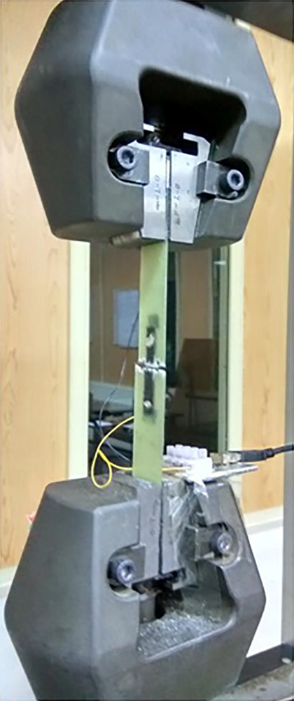
The two types of specimens (notch diameters of 2.5 and 4.0 mm) were tested on universal testing machine (UTM) at constant crosshead speed of 1 mm/min. The purpose of introducing two different diameters of notches was to be able to evaluate the sensor’s ability to monitor stress state in its vicinity which is a fundamental property required for a sensing mechanism in any structural health monitoring system.
A stress–strain plot along with the response of the screen-printed sensor for GFRP specimen drilled with 2.5 mm diameter notch is presented in Figure 9.
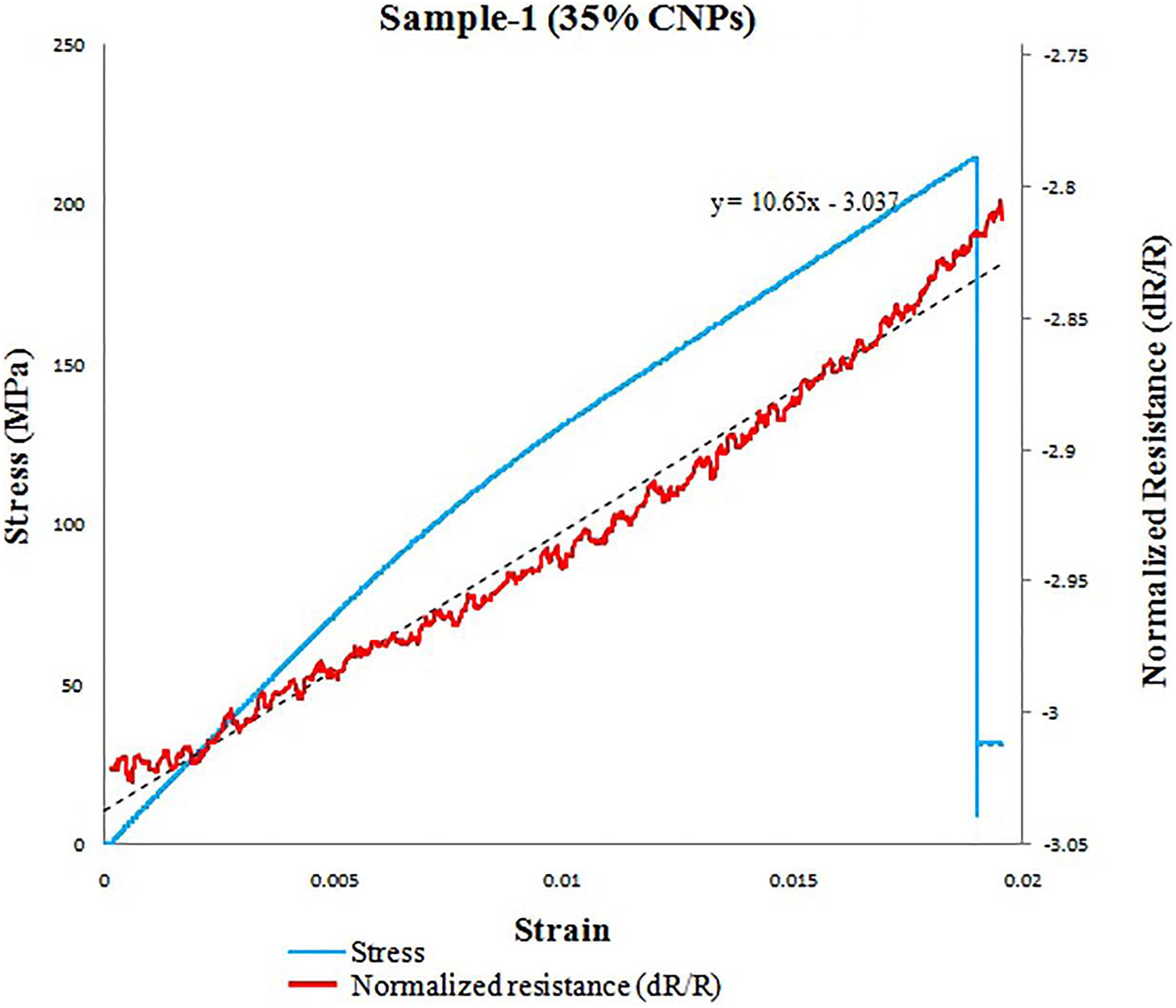
Stress–strain-normalized resistance plot for GFRP specimen having notch size of 2.5 mm.
It can be seen that the response of the sensor is largely linear with a gauge factor (G) of approximately 10.65 which is much higher than the traditional metal foil strain gauges. The notches resulted in stress concentrations around them and ultimately complete fracture in that region as shown in Figure 10.
Fractured GFRP specimen after the tensile test loaded on UTM.
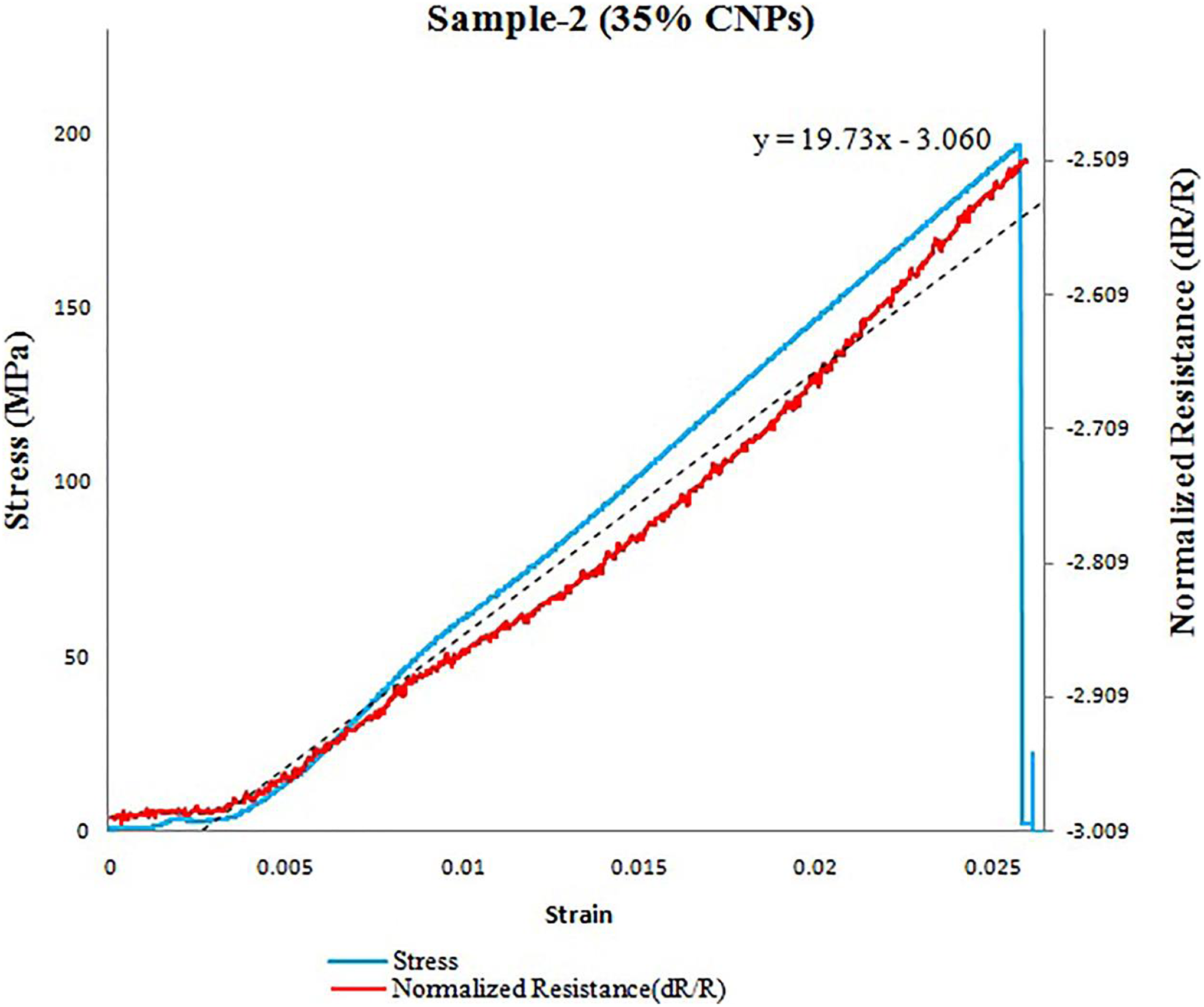
Similarly, the other group of specimens having notch size of 4 mm diameter were also tested on UTM in tensile test configuration. A representative plot is shown in Figure 11.
Stress–strain-normalized resistance plot for GFRP specimen having notch size of 4.0 mm.
The stress concentrations caused by 4.0 mm diameter notches in the middle of the specimens caused them to fail at lower global stress as compared to the 2.5 mm diameter notched specimens. The sensor response in the form of normalized resistance plot follows the stress–strain curve until final failure of the specimen. The response is largely linear here as well with a still higher gauge factor of approximately 19.7.
Results and discussion
To understand the stress distributions to correlate them to the sensor response, a model was developed for finite element analysis (FEA) using the commercially available code; ANSYS APDL. The basic mechanical parameters given in Table 1 were used to create a two-dimensional model.
Shell elements (four-node SHELL181) were employed for meshing the geometry. These four-node SHELL elements are a suitable choice to run this analysis because of their computational efficiency and suitability for the analysis of laminated composites.
The first analysis consisted of notched specimens having holes of 2.5 mm diameter made in the middle of the specimen.
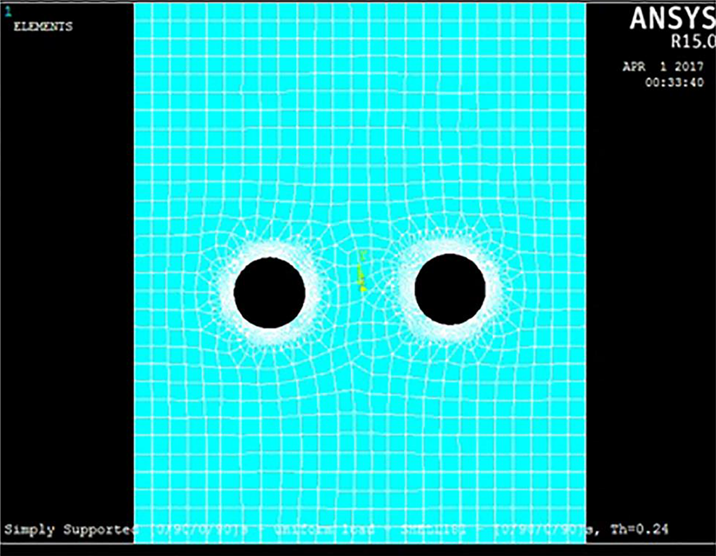
To perform FEA, the sample is clamped at one end (all Degrees of Freedom (DOF) = 0) and at the other end a load of 9260 N—the maximum load registered during tensile tests—is applied. The load is stepped in 100 equal steps. Free meshing feature of the ANSYS APDL was used to discretize the problem domain into a fine mesh. The stress distributions are expected to vary along the notches, therefore a still finer mesh having five times the nominal mesh density was applied along the notch perimeter. This resulted in 26,500 elements generated as depicted in Figure 12.
Meshed area around notches of 2.5 mm diameter in the tensile specimen.
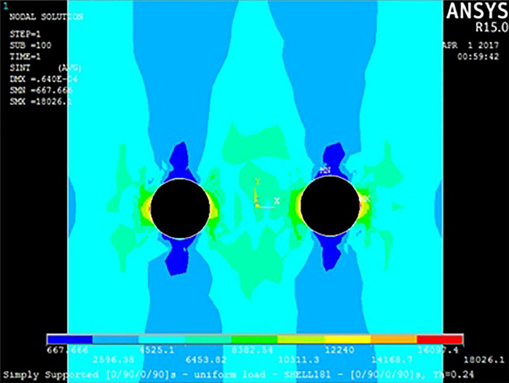
A contour plot of stress distributions around the notched area is shown in Figure 13. The stress concentrations are maximum around the notches and are minimum away from them.
Contour plot of stress distributions in the area around notches of 2.5 mm diameter in the tensile specimen.
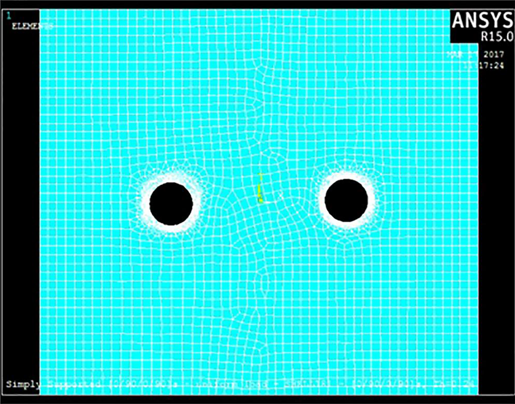
Another FEA model of tensile specimens having notches of diameter 4 mm drilled in the center was created in ANSYS APDL. Similar boundary conditions were used for these specimens with one end clamped and the other one was applied with 8886 N load. The load value was obtained from the experimental results. Free meshing scheme was employed for discretization of the problem domain. Higher mesh density was achieved around the perimeter of the notches through the application of mesh refinement algorithms as it is shown in Figure 14. A total number of 9334 elements were generated.
Meshed area around notches of 4 mm diameter in the tensile specimen.
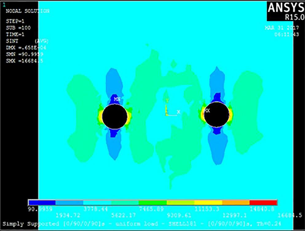
A contour plot of stress distributions around the notches of 4 mm diameter are shown in Figure 15. The stress concentrations are maximum around the notches and are minimum away from them.
Contour plot of stress distributions in the area around notches of 4 mm diameter in the tensile specimen.
These plots are divided into three sections: AB, BC, and CD. The AB section in the plot shows the stress intensity from specimen edge to the notch edge. The BC section gives stress intensity in the area between the two notches, from edge of one notch to another. The CD section gives the stress intensity from the farther edge of the second notch to the specimen edge. This is shown schematically in Figure 16.

Schematic illustration of notched tensile specimen with the three sections AB, BC, and CD it is divided into for the purpose of the analysis of stress distributions.
The plots given in Figures 17 and 18 give the distribution of stress intensity from one edge of the specimen to the other along its width (for both types of specimens). The stress intensity is minimum at point A and reaches the maximum value at point B which coincides with the notch edge. In the region between the notches, the stress intensity varies from a maximum at the notch edge, reduces to its nominal value in the middle of the two notches, and again rises to its maximum at the notch edge. Similarly in the region CD, the stress intensity gradually falls from a maximum value at the notch edge coinciding with point C to the nominal value at the specimen edge coinciding with point D.
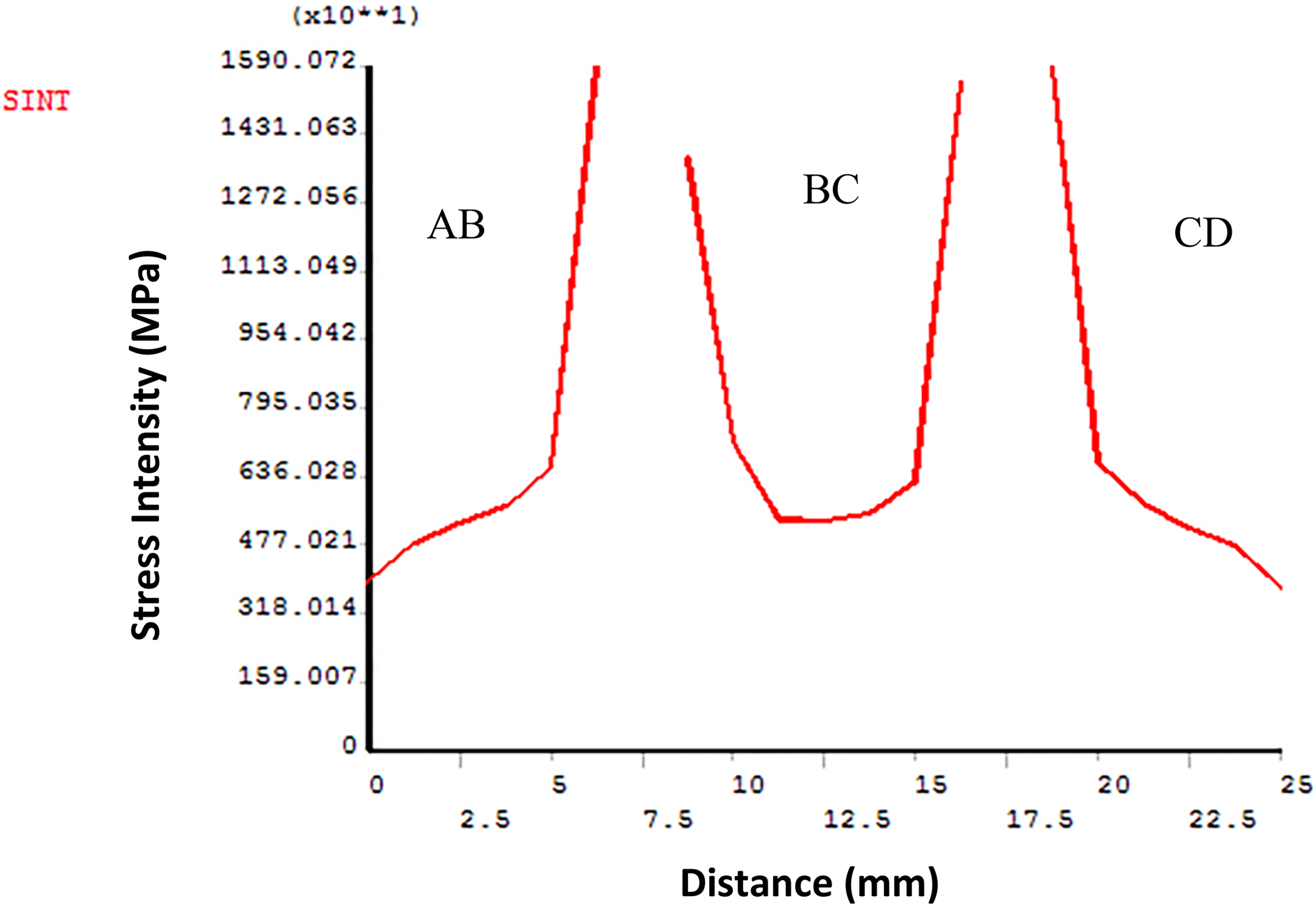
Stress intensity mapping along the width of specimens, notch size: 2.5 mm.
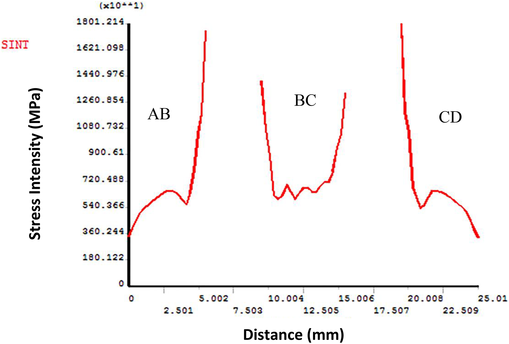
Stress intensity mapping along the width of specimens, notch size: 4.0 mm.
Conclusions
Since the matrix used in the screen-printed substrate is PS, the degradation temperature is relatively low. It was found that the degradation starts at 300°C in nitrogen environment. The service temperatures can be increased by using high-temperature-resistant thermoplastics as the matrix material.
The presence of notches alters the state of stress in its vicinity and increases the tendency for brittle fracture. This is due to four factors: generation of high local stresses, generating a triaxial stress state at the notch edge, causing high local strain hardening, and by increasing local strain rates. The screen-printed sensing layers printed in between the notches in both the cases are influenced by the local state of stresses due to the presence of notches and their size. This has led to drastically different gauge factors (sensitivities) for the two groups of specimens. These values are approximately 10 for a notch size of 2.5 mm and approximately 19 for a notch size of 4 mm. This is another advantage of screen-printed sensors as against the extraneously integrated traditional sensors, whereby the screen-printed sensors intimately follow the substrate response to the applied loads and local stress states due to the presence of material discontinuities. It is therefore concluded that the screen-printed sensor response is dependent on the state of stress at its boundaries as is evident from the conducted results and mapped stress concentrations along the width of the specimens. This has been done to ascertain the sensor response against the simulated damage in the form of induced notches of different diameters. This also validates the utility and application of these sensors for an integrated, online and in situ “structural health monitoring” system for composite structural parts.
Further study of the large strain-sensing ability of the smart sensing layer is focused at increasing the bandwidth of the dynamic response, minimization or correction of resistance drift, and determination of the long-term reliability of the sensor material.