
Abstract
The aim of the work was to verify the influence of positive pulses in the high-power impulse magnetron sputtering (HiPIMS) method on the formation of the adhesion interface between the Ti coating and the polyetheretherketone (PEEK). Two variants of PEEK materials were tested, a non-conductive one in the basic state and a conductive one filled with carbon nanotubes. The depth profile of the chemical composition was tested using the XPS method with Ar + ion bombardment. A positive pulse applied to the non-conductive PEEK enables the implantation of Ti ions, but the depth of implantation is lower than for a combination of a positive pulse with a DC negative bias applied to the conductive PEEK. However, a positive pulse has a clear effect on the formation of a chemically pure interface without the formation of an atomic inter-mixed layer.
Introduction
The application of metal coatings on polymers is limited in many technologies due to their electrical non-conductivity. In the case of magnetron sputtering, it is not possible to simply apply a negative bias to the non-conductive material to enhance the ion bombardment. One of the few ways to accelerate ions onto a non-conductive material is to use a radio frequency (RF) power supply or using a combination with plasma immersion ion implantation & deposition (PIII&D). 1 For conventional magnetron sputtering on non-conductive materials, the positive ions are accelerated onto the surface only by the voltage given by the difference between the plasma potential and the floating potential created on the non-conductive surface. The formation of the metal-polymer interface with the subsequent growth of the metal coating cannot then be improved by surface ion implantation enabling controlled coating growth.
One of the promising ways to coat non-conductive materials is by the HiPIMS (high-power impulse magnetron sputtering) method with a positive pulse.2,3 This method was introduced relatively recently, but the effect of a positive pulse in direct current (DC) pulsed magnetron sputtering has been known for some time.4–6 The standard HiPIMS method is based on the application of high power in short (tens µs) negative voltage pulses on magnetron cathodes. For the HiPIMS method with a positive pulse, a negative pulse is followed by a positive pulse that repels and accelerates positive ions from the space in front of the target toward the surface of the growing coating. Then, the ions can be accelerated to non-conductive materials such as polymers. 7
Another way to improve the adhesion of metal coatings to polymers is to use conductive polymers in combination with the HiPIMS method. It is possible to apply a negative bias to conductive polymers, which will accelerate the positive ions. In combination with a positive pulse, this effect can be further amplified. The mentioned methods are based on the principle that the coating grows atom by atom and copies the surface of the coated polymer. The thickness of these coatings is usually on the order of micrometres. For much larger coating thicknesses, methods where the input material is metal powder are more suitable. For example, cold spray technology is very promising. 8
Polyetheretherketone (PEEK) is a perspective polymer for coating applications. PEEK is electrically non-conductive, but if it contains carbon fibre (CF-PEEK) based fillers or carbon nanotube (CNT-PEEK) based fillers, its electrical resistivity approaches the level of conductive materials. As the electrical resistivity of the carbon PEEK composites decreases with increasing temperature, 9 the electrical conductivity can be also increased by deposition at higher temperatures. At the same time, higher temperatures can affect the diffusion of metal atoms 10 and partially promote the implantation process of metal ions.
PEEK polymers and their composites are increasingly used in applications where a replacement is required for standard metal materials. They are used where, for example, a low weight and, at the same time, higher temperature resistance are required. PEEK itself has a maximum long-term service temperature of 260°C and a short-term service temperature of 300°C. The coating may, for example, reduce the abrasion of the polymer surface, be used as an electrode on conductive polymers, or change the surface properties of polymer implants. 11 In all of these cases, the surface treatment is ensured by applying a metal coating, which must have a very good adhesion. 12
The aim of the work was to verify the influence of positive pulses on the formation of the Ti-PEEK interface, which can have a fundamental effect on the adhesion. The analyses focused on the evaluation of the depth of the implanted Ti ions and, at the same time, on the chemical composition of the Ti-PEEK interface. As a base material, two PEEK materials were used. The first PEEK material was used to test in the basic state, which is non-conductive. The second PEEK material filled with carbon nanotubes had higher conductivity, and was used to verify the effect of the DC bias.
Materials and methods
Materials
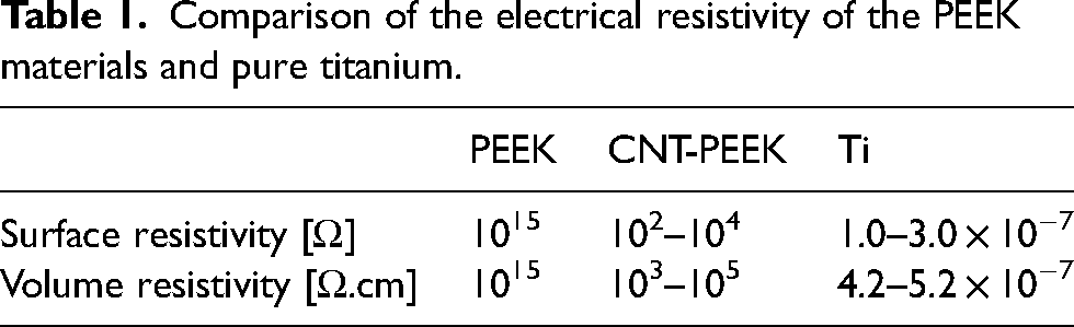
Two PEEK materials with different electrical resistivity ρ (respectively conductance σ = 1/ρ) were selected for testing. PEEK (TECAPEEK natural) with high electrical resistivity and CNT-PEEK (TECAPEEK ELS nano black) with lower electrical resistivity, which was reduced by a carbon nanotube filler. Both materials were obtained from the producer Ensinger GmbH, Germany. Table 1 shows the surface and volume resistivity of the PEEK materials according to the data from the manufacturer's material sheets. For comparison, Table 1 shows data for pure titanium, where the surface electrical resistance corresponds to a thin film deposited with magnetron sputtering in a thickness range of 5–80 nm 13 and the volume electrical resistance corresponds to the tabular values for bulk titanium.
Comparison of the electrical resistivity of the PEEK materials and pure titanium.
The PEEK samples d 20 × 3 mm were cut from bars, which were standardly produced by injection moulding of a Victrex® PEEK input material. The sample surfaces were metallographically ground with sandpapers with grits from P600 to P2000 and polished to a mirror finish using a Buehler MasterPrep Alumina with finely dispersed aluminum oxide of 0.05 µm nominal abrasive size in a basic (pH∼10.5) suspension.
Linear roughness of the sample surfaces was measured using a Hommel Tester T 1000 (Stylustip 5 μm/90°, scanning length 5 mm) contact roughness tester and a KEYENCE VK-X3000 3D laser scanning microscope was used to measure surface roughness.
Ti-PEEK interface
The Ti-PEEK interface was created using the HiPIMS method. Samples were prepared in a Flexilab 3 laboratory coating system (HVM Plasma, Czechia). The coating system diagram is shown in Figure 1.
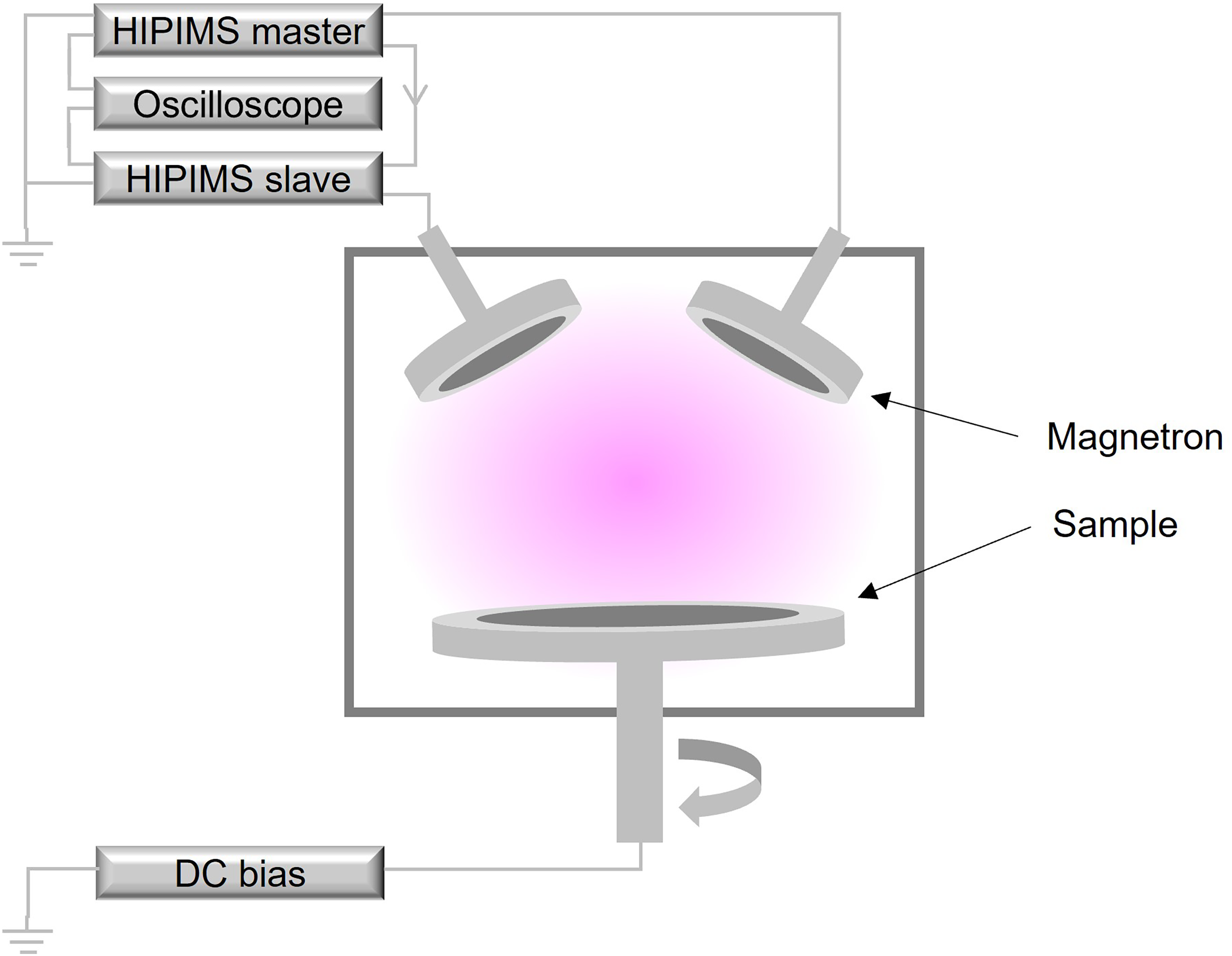
HiPIMS deposition system wiring diagram.
The system is equipped with three two-inch magnetrons and a rotary heated table. The first two magnetrons and the table are powered by a PD500X3 DC power supply (Kurt J. Lesker Company, USA) connected to an IMPULSE® pulsation unit with an Integrated Positive Kick™ (Starfire Industries, USA). The third magnetron is powered by a TRUPLASMA DC 4002 DC pulsed power supply (Kurt J. Lesker Company, USA). All the power supplies can be variously combined with the magnetrons and the table.
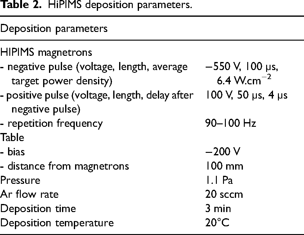
During all experiments, two magnetrons with Ti (99.95%) targets were simultaneously used. Testing of the configuration with two synchronised magnetrons was chosen with regard to industrial applications, where it is necessary to achieve a sufficient deposition rate and homogeneous coverage. The durations of the negative and positive pulses were chosen on the basis of published studies so that a sufficient number of high-energy ions were accelerated to the surface of the polymers. 14 The length of the negative pulses was set at 100 µs with a repetition frequency ranging from 90 to 100 Hz. The magnetron pulse synchronisation was provided in a master-slave mode (the master magnetron determined the same pulse frequency for the slave magnetron). The average target power density in the negative pulse was constant at 6.4 W.cm−2. In the selected tests, positive pulses with a duration of 50 μs were applied to the magnetrons with a delay of 4 μs after the negative pulses. On the table, a negative DC bias was applied. The complete deposition parameters used are shown in Table 2.
HiPIMS deposition parameters.
Both PEEK materials were used to test the effect of the positive pulse. However, only for electrically conductive CNT-PEEK, the effect of the positive pulse could be amplified by applying a negative DC bias.
The voltage and current waveforms of the magnetrons and the table were recorded with a DSO-3204 USB digital oscilloscope (VOLTCRAFT, Germany). The oscilloscope specification was: bandwidth 200 MHz, 4 channels, sampling frequency per channel 250 MSa/s, memory depth per channel 16 kpts and resolution 8 kpts. The BNC outputs of the pulsation units were connected directly to the BNC inputs of the oscilloscope set up for a 1 MΩ output impedance on a 1:1 scale. The scaling was 2.20 V indicated per the actual 1000 V on the voltage-monitor output and 1.15 V indicated per the actual 100 A on the current-monitor output.
Chemical composition
The chemical composition of the interface was determined using X-ray photoelectron spectroscopy (XPS). The depth profile of the chemical composition was analysed in individual time steps after the Ar + ion bombardment of the surface using an ion beam. The analysis was performed in a vacuum system with a basic pressure of 2–3.10−7 Pa. The system was pumped in parallel with a titanium ion pump and a turbomolecular pump. After loading the samples, the pressure was approximately 1 × 10⁻⁶ Pa and measurements were taken at this pressure. The spectra were recorded on an Omicron EA 125 hemispherical analyser in a constant transient energy mode of 20 eV. An X-ray tube with a double anode made of Al and Mg was used as the source of the primary radiation. An Al Kα line with an energy of 1486.6 eV was used for the measurements.
Results and discussion
HiPIMS pulse waveforms
The influence of ion bombardment on the formation of the Ti-PEEK interface was tested on the electrically non-conductive PEEK as well as on the electrically conductive CNT-PEEK. Samples were prepared in several different configurations, which are listed in Table 4. For each individual connection, the time course of the pulses was measured using an oscilloscope (Figure 2).
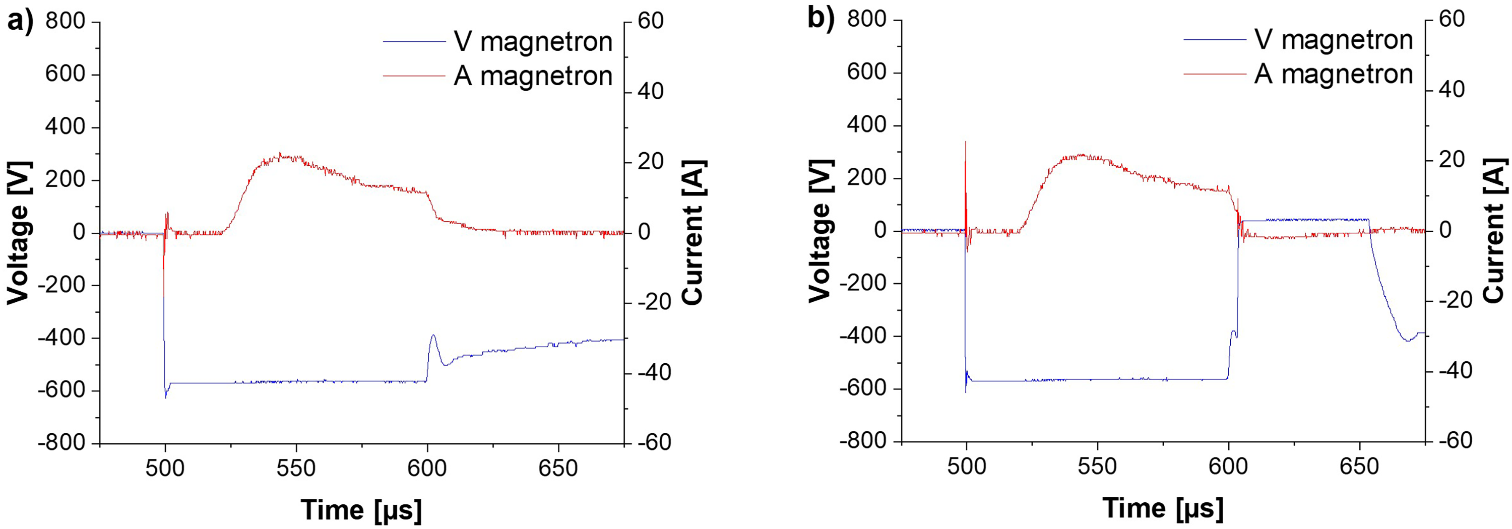
Magnetron voltage and current waveforms in HiPIMS pulses (a) without the positive pulse and (b) with the positive pulse.
The course of the negative HiPIMS pulses was measured on the master magnetron (Figure 2(a)). The pulse voltage on the magnetrons was limited to −550 V. The current in the negative pulse reached a maximum value of 21.8 A at the peaks. The voltage slowly and not immediately returned to zero after the end of the pulse. This voltage waveform was specific to this system. It may also be related to the characteristics of the pulse unit because the same voltage waveform was presented in a publication 15 in which the same pulse unit was used. If a positive pulse was used (Figure 2(b)), the positive pulses of the magnetrons started with a 4 µs delay. The positive pulse on the magnetrons was limited to 100 V, and the current in the negative pulse reached a maximum value of 22.9 A at the peak. The voltage did not return to zero after the end of the positive pulse, but dropped to negative values with a gradual return to zero.
The pulse monitoring was necessary to control the deposition process because the synchronisation of both magnetrons was very sensitive to the condition of the targets. It was important that both targets had a similar erosion zone, and thus a magnetic field. At the same time, they had to be cleaned in argon plasma for a sufficiently long time (minimum 30 min). During this time, the repetition frequency dropped from an initial value of 800 Hz to a frequency of 100 Hz, where it stabilized. Then the course of the pulses and the power on both magnetrons were the same and stable.
Chemical composition of Ti-PEEK interface
The implantation of Ti ions was followed by the deposition of the very thin Ti coating during 3 min. The surface of the samples was then gradually removed using Ar + ion bombardment. In each individual time step, an XPS analysis was performed, in which the elemental composition was determined.
In the first step, the Ar + ion etching rate of the Ti coating was determined. The Ti coating was deposited for 3 min and its thickness ranged in tens of nanometres. Such a thickness cannot be measured by the Calotest. Therefore, a reference coating deposited in 1 h was prepared. The average thickness of the Ti coating was determined from three measurements and recalculated for a deposition time of 3 min. The calculation showed that there should be a thin layer of Ti with a thickness in the range 39–44 nm (Table 4) on the sample surface. From the course of the ion etching, the time at which only the pure Ti ends was estimated. The ion etching rate of the Ti coating then corresponded to approximately 0.14 nm/min. For all of the XPS measurements, the time of the Ar + ion bombardment was converted to the depth using this speed.
Determining the depth profile of the chemical composition was very time-consuming. For the CNT-PEEK, the total etching time of all steps was up to 15 h for each sample. For the PEEK, the etching time was extended to 35 h for every sample. At the same time, it was not possible to recalculate the depth using the specified etching rate. The curves had to be fitted to the slope of the curves for the CNT-PEEK.
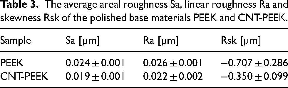
The surfaces of the base materials PEEK and CNT-PEEK were not perfectly smooth after polishing. Before ion implantation, the average areal roughness Sa, linear roughness Ra and skewness Rsk were measured (Table 3). The negative values of Rsk confirmed that scratches prevailed in the material. Therefore, the resulting implantation depth was reduced by the thickness of the mixed interface given by the Sa (Figure 3).
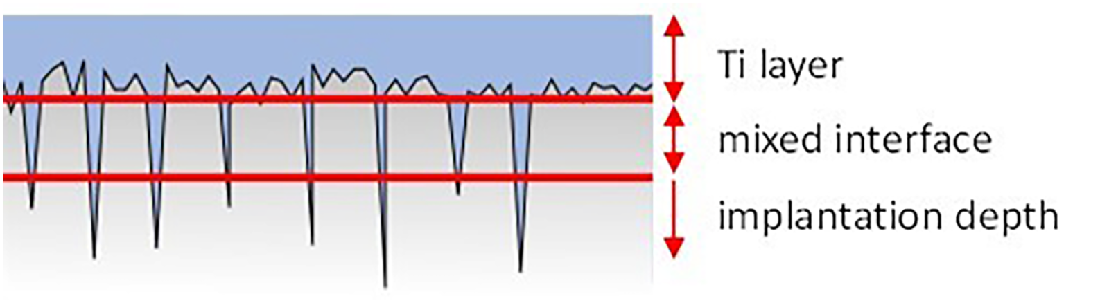
Schematic cross section of the Ti-PEEK interface. The mixed interface thickness is defined by the average areal roughness Sa.
The average areal roughness Sa, linear roughness Ra and skewness Rsk of the polished base materials PEEK and CNT-PEEK.
Electrically conductive CNT-PEEK was tested in the configuration HiPIMS pulse with a negative DC bias applied on the table. To determine the effect of the accelerating voltage, the table was first grounded. The depth profile of the chemical composition in Figure 4(a) confirmed that Ti ions were not accelerated with enough voltage given by the difference between the plasma potential and the grounding potential and the depth of implantation was detected only at the surface roughness level (Table 4). If a DC bias voltage of −200 V was applied to the table, the depth profile of the chemical composition in Figure 4(b) clearly confirmed that the Ti ions were implanted to a depth of 30 nm (Table 4). With the use of a positive pulse (Figure 4(c)), the depth of implantation of Ti ions increased to 40 nm (Table 4).
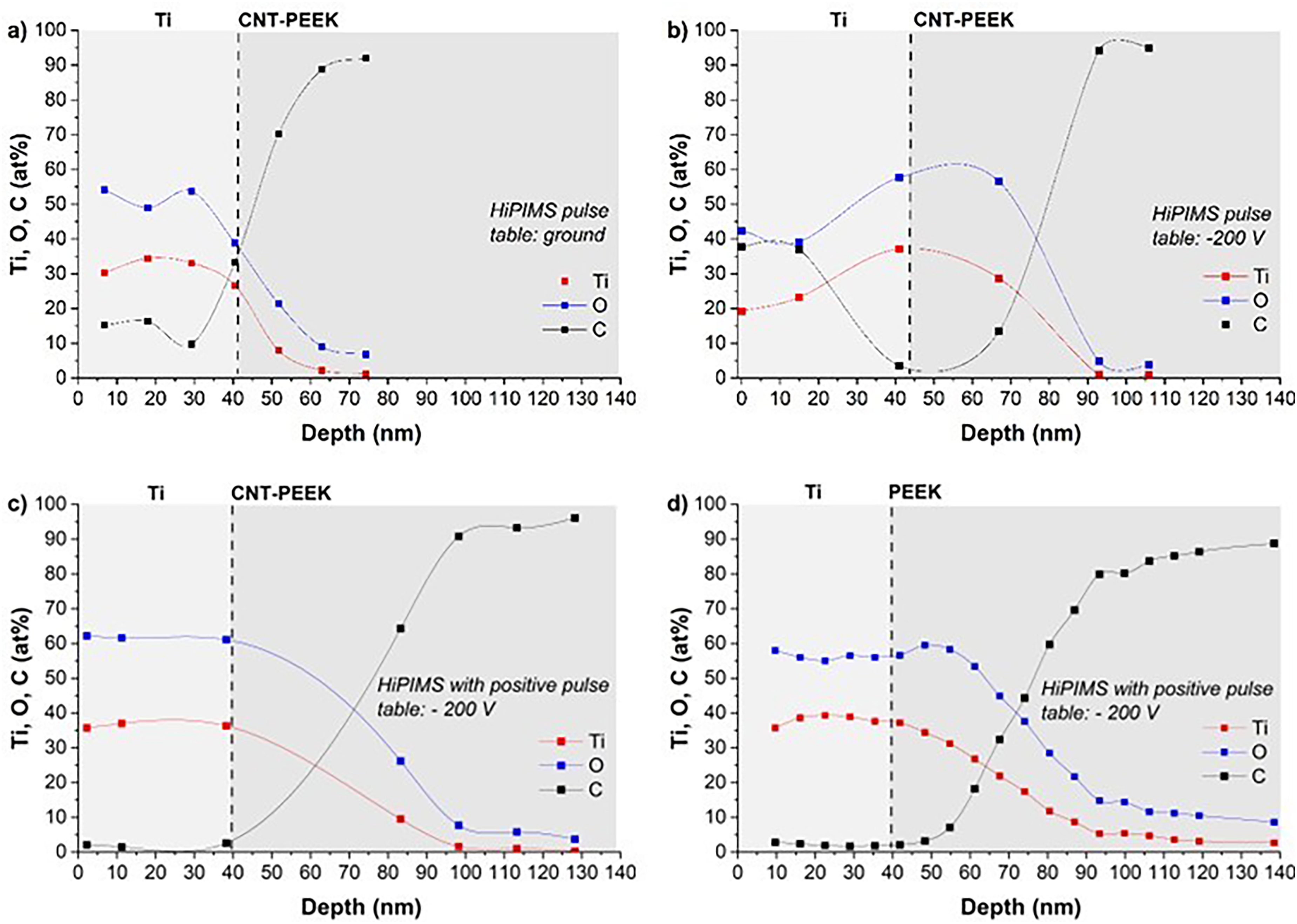
Depth profiles of the chemical composition for the conductive CNT-PEEK in configuration (a) HiPIMS pulse, table: ground, (b) HiPIMS pulse, table: −200 V, (c) HiPIMS with positive pulse, table: −200 V and for non-conductive PEEK (d) HiPIMS with positive pulse, table: −200 V.
Ti layer thicknesses and Ti implantation depths for the tested configurations of the magnetrons and the table
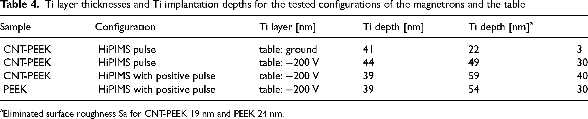
Eliminated surface roughness Sa for CNT-PEEK 19 nm and PEEK 24 nm.
Electrically non-conductive PEEK was tested in the configuration HiPIMS with a positive pulse and a negative DC bias applied on the table. In this case, negative DC bias will not affect the non-conductive PEEK but the same configuration as for CNT-PEEK was kept for comparison. The effect of the positive pulse on the implantation depth for non-conductive PEEK was similar to that used with the negative DC bias on the conductive CNT-PEEK. This is evident from the depth profile of the chemical composition for the non-conductive PEEK (Figure 4(d)), where Ti ions were detected at a similar depth of 30 nm (Table 4). The similar depth of ion implantation into polymers in the nanometre range is also mentioned in other publications for low energy ions16,17 but also for higher ion acceleration energies.18–21 The depth of implantation depends on the relative value of the stopping force. For low energy (generally in the range of 5 ∼ 500 keV) and large atomic number of the ions, the nuclear stopping is higher, it gets a maximum value in the interior of the substrate, and then decreases. 22
A positive pulse has a fundamental effect on the formation of a chemically homogeneous interface. The interface is almost sharp and consists only of Ti and O. This applies to both the non-conductive CNT-PEEK and the conductive PEEK. If only HiPIMS puls without any positive puls together with bias were used, the interface on the conductive CNT-PEEK contained C in addition to Ti and O. On the other hand, it can be seen from Figure 4(b) that the amount of Ti decreases more slowly with the depth than when a positive pulse is used (Figure 4(c)). This may be related to the formation of a sharp Ti interface on the PEEK surface, which may act, in part, as a barrier.
In order to exclude the effect of surface contamination of the samples on the chemical composition, the surface of the samples was analyzed before testing. In Figure 5 is the XPS analysis of the chemical composition, which confirmed that the surface of the samples is identical to the chemical composition of the PEEK materials. A leak in the vacuum apparatus can also be a source of impurities. A leak test was performed before heating the apparatus (1.09E 10−3 Pa.l/s) and after heating the apparatus (6.76E 10−5 Pa.l/s). In both cases, the inflow was several orders of magnitude below the flow of the working gas.
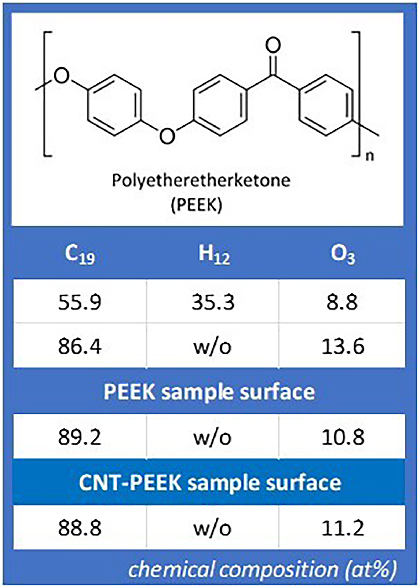
Comparison of the chemical composition of PEEK with XPS analysis of the surface chemical composition of the PEEK and CNT-PEEK samples.
Conclusions
The effect of the positive pulse on the formation of the Ti-PEEK interface was tested. Two types of PEEK materials were used as the base material, a non-conductive PEEK and a conductive CNT-PEEK. The most important findings of the experiments include the following.
The application of a positive pulse on the non-conductive PEEK has an effect on the depth of the Ti ion implantation. A positive pulse enables implantation to a maximum depth of 30 nm. If we apply a positive pulse and a DC negative bias at the same time to the conductive CNT-PEEK, the maximum implantation depth increases to 40 nm. The amount of implanted ions decreases faster with depth when a positive pulse is used. These high-energy ions accelerated in positive pulses can chemically react with the PEEK material and form a dense barrier to other Ti ions. The positive pulse applied to the conductive CNT-PEEK formed a sharp interface between the Ti coating and the PEEK material, and the coating contained only Ti and O. Without the use of a positive pulse, the negative DC bias formed an atomic inter-mixed layer, and the coating contained, in addition to Ti and O, also C originating from the PEEK material.
The HiPIMS method with a positive pulse can have a significant benefit for coating of non-conductive materials.
23
However, improving the metal coating adhesion by implantation of metal ions into the base material has a limited effect as a result of the small implantation depth. On the other hand, the formation of chemically pure interfaces can have a much greater effect in some industrial applications.
Footnotes
Declaration of conflicting interests
The authors declared no potential conflicts of interest with respect to the research, authorship, and/or publication of this article.
Funding
The authors received no financial support for the research, authorship, and/or publication of this article.