
Abstract
This paper presents a non-isolated single switch converter with high voltage gain. Its circuit topology is combined with coupled-inductor, clamp circuit, and voltage lift capacitor techniques. The proposed converter has several advantages: First, the circuit is controlled by only single pulse width modulation (PWM) for the power switch, which keeps the circuit simple. Secondly, the proposed converter is used as a clamping circuit,which let the energy of the leakage inductance can be circulated to the capacitor, so that the voltage spike on the active switch can be suppressed, and improves efficiency. This paper will introduce the principle of action, theoretical analysis, and experimental waveform in order. Finally, in the case of input voltage of 48 V, output voltage of 400 V, and output power of 1 kW, the performance of the proposed converter is verified. As a result, the maximum efficiency is up to 96.5% and full load efficiency is 92.3%.
Introduction
With the shortage of energy and forever rising oil prices, renewable energy research and green energy are becoming more and more important. These clean energies, comprising fuel cell (F.C.), wind energy, and photovoltaics (PV) can be applied as distributed generation (DG) systems. In a solar photovoltaic system, energy is generated by solar cells, and electricity is generated by converting DC to AC, so high-efficiency inverters must be used. However, inverters have some problems, such as high swithching losses, large output filter space, and many harmonics.1,2 High step-up dc–dc converters can be used in these systems as interface converters to increase the output voltage. By connecting these converters to each PV panels, they can be controlled a novel high step-up dc–dc converter was presented. The proposed converter benefits from some advantages such as low-ripple input current, high voltage gain, zero current switching of the main switch, and low voltage stress of the main switch. 3 A new method is proposed for a high-boost high efficiency converter with low swithing stress.4,5 The another presented converter is based on the SEPIC converter. However, the converter voltage gain is improved by employing a coupled inductor and two voltage multipliers. 6 Recently, DC–DC converters with high conversion ratio become popular as required in the front-end of the electrical grid supplied by environmental friendly sources of energy, or in hybrid/electric vehicles, or in data and telecommunication applications. 7 The proposed coupled-inductor-based high-gain dc-dc converter features reduced input current ripple. 8 The challenges in high step-up renewable energy applications are summarized to generate the next generation non-isolated high step-up DC/DC converters. The output voltage generated by the photovoltaic arrays, the fuel stacks, the super capacitors, or the battery sources is relatively low, even lower than 48 V. It should be boosted to a high voltage, such as 380 V for the full bridge inverter or 760 V for the half bridge inverter in the 220 V AC grid-connected power system9,10 as shown in Figure 1.

System architecture of green energy and charging station.
This paper mainly designs 48 VDC/400 VDC converters. Traditional boost converters cannot provide such high boost ratios. However, isolated converters can achieve higher voltage boost ratios through the transformer turns ratio, such as flyback converters, full-bridge converters, but isolated converters suffer high voltage spikes and high power consumption due to the leakage inductance of the transformer. In order to solve the shortcomings of traditional converters and improve conversion efficiency and voltage gain, this thesis combines switched capacitor technology, boost capacitor technology and capacitor-diode voltage multiplier technology11–13 to achieve transformerless, high boost ratio, and high efficiency DC converter.13.14
This paper proposes an integrated boost-flyback converter architecture (IBFC).12,15,16 The converters using coupled inductors can achieve high boost gain by adjusting the turns ratio, but the coupled inductors can cause leakage energy and voltage spikes. In order to solve the above two problems. This paper uses non-dissipative snubber circuit and active clamp circuit, which not only absorbs the leakage inductance energy of the coupled inductor,17–21 but also limits the leakage voltage and spike voltage stress of the active switch, thereby improving the circuit efficiency. 22
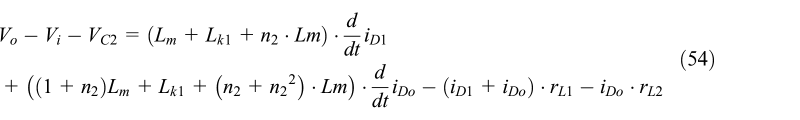
The circuit diagram of the proposed converter is shown in Figure 2. Input DC voltage Vi, power switch S1, primary side winding N1, secondary side winding N2, and third side winding N3 are winding coupling inductors, clamping capacitor C1, clamping diode D1, voltage-boost Capacitor C2, rectifier diodes D2 and Do, output capacitor Co, and output load resistance Ro. Base on the working principle, when the power switch S1 is turned on, the capacitor C2 is charged by the input power Vi, the clamp capacitor C1, the secondary side winding N2, and the third side winding N3 are charged in series. During the time interval switch S1 is off, the leakage inductance Lk1 and the magnetizing inductance Lm charge the capacitor C1. In addition, a part of the energy of the magnetizing inductor Lm is released through the secondary side winding N2 and the third side winding N3 of the coupled inductor. The energy of the DC power supply Vi, the excitation inductor Lm, the capacitor C2, and the secondary side winding N2 is charged to the output capacitor Co and the load Ro.

Proposed high step-up DC/DC converter.
Analysis of proposed high step-up DC/DC converter
Operation principle of the proposed converter in continuous conduction mode (CCM)
As shown in Figure 3, the converter operates in continuous current mode (CCM) and the waveform working principle of each point

The waveform of each point of the converter in one cycle.
According to Figure 4(a)–(f) are the six processes of the converter in continuous current mode, which are described as follows:

Current-flow path of the operating modes at CCM: (a) Mode I, (b) Mode II, (c) Mode III, (d) Mode IV, (e) Mode V, and (f) ModeVI.
Mode I [t0
Mode II [t1
Mode III [t2
Mode IV [t3
Mode V [t4
Mode VI [t5
Steady-state analysis of the proposed converter in continuous conduction mode (CCM)
In order to analyze the steady-state characteristics of the proposed converter under Continuous Conduction Mode (CCM), the following formulas ignore the leakage inductance, the Equivalent series inductance (ESL) of the inductor winding, and the Equivalent Series Resistance (ESR) of the capacitor; the capacitors C1, C2 and Co are ideal capacitors, and the coupled inductor model is Lm, And the output voltage is a fixed voltage.
As shown in Figure 5(a), the equivalent circuit when the power switch S1 is turned on, the voltage on the magnetizing inductance VLm is Vi. Current


The equivalent circuit of the proposed converter at CCM operation: (a) switch S1 turned on and (b) switch S1 turned off.
The voltage on C2 can be written as

Figure 5(b) is the equivalent circuit when the power switch S1 is off. At this time, the voltage across VLm can be expressed as

And current

According to the volt-second balance theorem, the voltage of the inductor VLm is expressed as:

The voltage which across the second-side winding VN2 and third-side winding VN3 are expressed as follows


The voltage of the clamp capacitor C1 can be denoted as

By using the volt-second balance principle, (1) and (4) the follows equation can be represented as

Substituting (5)–(8) into (9), the output voltage Vo can be derived as

The circuit of the voltage gain and duty cycle of the coupled inductor at various turns ratios is shown in Figure 6. Compared with increasing the third-side winding N3, increasing the secondary-side winding N2 can obtain a higher voltage gain.

The effect of different turns ratios on the voltage gain and duty cycle of the converter.
Effects of the ESRs on the semiconductor devices
Figure 7 shows the equivalent circuit including inductor copper inductances rL1, rL2, and rL3, on resistances of diode rD1, rD2, and rD3, and on resistance rDS(on) of the main switch. The following conditions of the proposed converter are assumed in this analysis of the Model.
The main switch parasitic capacitor and the diode capacitor are excluded.
During the switch is turned on can be modeled a resistance rDS(on), and during the switch turned off can be modeled an infinite resistance.
The diodes are modeled by the forward voltage VD1, VD2, and VDo, and the forward resistances rD1, rD2, and rDo. When the diodes are reversed-biased they can be modeled by an infinite resistance.
The effect of leakage inductances Lk1, Lk2, and Lk3 are neglected.
Switching loss and ESRs of capacitors are neglected.
Assumed the magnetizing inductor is sufficiently large to ensure a small-ripple current approximation.
To consider DC components during the off period, the average current is IL1 = iL1(t), and the average current is IL2 = iL2(t).
The capacitors C1, C2, and Co are assumed to be large enough and output voltage Vo is constant.

Equivalent circuit with copper and semiconductor losses.
Based on the Kirchhoff’s voltage law (KVL) principle, during the switch S1 is turned on as shown in Figure 8(a), the following equations can be represented as follow


where


Equivalent circuit: (a) switch turned on and (b) switch turned off.
The current of output capacitors CO, C1, and C2 are given as follows:


During the main switch S1 is turned off as shown in Figure 8(b), the following equations can be represented as follow


The current of C1, C2, and output capacitor CO are givens as follow


Substituting (13) into (18), the inductor voltage VL1(off) is derived as

Based on the amp-second balance principle, from (14)–(16) and (19)–(21) can be rewritten as follows:


According to (25), the current flow path the Co can be presented as

Form equation (26), the current iL2 is determined as

According to (23), the current flow path the C1 can be presented as

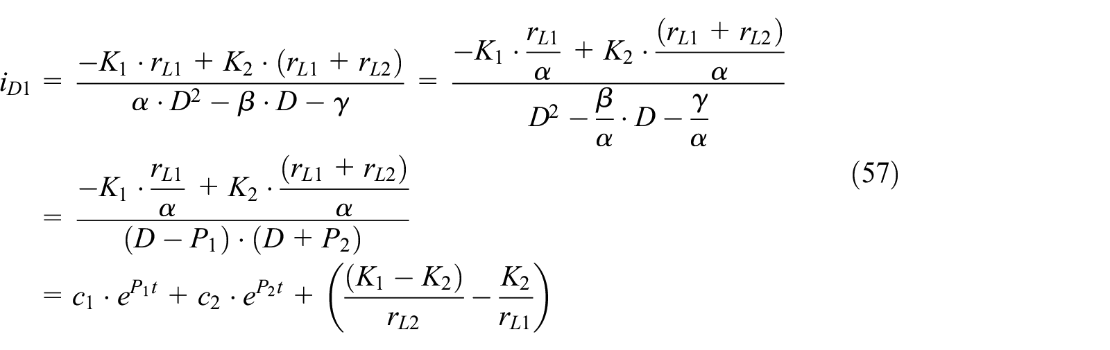
Form equation (28), the current iD1 is determined as

According to (27) and (29), the current flow path the iL1 can be derived as follows


From (27) and (31), iL1 can be rewritten as

Where in the steady state, the principle of volt-second balance can be given as equation:

Where
Substituting (32) into (33), the equation can be rewritten as

Substituting (31) into (34), the proposed converter output voltage VO is derived as

Where
and
From equation (35), the voltage conversion ratio VO/Vi is represented as follows:

Where
The voltage gain and efficiency affected by different ESRs with coupled-inductor is shown in Figure 9. It can be seen that increase the equivalent series resistance rL1 is obtained lower voltage gain than increase the equivalent series resistance rL2 or rL3. The maximal voltage gain is constrained by the equivalent series resistances, and the efficiency will be decreased by the extreme duty ratio.

Voltage gain versus duty ratio and efficiency versus duty ratio under different ESRs with coupled-inductor.
Neglecting the equivalent series resistance of the proposed converter, the ideal voltage gain can be expressed as

According to (36), the equation can be reorganized and the equivalent circuit is shown in Figure 10 as follows

Where
and

Equivalent circuit corresponding to equation (54).
The input power and output power of the converter can be calculated as shown in equation (39) and (40), respectively.


According to the equations (39)–(41), the converter efficiency can be derived as follows
Where
and
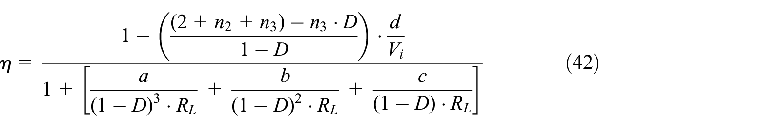
From equation (42) shows that the efficiency is affected by the equivalent series resistance. Figure 11 shows the voltage gain and efficiency affected by various turns ratios and ESRs.
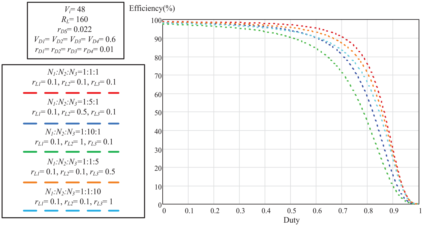
The efficiency versus duty ratio under various turn ratios and ESRs.
To analysis of the effect on leakage inductance and winding resistance leads to the current waveform being exponential functions at the off period of the switching cycle, as shown in Figure 12.

The equivalent circuit during switch S1 turned off period.
The maximal magnetizing current at ton as follow

The magnetizing current during switch S1 in turned off can be given as follows:


Substituting equations (45) into (44) derived as

During switch S1 in turned off, the voltage across the magnetizing inductor VLm and leakage inductance Lk1 can be expressed as


The voltage across the secondary winding VL2 and the leakage inductance Lk2 can be expressed as


Based on the Kirchhoff’s voltage law (KVL) to find the inductor voltage during the switch S1 is turned off period of each cycle is represented as follow:

Then

Therefore
The other loop of current id1 flow through D1 to charge the clamped capacitor C1, the equation can be represented as:


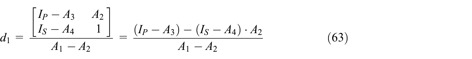
According equations (54) and (55) in matrix form can be rewritten as

From equation (56), by using the Kramer Law to solving of the iD1 and iDo can be derived as follow:

Where:
and
and
and
Substituting equations (57), (58) into (55) is obtained the following


Substituting equations (59) and (60) into (57) and (58) given as

Where:
From equation (61) the initial current of iD1 and iDo are as follow respectively:

By solving the equation (62) can be derived as follow:
From equation (56) that the ESRs are neglected, the off period current id1 and ido can be derived as

According to equations (57) to (65), the diode currents iD1 and iDo are exponential due to the R-L circuit formation between the equivalent series resistances and the leakage inductances. The diode current waveforms iD1 and iDo are shown in Figure 13.
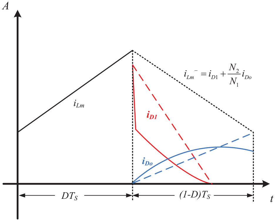
During off-period corresponding diode currents.
Analysis of voltage stress of the power devices
The voltage stress is an important issue related to the cost and efficiency of converter. Due to low voltage rating and low rDS(on) of power switch can be utilized in the circuit. Therefore, the switching and conduction losses can be reduced. In addition, the lower cost and higher efficiency of the converter can be received.
The voltage stress across power switch VDS can be equaling the summation of DC-source Vi and magnetizing inductor voltage VLm in turned off period. Therefore, the voltage stress across power switch S1 is


While the switch S1 is turned on, the diodes D1 and Do are reverse-biased. Therefore, the voltage stresses of diodes D1 and Do is as follows


While the switching S1 is turned off, the diode D2 is reverse-biased. Therefore, the voltage stresses across D2 is as follows

Experiment of the proposed converter
The converter is tested to operate at the 48 V dc-input voltage and the switching frequency fs is 50 kHz. The output voltage and output power are specified as Vo = 400 V and Po = 1 kW respectively, and by using the current mode PWM IC UC3845 to achieved performance of the circuit. From the above design procedure, the power switch is selected as IXFH120N20P which has low ON state resistance rDS(on) of 22 mΩ and is rated at 200 V. The winding N1:N2:N3 is obtained as 1:1:2. The diode D1 selected as B30H150G is Schottky diode and is rated at 150 V, 30 A. The voltage stress of voltage diodes D2 and DO are larger than D1. Schottky diodes are not suitable for utilized. Therefore, diodes D2 and DO are selected as fast diode DSEI8-06A which are rated at 600 V, 8 A. Table 1 lists the main components and parameter requirements for the prototype.
Components and parameters in the proposed converter.

This section introduces the voltage waveform and current waveform at each point of the converter under a full load of 1 kW. Figure 14 shows the converter’s magnetizing inductance current iLm and the power switches VGS and VDS.

Experimental coupled-inductor current and power switch voltage waveforms under various output power: (a) 250 W, (b) 500 W, (c) 750 W, and (d) 1 kW.
And as shown in Figure 15, when the output voltage VO = 400 V, the power switch VDS can be clamped to avoid high voltage stress. The voltage across the diodes D1, D2, and DO are shown in Figure 16.

Experimental switch voltage when Vi = 48 V and PO = 400 V.

Experimental voltage across diodes D1, D2, and DO of the proposed converter with VO = 400 V and PO = 1 kW.
The cut-off voltage of VD1 and VDO is less than the output voltage. The clamping circuit of the charging current iD1 is shown in Figure 17(a). The inrush current is caused by the leakage inductance of the coupled inductor while the power switch turned-off. Furthermore, the leakage inductance energy is recycled to the capacitor C1 for further improve the efficiency of the converter. Figure 17(b) shows that the current iD2 of the secondary-side winding N2 is connected in series with voltages Vi, VC1, and VN3 to charge capacitor C2. Figure 17(c) depicts the output current iDo of the energies of Vi, Lm, C2, and N2 charge output capacitor Co and load Ro. As shown in Figure 18, the efficiency of the converter under different output powers PO, where the maximum efficiency is about 96.5% at 200 W, and the efficiency is about 92.3% at a full load of 1 kW.

Experimental current flow through diodes of the proposed converter with VO = 400 V and PO = 1 kW: (a) D1, (b) D2, and (c) DO.
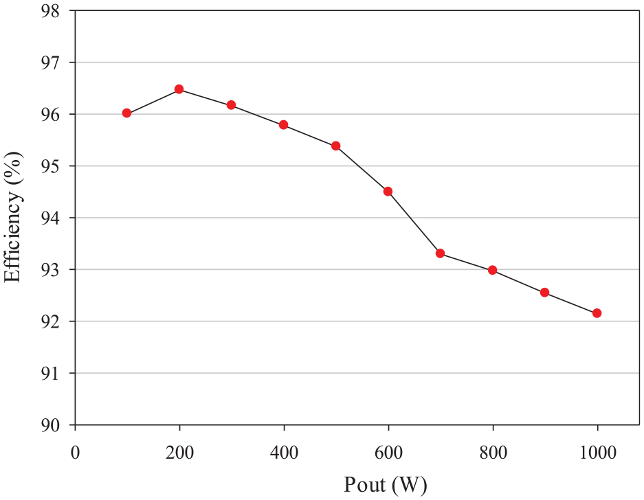
The conversion efficiency with Vi = 48 V and Vo = 400 V under various output power (Pout).
Conclusion
This paper proposes a non-isolated high-boost DC/DC converter. The converter architecture combines switched capacitor technology, boost capacitor technology, and capacitor diode voltage doubler technology, not only can recover the leakage inductance energy on the coupled inductor, improve the conversion efficiency, but also has a higher voltage gain. In addition, the active clamp circuit limits the peak voltage on the VDS of the power switch, reducing the voltage stress of the power switch. Based on the above conditions, this paper proposes that the converter architecture achieves high voltage gain, high efficiency, and effective suppression of voltage stress, and can be effectively applied to the conversion system of green energy grids and electric vehicle charging station.
Footnotes
Declaration of conflicting interests
The author(s) declared no potential conflicts of interest with respect to the research, authorship, and/or publication of this article.
Funding
The author(s) disclosed receipt of the following financial support for the research, authorship, and/or publication of this article: This research was sponsored by Ministry of Science and Technology of Taiwan under the Grant MOST108-2221-E-150-046 and NFU 108B1-061.