
Abstract
Electronic skin (e-skin) has shown great application prospects in many fields due to its multiple advantages. Previous studies have illustrated that the structure with a dielectric layer sandwiched between two electrodes had good pressure-sensing abilities, and microstructures in the dielectric layer could improve the sensitivity. In this paper, we proposed mechanical models of e-skin sensing unit with different microstructures (flat, trapezoidal, half-cylinder, and pyramids) in the dielectric layer. Then, we performed finite element method simulations and experiments to validate the model. Finally, we demonstrated its application as the pressure-sensing unit for human hands, showing its great potentials in sensors of artificial prosthesis or soft robots in the future.
Introduction
Skin is an important media for humans to perceive the environment. Its powerful sensing ability can help people to understand the shape, surface features, and contact patterns of the contact objects. However, some accidental skin injuries even amputations could lead to impaired sensing ability of the skin and may lead to dangers. Sensors worn on the skin can compensate for sensing defects caused by skin injuries and help humans to avoid potential dangers while improving the quality of life. 1 So far, artificial prostheses and data gloves applied to Virtual Reality (VR) systems have been able to mimic certain mechanical and biological properties of the human body2–4 and achieve the sensing ability of the skin to some extent. However, the applications of traditional sensors in this field are limited due to their special design requirements such as weight, cost, and durability. E-skin, as a new type of sensor based on flexible materials, has the advantages of lightweight, strong environmental adaptability, simple structure, and excellent biocompatibility. 5 These advantages can be well applied in the design and fabrication of auxiliary sensing system of artificial prosthetics 6 as well as other health care applications. 7
Parallel-plate capacitive e-skin has the advantages of small temperature coefficient, good output stability, fast dynamic response, low power consumption, and so on. It has a wide range of applications in the fields of personalized health monitoring 8 and biomechanics, as well as artificial prostheses. The most popular structure used in capacitive e-skin is polydimethylsiloxane (PDMS)/Ecoflex dielectric layer sandwiched between two electrodes because of its easiness of preparation and simplicity of data acquisition.9,10 Previous studies have shown that adding proper microstructures in the dielectric layer can effectively improve the sensitivity of the sensing unit, and different shapes and sizes of microstructure have a significant impact on it as well (flat, 11 trapezoidal, 12 half-cylinder, 13 and pyramids 14 ). However, most research investigated the sensing ability through experiments. Few articles have analyzed the effect of different microstructures theoretically. The underlying mechanisms are not well studied yet, which are critical to the design of parallel-plate capacitor–based sensors and their further applications.
In this paper, we conducted both modeling and experimental studies of capacitive pressure sensors with microstructured dielectric layers. Mechanical models of e-skin sensing unit with four kinds of microstructures (flat, trapezoidal, half-cylinder, and pyramids) in the dielectric layer were studied and found that e-skin sensing unit with pyramids microstructure had the highest pressure-sensing sensitivity. In order to validate these models, finite element method (FEM) simulations and experiments were conducted. After that, we successfully applied an e-skin sensing unit with pyramids microstructure as a pressure sensor on a human fingertip to demonstrate its application potentials. In this work, methods including mathematical modeling, FEM simulations, and experimental tests were conducted to systematically study the sensing mechanisms of the parallel-plate capacitive pressure-sensing unit, providing guidance for future e-skin designs and applications.
Mechanical model of the sensing unit
We use polyethylene terephthalate (PET)/indium tin oxide (ITO) film as the upper and bottom electrodes of the capacitor. Its Young’s modulus is 4000 MPa, which is much larger than that of the PDMS dielectric layer (2.215 MPa, weight ratio was 10:1 of the base polymer and the curing agent). Therefore, the deformation of electrodes is far smaller than that of PDMS, which can be ignored in calculations.
Take the sensing unit with pyramid microstructures as an example, 15 the force analysis is shown as Figure 1. The edge length of the top and bottom square are Xm and XL, respectively. The height and the thickness of the microelement layer are hm and dhm, respectively. The angle between the side and bottom edge is α.
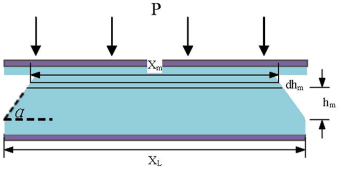
Force analysis of the pyramid microstructured dielectric layer.
The pressure applied on the top surface of the sensing unit is considered as a uniform pressure P, and the normal force transmitted to the top surface of the pyramid microstructure is

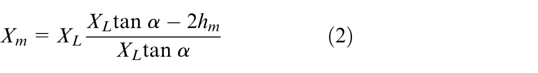
As shown in Figure 1, the microelement layer is selected where its height is hm, the thickness of the microelement layer is dhm, and the edge length of the microelement layer is calculated as
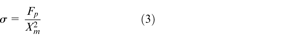
Since the pressure on the top electrode is uniform, it is assumed that the stress distribution is uniform on the pyramid plane parallel to the top surface, and the stress is calculated as
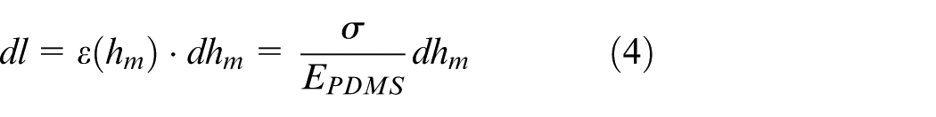
According to the stress–strain relationship of the elastomer, the compression of the microelement layer is calculated as
Considering PDMS as a linear elastic material, its Young’s modulus is a constant. From equations (1)–(4), the total compression of the pyramid microstructure is calculated as

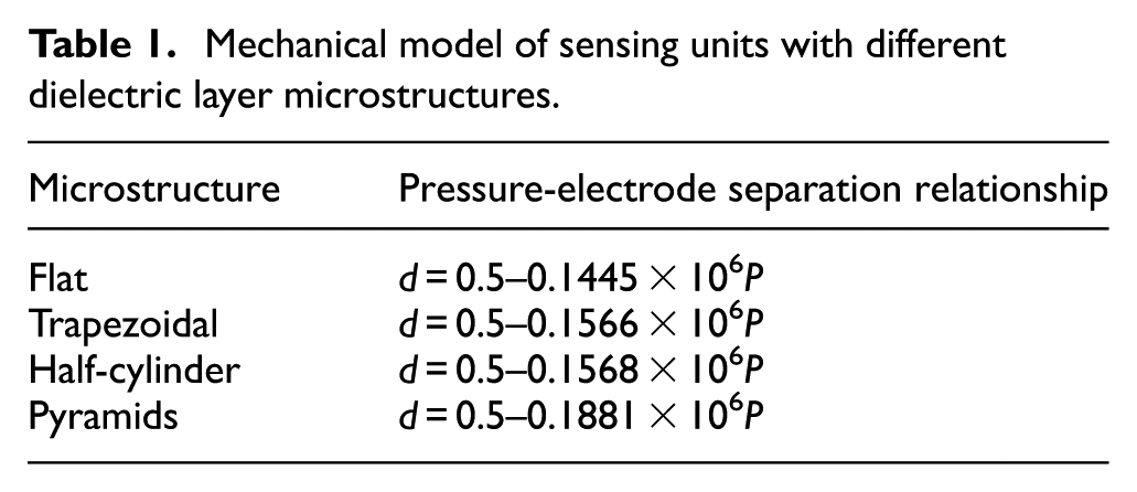
The mechanical models of the other three microstructures can be achieved through the same way, which is not discussed in detail here. By substituting the parameters, the pressure-electrode separation relationships of e-skin sensing units with different dielectric layer microstructures are shown in Table 1, where P is the pressure applied on the top of the sensing unit and d is the calculated electrode separation.
Mechanical model of sensing units with different dielectric layer microstructures.
FEM analysis
In order to validate the mechanical model of the e-skin sensing unit, the static structural FEM simulation (ANSYS, Pittsburgh, PA, USA) was used to study the pressure-sensing ability of the e-skin sensing units. Simulations were conducted using Solid 138 element. The structure of the model consisted of two electrodes (PET) sandwiching the dielectric film (PDMS). The simulation parameters 16 are shown in Table 2.
Parameters in FEM simulation.
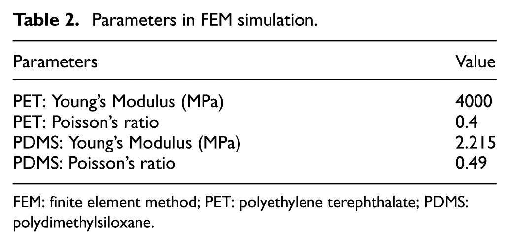
FEM: finite element method; PET: polyethylene terephthalate; PDMS: polydimethylsiloxane.
A single microstructure was used in the simulation to simulate the actual e-skin sensing unit. The initial electrode separation is d0 = 0.5 mm. A single microstructure was used to simulate the actual e-skin sensing unit. The initial electrode separation is α = 70.07°. The bottom side length (or diameter for the half-cylinder) is XL = 1 mm. Meanwhile, because of the nature of the soft imprinting fabrication process of these PDMS microstructures, there is always a thin flat layer of PDMS at the bottom of the fabricated dielectric film 17 after demolding, which are considered in the simulations. The initial height ratio of the microstructure to the total height of the dielectric layer is d0/dh = 0.32/0.5 = 64%. The simulation models of e-skin sensing units with different dielectric layer microstructures are shown in Figure 2.
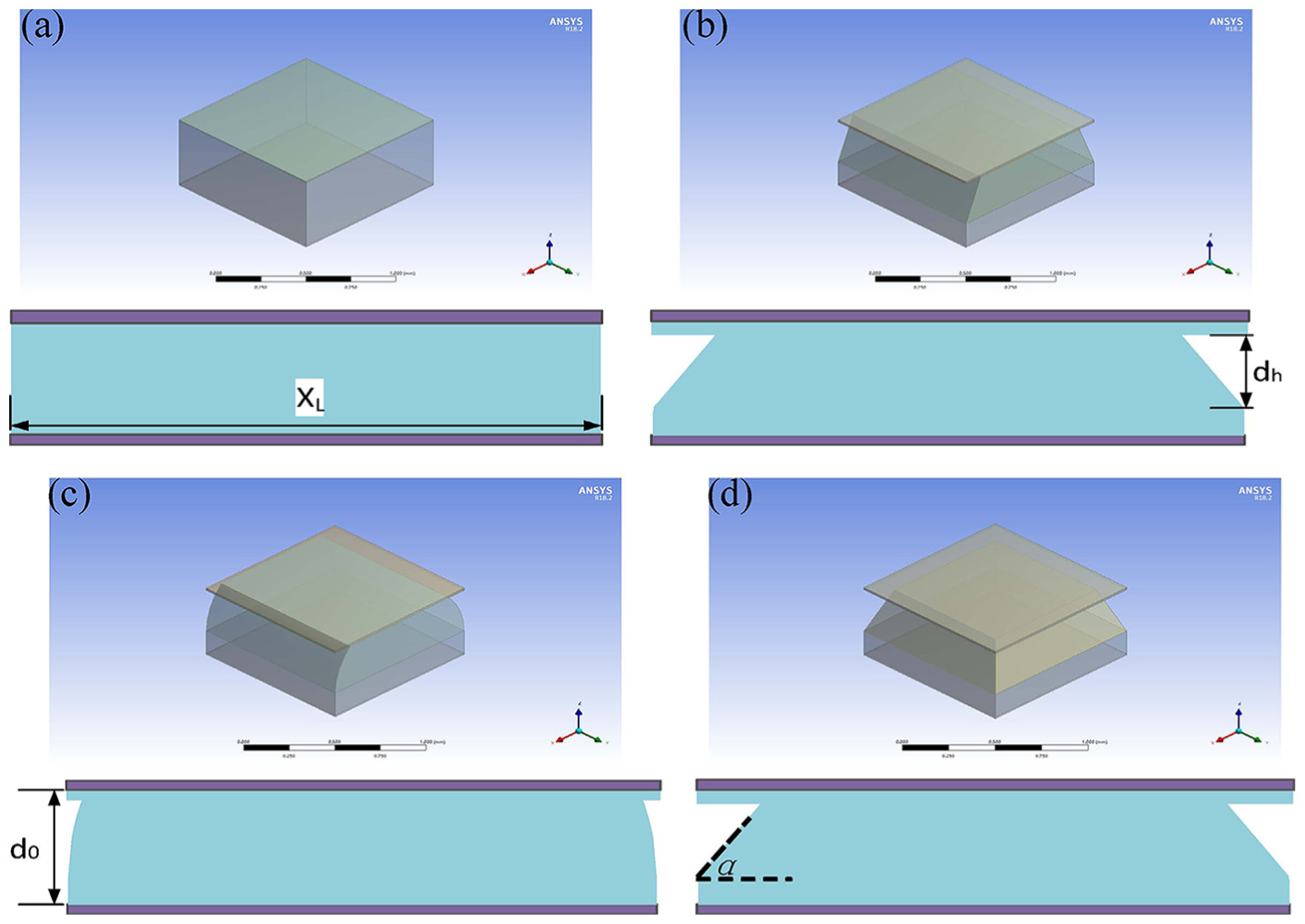
Simulation models of e-skin sensing units with different dielectric layer microstructures: (a) flat structure, (b) trapezoidal microstructure, (c) half-cylinder microstructure, and (d) pyramids microstructure.
In order to validate the mechanical model of the e-skin sensing unit, we compared the simulation results with the mechanical models (Figure 3), and the maximum relative errors of the four models are 0.2%, 0.55%, 0.54%, and 0.46%. As introduced above, Young’s modulus of the PET/ITO electrodes was much higher than the rest of the capacitor, which were neglected in the mathematical models for simple calculations. Due to its easy implementation, the electrode deformations were considered in the FEM simulations, to better simulate the sensor’s mechanical behaviors. Therefore, the fitting errors between the mechanical models and the simulations were caused. Nevertheless, these errors were all less than 1%, which were acceptable for understanding the sensing mechanisms of the unit.
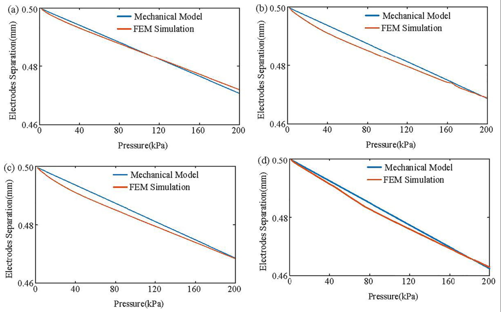
Comparisons of mechanical models and simulation results: (a) flat structure, (b) trapezoidal microstructure, (c) half-cylinder microstructure, and (d) pyramids microstructure.
Effects of different dielectric layer microstructures were then studied. As shown in Figure 4(a), the electrode separation decreased more with pressure for the microstructured dielectric layers than that with a flat dielectric layer, and that with micropyramids decreased the most among them. By obtaining the capacitances through the parallel-plate capacitance formula C = εrε0A/d (where εr = 2.7 is the relative dielectric constant of PDMS, 18 ε0 = 8.85 × 10⁻¹² F/m is the permittivity of free space, and C0 = 10.76 pF is the initial capacitance of the sensing unit without pressure), the pressure–capacitance relationships and pressure–relative capacitance change relationships of e-skin sensing units with different dielectric layer microstructures are shown in Figure 4(b) and (c), respectively. Clearly, both the capacitance and the relative capacitance change increased more with pressure for the microstructured dielectric layers than those with a flat dielectric layer, and those with micropyramids increased the most among them. It can be concluded that the pressure-sensing sensitivity of the e-skin sensing unit with microstructured dielectric layer was better than that with a flat dielectric layer. Among different microstructures, the pyramid microstructure increased the sensitivity of the e-skin sensing unit the most.
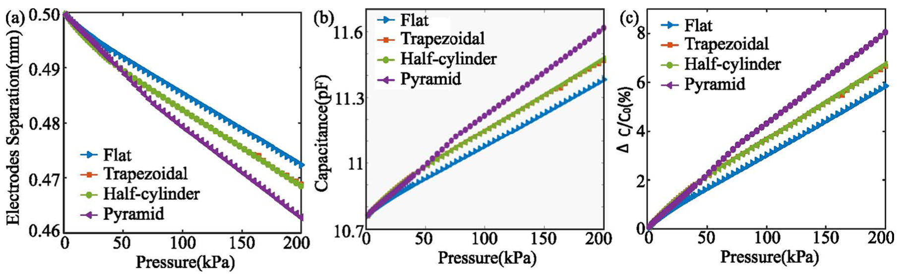
Simulated relationships between pressure and (a) the sensing units’ electrodes separations, (b) capacitances, and (c) relative capacitance changes. The dielectric layers of these sensing units consisted of four different kinds of microstructures: flat, trapezoidal, half-cylinder, and pyramid. The sensing unit with pyramid microstructured dielectric layer showed the highest pressure-sensing sensitivity.
Experiments and discussion
Uniaxial tension test
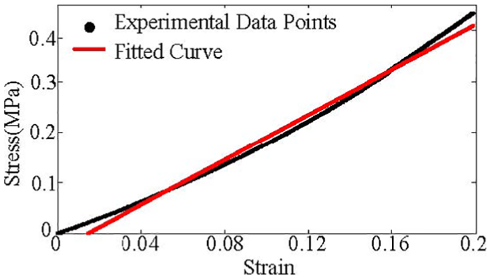
The mechanical properties of the PDMS are closely related to the ratio of the base polymer to the curing agent. Young’s modulus of PDMS can be adjusted by changing the mass ratio of the two materials (0.55−3 MPa). In the experiment, the international standard uniaxial tension test (ISO 37:2005, type 3) was performed on the PDMS sample (10:1 of the base polymer and the curing agent) using a SUNS universal testing machine (UTM2502; SUNS, Shenzhen, China). The relative errors of the stretching machine were ≥±0.13% and ±0.12% for the force and displacement, respectively. The stretching speed was 500 mm min−.
The strain–stress curve obtained through the uniaxial tension test is shown in Figure 5. A fitted linear relationship between the strain (ε) and the stress (σ) can be obtained as

Uniaxial tensile test results. The test data points and fitted line.
Therefore, Young’s modulus of the PDMS sample was 2.215 MPa, and Poisson’s ratio was 0.49. In this fitting, we treated the PDMS as a linear material for simplification. As a high polymer, nonlinear characteristics of this material may well affect the mechanical behaviors, 17 which contributes to the fitting errors. Nevertheless, the R2 = 0.990 for this fitting, indicating a reasonable representative of its mechanical property.
Sensing units’ fabrication
In order to validate our models, e-skin sensing unit with flat structure and pyramids microstructure were fabricated. A commercial precision abrasive sheet (268XA; 3M, Minnesota, MN, USA) was used as the mold, which was covered with squared pyramids of 0.32 mm in height on one side (Figure 6(a)). The obtained dielectric film with pyramid microstructures is shown in Figure 6(b). The mass ratio of the base polymer to the curing agent was 10:1 for the preparations of our PDMS (SYLGARD 184; Dow Corning, Michigan, MI, USA) samples.
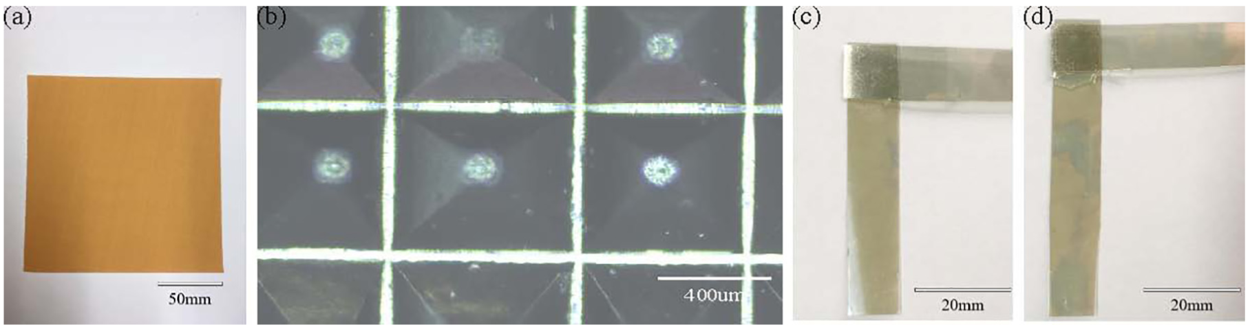
(a) PDMS mold, commercial precision abrasive sheet (268XA; 3M), (b) dielectric film with pyramid microstructures, (c) e-skin sensing unit with a flat dielectric layer, and (d) e-skin sensing unit with the dielectric layer of micropyramids.
The fabricating process of the e-skin sensing unit is illustrated in Figure 7. In order to prepare the dielectric film with microstructures, 3.7 g fully mixed PDMS was evenly poured on the mold, and the mold with the PDMS was left for 24 h at the room temperature of 23 °C to be half cured. After that, a PET/ITO film (NOZO Tech, Luoyang, China) was attached onto the PDMS film as the bottom electrode and left at room temperature (23 °C) for another 24 h to be fully cured. After the PDMS and bottom electrode was peeled off from the mold, another PET/ITO film covered with thin layer of PDMS mixture was attached onto the other side of PDMS as the top electrode and left to cure. Details of this fabrication process are described in our previous work. 17 The completed e-skin sensing unit is shown in Figure 6(c) flat dielectric layer and (d) micropyramids in the dielectric layer. And, the parameters of the experimental sensing unit are shown in Table 3.
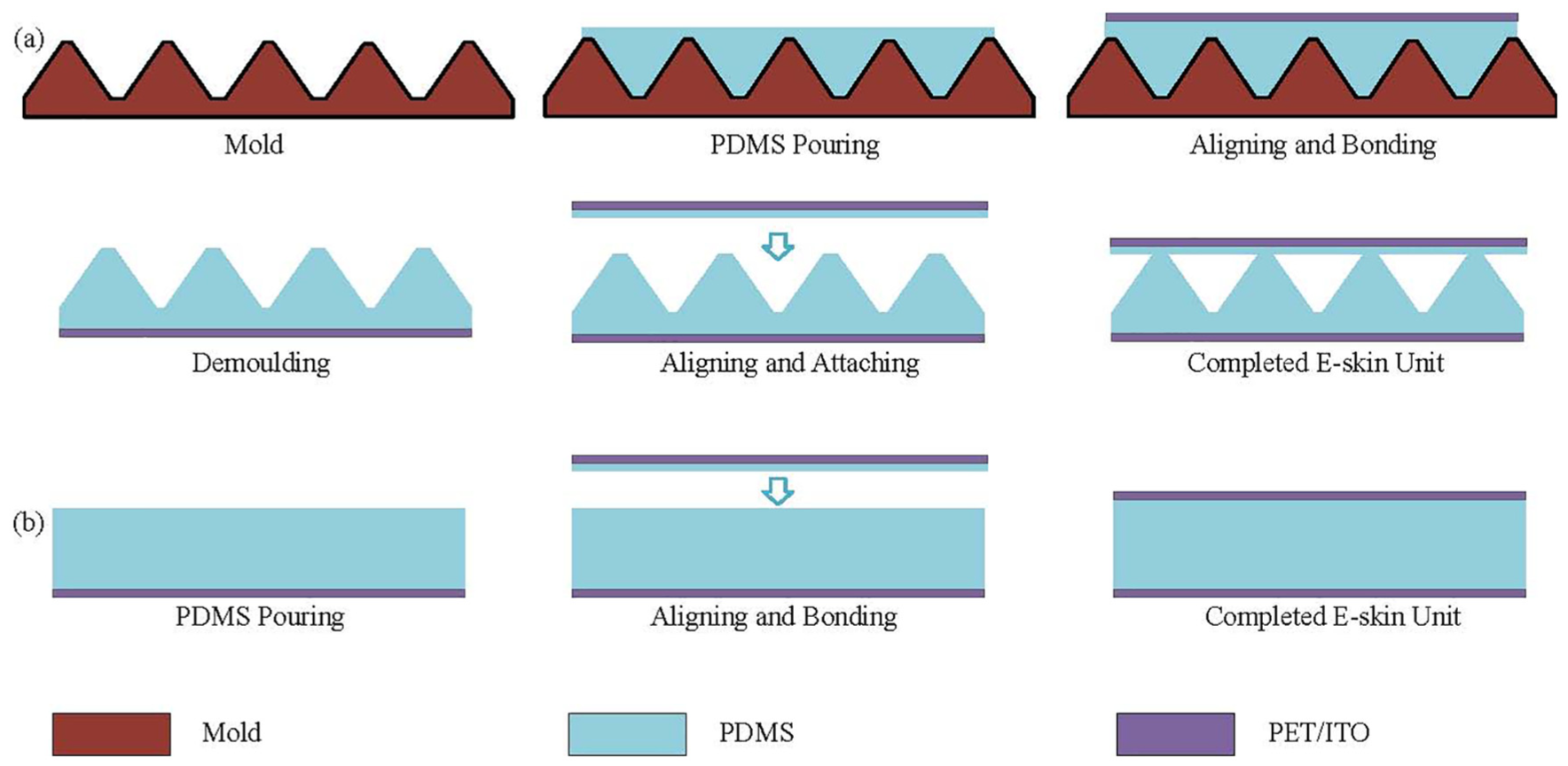
Fabricating process of e-skin sensing unit, (a) e-skin sensing unit with micropyramids in the dielectric layer: pour the PDMS (10:1) on the mold and attached the bottom electrode to cure together, then attach the top electrode after peeling off to complete the fabrication. (b) e-skin sensing unit with flat dielectric layer: pour the PDMS (10:1) on the bottom PET/ITO and then attach the top electrode after 48 h when it was cured to complete the fabrication.
Experimental parameters of e-skin sensing units.
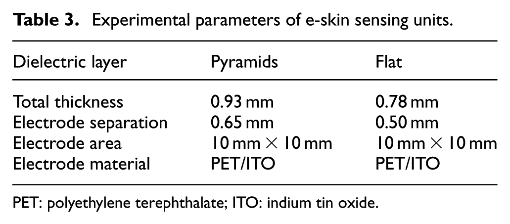
PET: polyethylene terephthalate; ITO: indium tin oxide.
Measurement setup
The block diagram of the measurement system is shown in Figure 8. The data acquisition circuit included a 32-bit microcontroller (STM32F103IGT6; STMicroelectronics, Geneva, GVA, Switzerland) and a serial-to-USB module (CH340G; Qinheng, Nanjing, China). The capacitance measurement module was a capacitance digital converter AD7746 (Analog Device, Norwood, MA, USA) and a self-made range expansion module based on the operational amplifier AD8515 (Analog Device). The AD7746 generated a square-wave excitation signal to the measured capacitance Cx and the modulator continuously sampled the charge going through the Cx. The data from the digital filter were scaled and transferred through the I2C bus to the microcontroller. Therefore, its original measurement range was −4.096 ∼ 4.096 pF. In order to expand its measurement range for our studies, a Range Expansion Module based on AD8515 was employed. This module reduced the excitation voltage of the AD7746 by P times (12.111 times in this work) and expand the measurement range to 0 ∼ 99.213 pF.
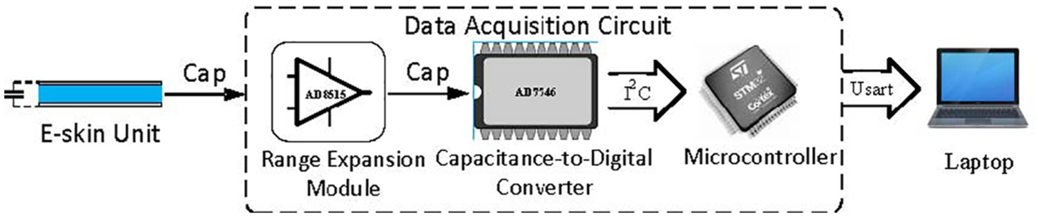
The block diagram of the measurement system of e-skin sensing unit.
Sensing abilities
We prepared e-skin sensing units with flat structure and micropyramids in the dielectric layer for the experiments to study their pressure-sensing abilities. The micropyramids were selected rather than other microstructures, due to the outstanding pressure-sensing sensitivity of the e-skin sensing unit with micropyramid dielectric layer. In order to apply the external pressures, we used nine masses weighted from 1 to 2 kg as loads on the top surface (surface area: 10 mm × 10 mm), and the corresponding pressures were 98 ∼ 196 kPa. The relationships between the pressures and the capacitances are shown in Figure 9(a), and the relationships between pressure and relative capacitance changes are shown in Figure 9(b).
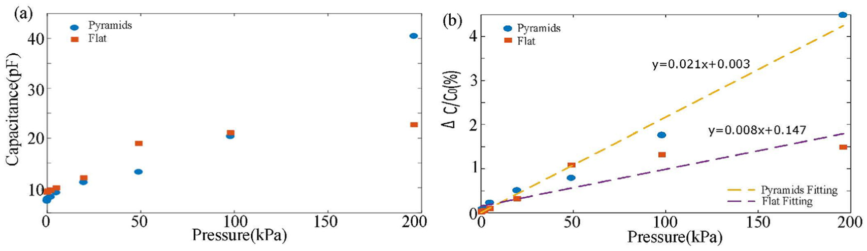
Experimental relationships between the pressures and the e-skin sensing units’ (a) capacitance and (b) relative capacitance changes. The dielectric layers of these sensing units consisted of flat structure and micropyramids. The slope of the fitted curve in (b) is expressed as the pressure-sensing sensitivity of the e-skin sensing units, and the unit with micropyramids in the dielectric layer had a higher sensitivity (S = 0.021 kPa−) than that with a flat structure (S = 0.008 kPa−).
In addition, the sensitivity of capacitive pressure sensors S can be expressed as
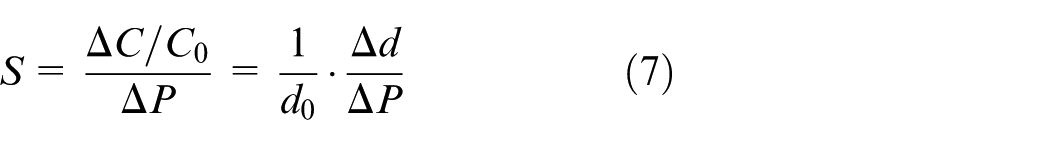
where C0 is the initial capacitance without pressure; d0 is the initial electrode separation; ΔC, Δd, and ΔP are the changes of capacitance, electrode separation, and pressure on the top, respectively. It can be seen from Figure 9(b) that e-skin sensing unit with micropyramids in the dielectric layer had higher sensitivity than sensing unit with flat dielectric layer (S = 0.021 kPa− vs S = 0.008 kPa−). The presence of air in the gaps among micropyramids could be one reason leading to the high pressure-sensing sensitivity. The elastic resistance of air was much smaller than that of a solid flat structure, which was easier to compress (reduce in electrode separation). At the same time, the volume proportion of air to the dielectric layer decreased with the electrode separation reduction caused by normal force, because the air could be squeezed out during this process. Since the relative dielectric constant of the air (ε0 = 1.0) is significantly smaller than that of PDMS (εr = 2.7), the overall relative dielectric constant of the microstructured dielectric layer would increase with pressure caused electrode separation. Therefore, more reduction of the electrode separation and higher relative dielectric constant during compression would make the capacitance of the e-skin unit with the dielectric layer with micropyramids more sensitive to normal pressures.
Application
Because of its pressure-sensing ability, the e-skin can be applied in the auxiliary sensing system of artificial prosthetics. In order to demonstrate its application potentials, we attached the e-skin sensing unit with micropyramids in the dielectric layer to a human fingertip and monitored its pressure variances during a mug handling process. Based on the changes of capacitance (Figure 10(a)), the hand motions (Figure 10(b)–(e)—approaching, touching, holding, and releasing, respectively) could be clearly differentiated. Response times of the sensing unit were not considered for now. The dynamic sensing properties are important to the application of this sensing unit. They would be affected by the material properties and mechanical dimensions of the unit itself and the signal processing strategy, which will be studied in the future.
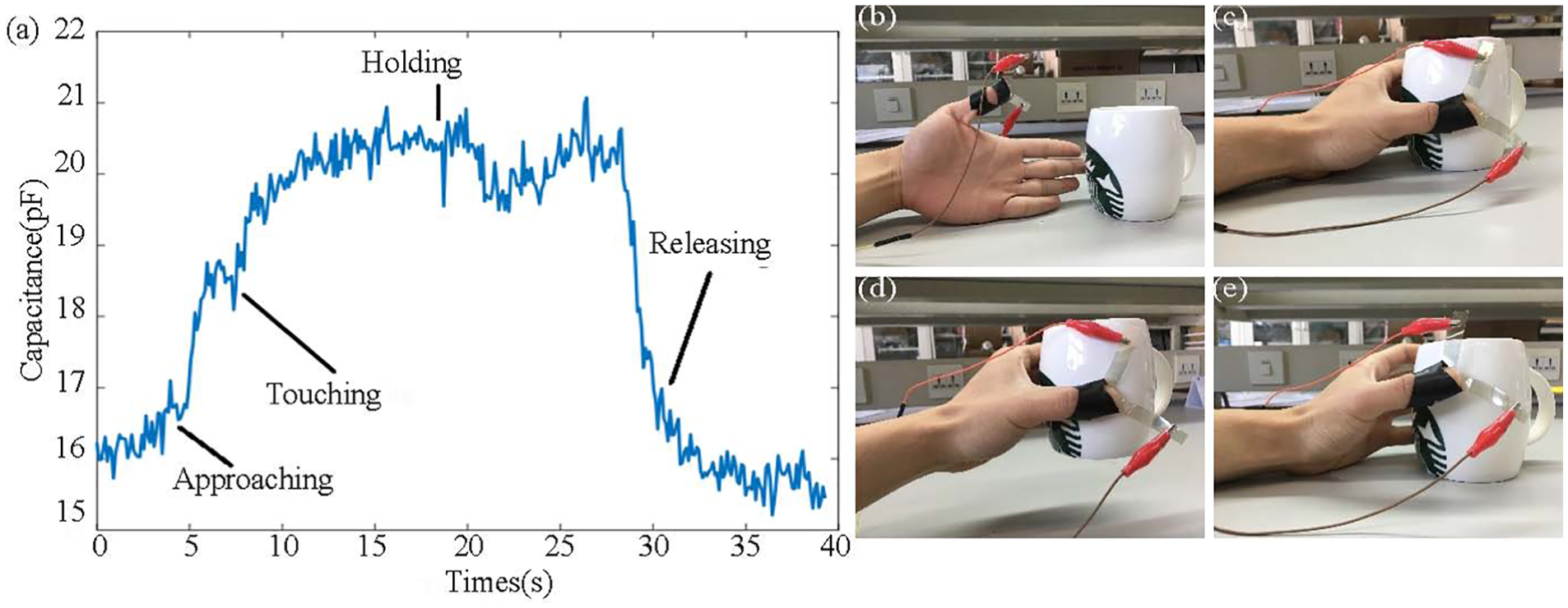
Pressure sensing of a human hand under different object manipulating motions (picking up and putting down a mug) with an e-skin sensing unit on the fingertip. The whole process (b) approaching, (c) touching, (d) holding, and (e) releasing could be clearly differentiated via (a) the capacitance variances
Conclusion
In summary, we investigated the pressure-sensing abilities of capacitive e-skin sensing units with dielectric layers of different microstructures theoretically and experimentally. We first proposed the mechanical models of capacitive e-skin sensing units with dielectric layers of flat, trapezoidal, half-cylinder, and pyramids microstructure and then validated these models using FEM simulations. It can be seen from the slopes of the pressure-electrode separation curves (kFlat =−0.1445 × 10⁻⁶, kTrapezoidal = −0.1566 × 10⁻⁶, kHalf-Cylinder=−0.1568 × 10⁻⁶, and kPyramids =−0.1881 × 10⁻⁶) that microstructures in the dielectric layer significantly improved the sensing abilities of the e-skin units. Among them, the e-skin sensing unit with micropyramids in the dielectric layer demonstrated the highest pressure-sensing sensitivity.
For the experimental studies, we fabricated e-skin sensing units with flat and micropyramids in the dielectric layer using a commercial precision abrasive sheet (268XA; 3M, Minnesota, MN, USA) as the mold and the PET/ITO films as the electrodes. Experimental results also proved that microstructure in the dielectric layer can significantly improve the pressure-sensing sensitivity of the e-skin sensing unit. There were differences between the simulation and experimental data. These could because that the relative dielectric constant of the e-skin sensing unit with microstructured dielectric layer changed with pressure due to the presence of air in the microstructure gaps, which was not considered in the simulations. Meanwhile, the nonlinear behaviors of the PDMS were ignored during the simulations for efficiency, which would also affect the results. These will be studied further in the future.
Despite of the simple structure of this sensing unit, it could be used as the auxiliary sensing unit of artificial prosthetics. We demonstrated its pressure-sensing ability by attaching it to a human fingertip and monitor human motions by recording the pressure changes. More work still needs to be done before it can be used in areas such as soft robots or artificial prostheses. For now, we have focused on sensing mechanism of an individual unit. In order to monitor deformations or interactions (by contact forces or pressures) of an entire soft robot or prostheses, a sensor network consisting of multiple pieces of individual sensing units is required. Sensing abilities of this network would be affected by the deformation and capacitance interferences among capacitors, which will be the next focus of our studies. Our further research also involves large-area e-skin fabrication, signal processing, human–machine interface, and so on.
Footnotes
Declaration of conflicting interests
The author(s) declared no potential conflicts of interest with respect to the research, authorship, and/or publication of this article.
Funding
This work was supported by the National Natural Science Foundation of China (grant nos 51705368 and 51605334), Natural Science Foundation of Shanghai (grant no. 17ZR1441800), and Shanghai Sailing Program (grant no. 17YF1420200).