
Abstract
Noise immunity is the foremost issue in high-speed domino circuits. In general, better noise immunity is achieved at the cost of speed and power degradation. In this paper, pseudo-dynamic keeper design is proposed to reduce the delay and power with improved noise immunity for domino circuits. The proposed technique is able to achieve reduced delay, power consumption, and better noise immunity by using always ON keeper. The simulation results show that the proposed technique exhibits 41%, 39%, and 19% delay reduction when compared with the low power dynamic circuit for two-input OR gate, two-input EX-OR gate, and 4:1 multiplexer. The proposed logic also performs better as compared to a low power dynamic circuit with 24%, 21%, and 14% reduction in power-delay product for two-input OR gate, two-input EX-OR gate, and four input MUX, respectively. The unity noise gain is also improved as compared to all other existing methods.
Introduction
Static CMOS logic circuits are good in noise immunity. However, the need for higher speed and lower power consumption has created interest to design dynamic logic circuits for the future generation of high-performance ICs. Domino logic is a widely used dynamic logic in high-speed VLSI architectures. The need of high fan-in domino gates has many applications in high-performance signal processing architectures such as DSP processors, programmable logic, and memories. 1 Domino logic-based circuits are almost four to five times faster than static CMOS logic circuits. Domino logic circuits frequently suffer from low noise margin and subthreshold leakage current. 2 Due to the low noise tolerance nature of dynamic domino circuits, the voltage in the dynamic node is easily affected by both external and internal noises. Noise in the dynamic logic circuits is defined as the deviation from the actual value of the signal stored.3–6 Noise sources in dynamic logic circuits are generally classified into two types: external noise and internal noise. External noise is usually caused by the coupling effect and neighboring channel crosstalk. These noises create serious problems in submicron VLSI circuits because of aggressive interconnect scaling. 3 Charge sharing and charge leakage are the primary causes for internal noises.7–11 Charge sharing usually happens during the evaluation phase of dynamic logic due to charge distribution in the adjacent dynamic nodes when the pull-down network transistors are “ON.” In general, a keeper circuit is used to diminish the effect of charge sharing and charge leakage. To accomplish better noise robustness, the keeper transistor must be upsized. The keeper ratio K is given by
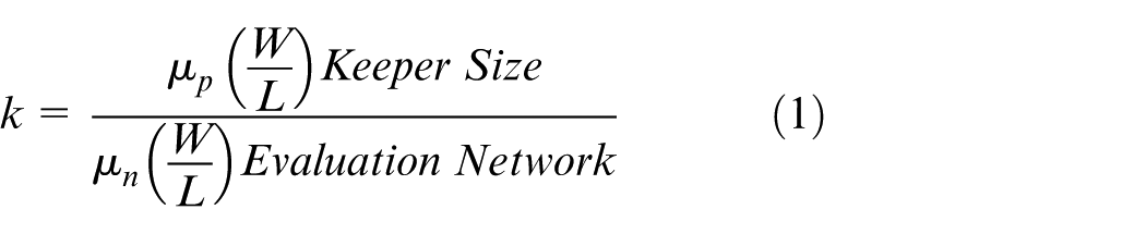
where µn is the electron mobility and µp is the hole mobility. Increasing the keeper size will improve the noise with increased power and delay due to the high contention current between keeper and pull-down network transistors. Normally, a trade-off can be maintained for speed, power, and noise robustness. 12 Hence keeper upsizing alone is not a feasible solution for high-performance noise-tolerant dynamic logic circuits. From the literature, numerous techniques have been proposed to improve noise immunity and performance of dynamic domino logic circuits. In the domino conventional keeper logic, the dynamic node is pre-charged through the weak keeper to VDD during pre-charge phase and the dynamic node maintains its value by this weak keeper transistor. This technique is less noise immune due to weak keeper transistor. In addition, the dynamic node tries to discharge the dynamic node voltage if the pull-down network is ON, in the evaluation phase. Meanwhile, the weak keeper tries to charge the dynamic node due to this action, the power and delay of the circuit will increase. High-speed domino (HSD) keeper 5 circuit is less noise tolerant due to floating nature of dynamic node during the commencement of evaluation phase.
The conditional keeper domino (CKD) 13 logic is good in noise robustness. But the power consumption and delay is increased due to the contention path between weak keeper and evaluation network. Due to the stacking effect of the diode footed domino (DFD) keeper 14 circuit, the evaluation delay is increased. The proposed logic in Asyaei 15 is less noise tolerant due to floating dynamic node in the evaluation phase. In general, except for the first stage, the evaluation network is OFF during pre-charge phase when the domino logic circuits are connected in a cascade manner. 16 There is contention current between the keeper and evaluation network transistors during the evaluation phase if the pull-down network is ON.
We propose a domino circuit with always ON strong keeper to reduce the delay of the domino circuits with improved noise robustness. The dynamic node is conditionally charged and discharged based on the pull-down network ON and OFF state. The following sections of the paper are organized as follows “Limitations of existing keeper–based domino circuits” discusses the existing keeper circuit limitations. In the section “Proposed pseudo-CMOS keeper,” we explain the proposed high-speed noise tolerant keeper circuit. The Section “Results and discussion” discusses results and discussions.
Limitations of existing keeper–based domino circuits
Conventional keeper
Figure 1 shows the conventional domino keeper circuit of a two-input OR gate. When clk = 0, the dynamic node (dyn) is pre-charged to VDD through the pull-up PMOS transistor. The dynamic node retains its value by using a weak keeper transistor MP1. Due to the weak keeper transistor, this technique is less noise tolerant. During evaluation, if the pull-down network is ON, the dynamic node tries to discharge its value through the pull-down network. At the same time, the keeper tries to charge the dynamic node and maintain its value as “1.” Due to this, there is degradation in power and delay in the circuit.
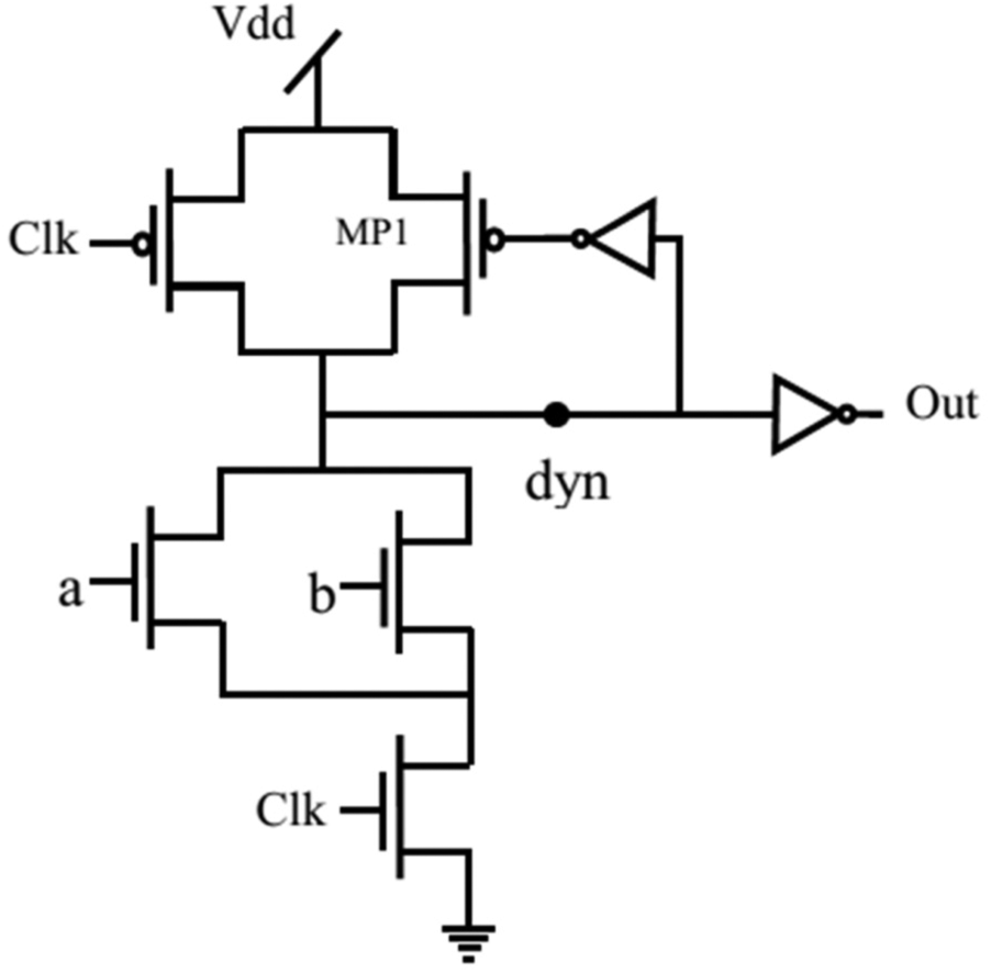
Conventional keeper.
HSD
Figure 2 shows the two-input OR gate with HSD keeper circuit. 5 When clk = 0, the dynamic node is pre-charged to VDD through PMOS MP1 transistor. Meanwhile, the gate of the MN1 transistor is triggered only by the previous clock, that is, “1” due to the delay of inverters and hence it passes logic “0” from the dynamic node to the gate of keeper transistor MP2 and turning it ON. By this way, the dynamic node holds logic “1” during the pre-charge phase. When clk = 0, after the delay of inverters, the gate of MP3 receives logic “0” which causes the keeper transistor to be in OFF state through the MP3 transistor. Thus, in the remaining portion of the period in pre-charge phase, the dynamic node will be floating. This results in reduction of noise robustness.
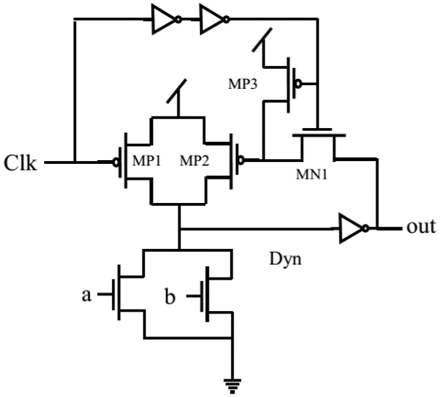
High-speed domino.
At the beginning of the evaluation period, the transistor MP2 is turned OFF. During this period, the dynamic node is again floating which also causes the circuit to be less noise tolerant.
Conditional keeper logic
Figure 3 shows the OR gate with two inputs using conditional keeper logic circuit. 13
Conditional keeper.
During the evaluation phase, if the evaluation network is OFF, the dynamic node holds logic “1.” This makes the NAND gate output to logic “0” after the two inverter delays and this turns ON the large keeper. The strong keeper will raise the noise immunity of domino logic circuits. However, the contention current between weak keeper and evaluation network transistors will increase the delay and power consumption.
DFD
Figure 4 shows the OR gate with two inputs using DFD logic. 14 Here, the stacking effect provided in evaluation network minimizes the leakage current. However, due to the height of the stack in the evaluation network, the evaluation delay is increased.
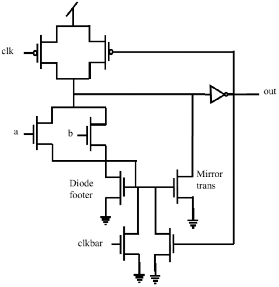
Diode footed domino.
The evaluation delay can be minimized by adding a current mirror transistor. However, the sizing of the mirror transistor will affect the noise immunity. Also, it is necessary to reduce the keeper transistor size to minimize the contention current between keeper and evaluation network.
Leakage current replica keeper
Figure 5 shows the OR gate with two inputs using leakage current replica (LCR) keeper. 17 In this keeper logic, the keeper strength is restricted by using the current mirror circuit. The LCR keeper performs well in the case of delay. However, this logic consumes high power, particularly for the higher input gates.
Leakage current replica (LCR) keeper.
Voltage comparison based domino keeper
Figure 6 shows OR gate with two inputs using a voltage comparison based domino (VCD). 18 In this logic, the output voltage is produced by using a sense amplifier. The sense amplifier compares the voltage across the pull-down network to produce the output. Here, the power consumption has decreased by reducing the switching capacitance voltage swing. The noise immunity of the logic can be increased by increasing the size of the mirror transistor. However, the delay and power consumption is increased.
Voltage comparison based keeper.
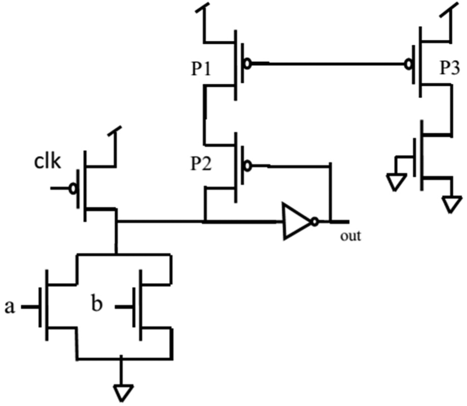
Low power dynamic logic keeper
Figure 7 shows the two-input OR gate with domino logic with complement CLK keeper 15 circuit. When clk = “0,” the dynamic node is pre-charged to VDD through the MP2 transistor. The MP1 transistor gate holds logic “0” which makes the transistor MP1 turn ON. Now, the “x1” node holds logic “1” and node “x2” holds logic value “0.” Thus, the transistor M2 is OFF and transistor M1 is ON. The dynamic node holds the logic “1” through the M1 transistor and MP1 transistor. When clk = “1,” if the evaluation network is OFF, the node x2 holds logic value “0” and the dynamic node retains its logic value as “1.”
Low power dynamic logic keeper.
If the pull-down network is ON, the node x2 will have logic “1.” The logic “1” in “x2” node turns OFF M1 transistor and turns ON M2 transistor to discharge the dynamic node. Here, the dynamic node is floating during the evaluation period which reduces the noise immunity of the circuit.
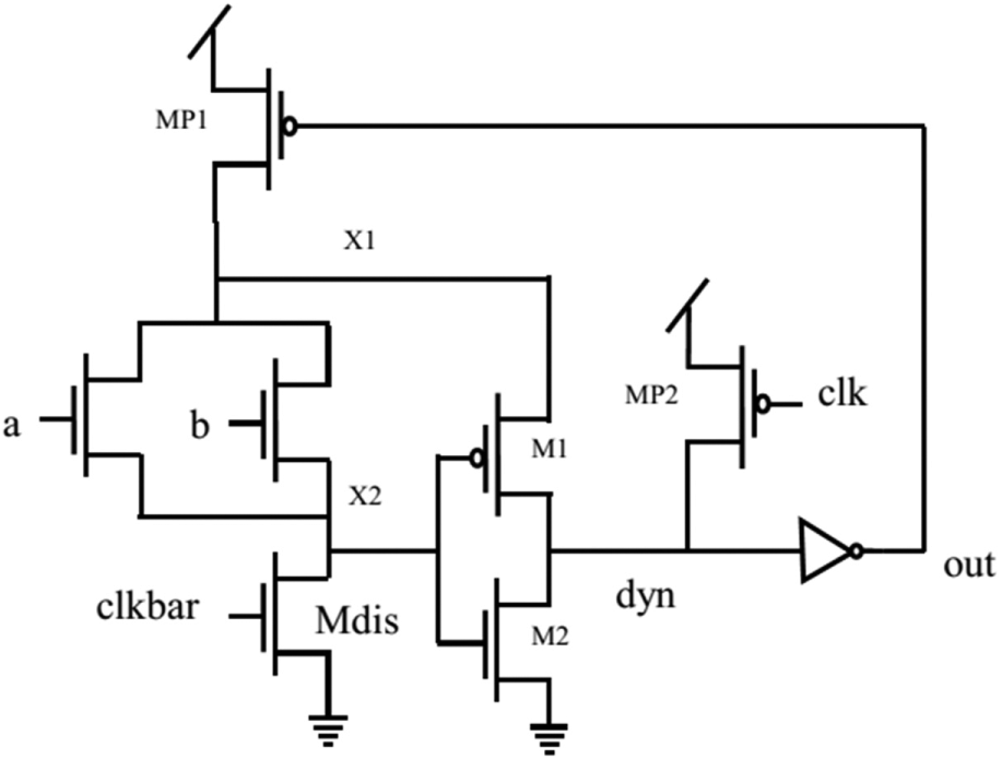
Proposed pseudo-CMOS keeper
Pre-charge phase
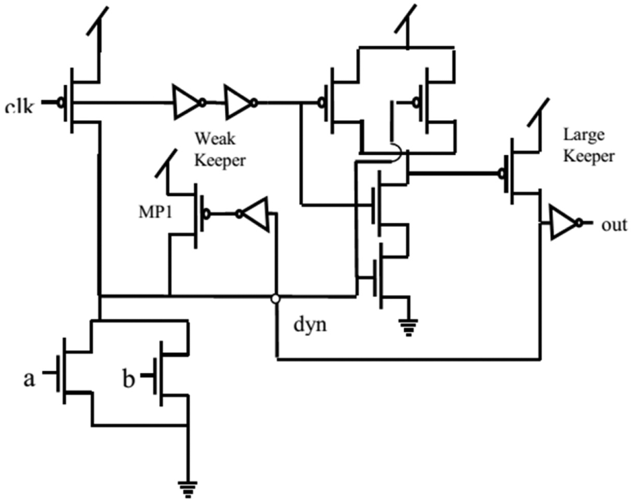
Figure 8 shows the proposed pseudo-CMOS keeper (PCK) circuit for a two-input OR gate. When clkbar = 1 (clk = “0”), the evaluation network is OFF. The node N1 is at logic “0” which turns ON the MP2 transistor and turns OFF the MN1 transistor. The dynamic node retains its logic “1” through MP2 transistor during its pre-charge phase.
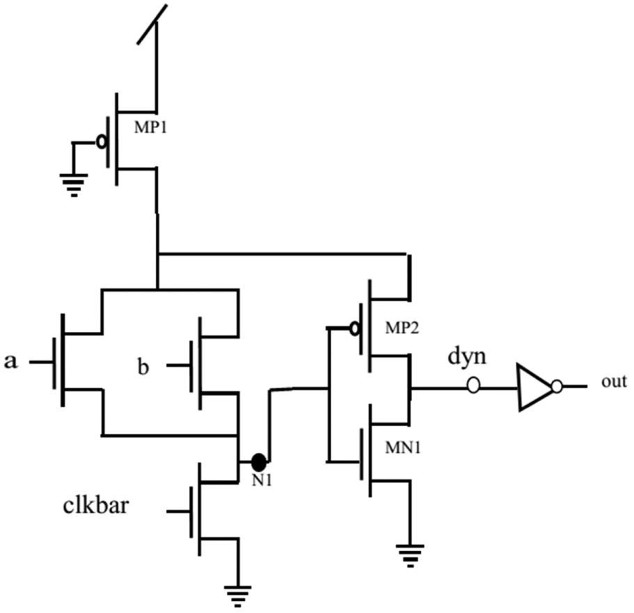
Pseudo-CMOS keeper (PCK).
Evaluation phase
When clkbar = “0” (clk = “1”), the footed transistor is OFF. If the evaluation network is OFF, then the node N1 holds logic “0” and the dynamic node keeps its high value through MP2. When clkbar = “0,” if the pull-down network is ON, then the node N1 holds logic “1” which turns OFF MP2 and turns ON MN1. The dynamic node voltage is discharged through the MN1 transistor. The transistor MP1 is always ON like pseudo-NMOS logic. The combination of transistors MP1, MP2, and MN1 almost behaves as a static CMOS inverter which is conditionally ON or OFF based on the node N1 logic value. Because of this static CMOS arrangement, the noise tolerance is increased.
Results and discussion
The simulations were done in HSPICE with 180 nm technology, VDD = 3.3 V, 110°C temperature, and 10 MHz clock frequency. The different keeper logics with OR gate circuits were simulated using HSPICE and compared with PCK. Table 1 shows the power-delay product comparison of two-input OR gate with different keeper logic circuits. From the table, we can observe that PCK has 44% reduced delay and power-delay product reduced by 32% as compared with conventional keeper logic for two-input OR gate.
Power-delay product comparison of different keeper logics for two-input OR gate.
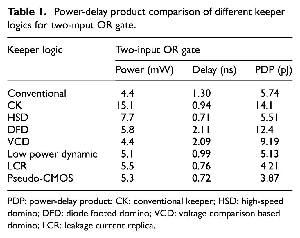
PDP: power-delay product; CK: conventional keeper; HSD: high-speed domino; DFD: diode footed domino; VCD: voltage comparison based domino; LCR: leakage current replica.
From Figure 9, we can observe that the delay of proposed logic is decreased as compared to all other existing keeper logics for two-input OR gate. The power-delay product comparison is shown in Figure 10. From the figure, we observe that the power-delay product is decreased for proposed logic as compared to all other existing logics. The simulation results show that the proposed logic has power-delay product for two input OR gates when compared with different keeper logic circuits such as conventional keeper logic, CKD, VCD, LCR keeper, DFD, HSD, and low power dynamic keeper circuit. 15 The improvement of the proposed PCK is evident from Table 1, Figure 9 and Figure 10. These wide fan-in gate designs with low power-delay product can be used in high-speed noise tolerant and low power applications.
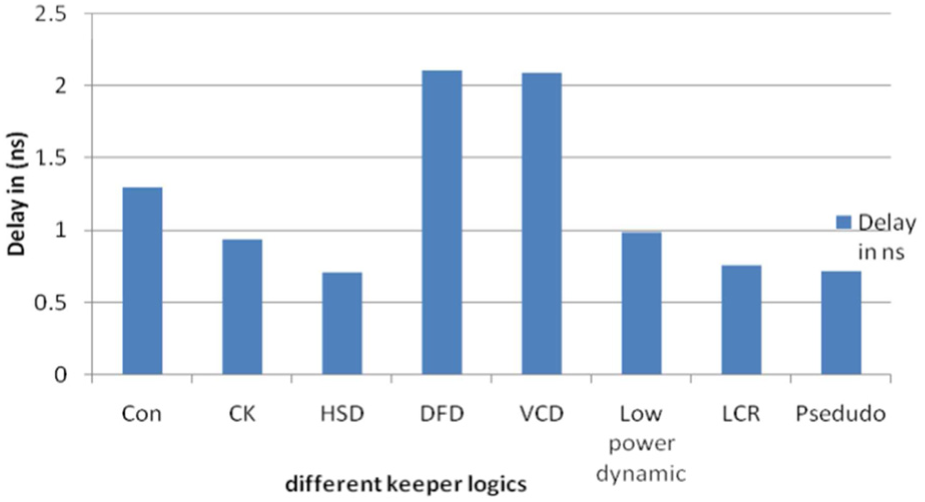
Graph for delay comparison of different keeper logics.
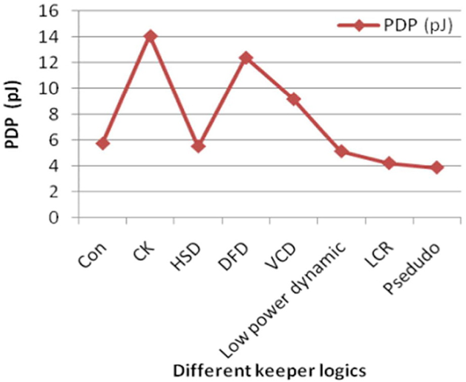
Graph for power-delay product comparison of different keeper logics.
Table 2 shows the power-delay product, unity noise gain (UNG) comparisons of two-input EX-OR gate and 4:1 MUX with low power dynamic keeper 15 and PCK logic. From the table, we can examine that the proposed PCK has a reduced power-delay product of 21% for two-input EX-OR gate and 14% power-delay product for 4:1 MUX as compared with the low power dynamic logic circuit (Figure 11). 15
Power-delay product, UNG comparison of XOR and MUX.
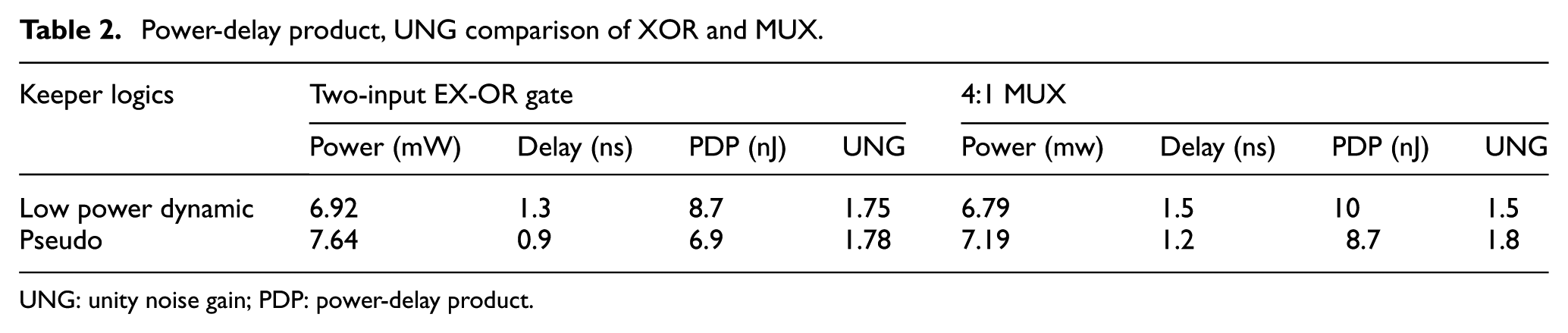
UNG: unity noise gain; PDP: power-delay product.
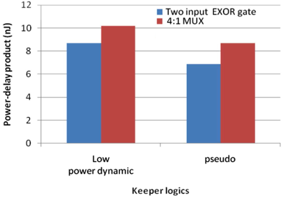
Graph for power-delay product comparison of different keeper logics for EX-OR and 4:1 MUX.
Transistor sizing
For a fair comparison, the width (W) and length (L) of evaluation network transistors are set as follows: Lmin = 180 nm and W = 3 L (540 nm), respectively. The PMOS to NMOS width of output inverter in all keeper circuits is set with the ratio 2:1. The required inverter delay for HSD and CK keeper has been achieved by increasing the length of the transistors.
Noise immunity
UNG is a commonly used parameter to evaluate the noise robustness of the dynamic circuit.18–22 The UNG is described as the value of noise amplitude at the input which produces the same noise amplitude at output.
15
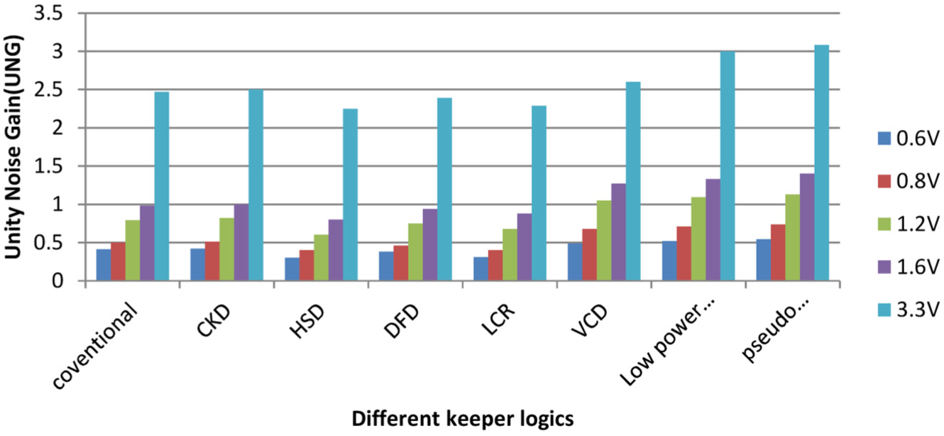
In this paper, the duration of the noise pulse is fixed as 3 ns and the amplitude of noise pulse is varied to find UNG. Table 3 shows the UNG comparison of two-input OR gate with PCK and all other existing logic for different operating voltages. From the table, we can examine that the proposed PCK has improved UNG of 18.4% as compared to the conventional keeper for two-input OR gate.
UNG comparison for different operating voltages for two-input OR gate.
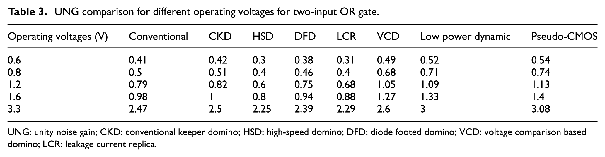
UNG: unity noise gain; CKD: conventional keeper domino; HSD: high-speed domino; DFD: diode footed domino; VCD: voltage comparison based domino; LCR: leakage current replica.
From Figure 12, we observe that the UNG is improved for proposed logic as compared to all other existing logics for two-input OR gate. It is evident that the proposed logic has improved noise immunity as compared to all other existing keeper logic techniques without compromising power-delay product. Table 4 shows the UNG comparison of two-input OR gate with PCK for different noise pulse duration. The operating voltage is fixed as 1.2 V for the above UNG comparison.
UNG comparison for different noise pulse duration.
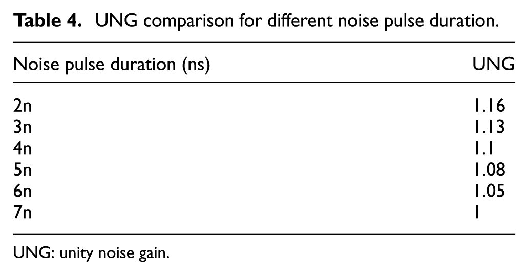
UNG: unity noise gain.
Graph for UNG comparison for different operating voltages.
From Figure 13, we can see that the proposed PCK has UNG that reduces linearly with increasing noise pulse duration. From Figure 14, we can see that the proposed keeper has reduced transistor count as compared to all other existing logics.
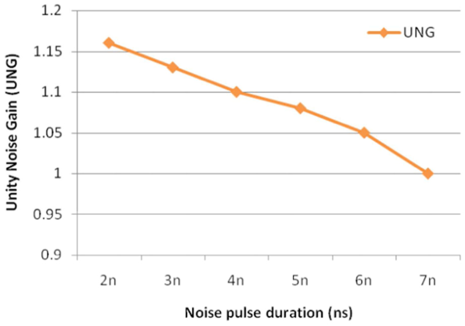
Graph for UNG comparison of pseudo-CMOS keeper for different noise pulse durations.
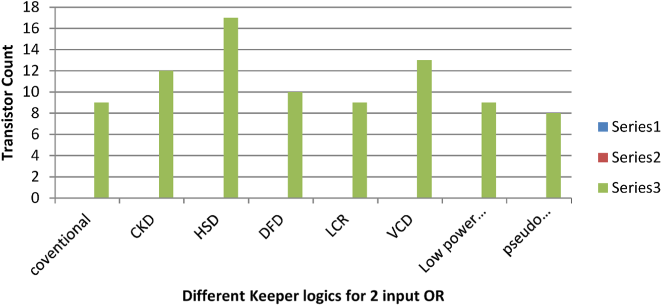
Transistor count comparison of two-input OR gate using different keeper logics.
Conclusion
Low noise invulnerability and the power consumption are the major problems in domino logic–based dynamic logic circuits. There is a trade-off maintained always between delay and noise immunity which affects the system performance. In this paper, PCK has been proposed to increase the speed with good improvement in noise robustness. The proposed logic has provided a low power-delay product and better noise robustness as compared to all other existing logics. The simulation results showed that the proposed keeper has reduced 41%, 39%, and 19% delay when compared with the low power dynamic CMOS logic circuit for two-input OR gate, two-input EX-OR gate, and 4:1 multiplexer respectively. The proposed logic also has reduced power-delay product with 24%, 21%, and 14% as compared to low power dynamic circuit for two-input OR gate, two-input EX-OR gate, and four input MUX, respectively. The proposed logic has also 18.4% of improved UNG as compared to the conventional keeper for two-input OR gate. The proposed logic requires less number of transistors as compared to all other existing logic without compromising delay.
Footnotes
Declaration of conflicting interests
The author(s) declared no potential conflicts of interest with respect to the research, authorship, and/or publication of this article.
Funding
The author(s) received no financial support for the research, authorship, and/or publication of this article.