
Abstract
The enhancement of Raman signals using photonic crystal structures has been the subject of numerous experimental and theoretical studies, leading to a variety of issues and inconsistencies. This paper presents a comprehensive experimental investigation into the impact of alignment between the laser excitation wavelength and the specific position of the photonic band gap on signal enhancement in Raman spectroscopy. By employing one-dimensional (1D) porous silicon photonic crystals, a systematic analysis across a large number of spectra was conducted. The study focused on examining the signal enhancement of both the Raman ∼520 cm–1 silicon band, representing the constituent material of photonic crystal, and the most prominent Raman bands of crystal violet, used as a probe molecule. The probe molecules were both infiltrated into and adsorbed on top of the photonic crystal structure. The obtained experimental results for the contribution of 1D photonic crystals to Raman signal enhancement are much smaller compared to most predictions. The Raman signal of silicon and the signal from the probe molecule are enhanced ≤2.5 times when the laser excitation aligns with the edge of the photonic band gap, strictly defined as the position at the very bottom of the reflectance peak. The results have been discussed within the context of theoretical explanations.
This is a visual representation of the abstract.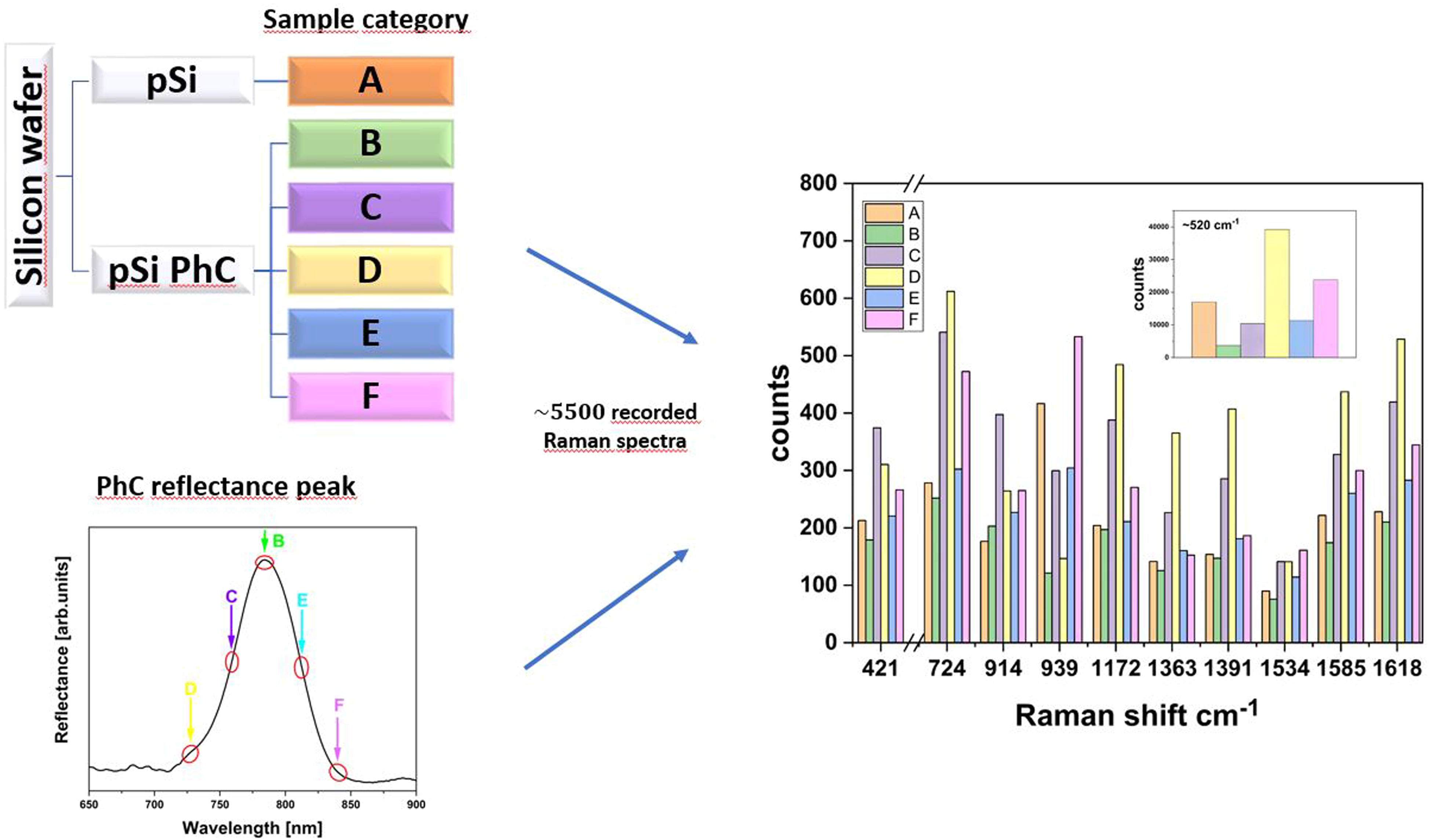
Introduction
Photonic crystals (PhCs) are a special class of periodically structured materials that possess translational symmetry in one, two, or three dimensions. 1 They have attracted significant interest in the last 35 years due to the possibility of effective control and manipulation of incoming electromagnetic (EM) waves.2–4 Whenever the periodicity of the dielectric constant is of the same order of magnitude as the wavelength of the probe light, PhCs exhibit a photonic band gap (PBG) where propagation of a certain light wavelength range is partially inhibited or even completely forbidden. 5 The PBG is a physical consequence of the multiple optical reflections at the interfaces of the layers that give rise to constructive interference and, thus, a photonic resonance feature with high reflectance. Another peculiarity of PhCs is local EM field enhancement that is closely connected to the anomalous group velocity dispersion at the edges of the PBG, 6 which results in a longer interaction time between light and material.7–9 Due to these unique properties, either as random porous or self-assembled periodical structures, PhCs have been utilized in a wide range of applications.10–12
Porous silicon (pSi), when produced by the electrochemical anodization of crystalline silicon (cSi) wafers, has shown to be a very suitable dielectric material for the formation of one-dimensional (1D) PhCs due to the simplicity of the etching process.13–15 The key observation for the successful production of pSi PhCs was that the already etched layer parts are unaffected by subsequent etching. Moreover, the temporal modulation of the etching current results in the corresponding changes in the substrate's porosity, which is in turn linearly connected with the refractive index. This fact enables the variation in the porosity-depth profile of pSi and allows the fabrication of any combination of layers with the required optical thicknesses. 16 Therefore, depending on the etching parameters and the programmed computer-controlled etch waveform, the desired optical properties of pSi PhCs can be adjusted to appear in the required spectral region. 17 Following the seminal reports from Vincent 18 and Berger et al., 19 many pSi multilayer systems have been experimentally reported and widely applied.20–22 Among these, very popular optical structures have been the rugate filters, with a continuous, sinusoidally varying refractive index distribution in the direction perpendicular to the filter plane. 23
Raman signal arises from inelastic scattering of photons with matter and due to the low probability for this scattering to occur, the corresponding signal is very weak. There have been numerous publications, both experimental and theoretical, that explore the phenomenon of Raman scattering enhancement by PhCs. However, the extensive review of the research that was conducted hitherto showed that there has been no systematic analysis of this topic and that the potential contribution of PhCs to the Raman signal enhancement is still unclear. The main issue in the literature is the position of the excitation laser wavelength relative to the PBG. Some authors have concluded that the highest enhancement factor (EF) can be attained when the laser excitation coincides with the center of the PBG (or when there is an overlap between Raman-shifted bands and PBG) due to the maximum backward reflection from the multilayer structure.24,25 Contrarily, various authors claim that the greatest signal enhancement occurs when the excitation is aligned with the edges of the PBG due to the decreased group velocity which produces longer light–matter interaction time, interpreted as increased local density of optical states.26–29 Moreover, there are reports that either define differently the edge of the PBG or do not provide enough details about the relative position between the excitation and PBG.24,30–32 Another inconsistency evident in the literature pertains to the enhancement EF that ranges from two31,33,34 to 102–103.26,30,35 Additionally, there is an ambiguity regarding the possible enhancement of the optical near-field both inside and outside PhCs, i.e., reports of the Raman signal enhancement from material that composes the investigated structure24,26,27,34–42 and reports that used Raman signal enhancement from molecules either injected into or attached on the surface of PhCs.25,28,30–32,41 The other issues and contradictory findings include the different influences of 1D, two-dimensional (2D), and three-dimensional (3D) PhCs, different reported magnitudes of maximum reflectance corresponding to PBGs or even their complete indefinability, and especially the usage of only one Raman band or only a few Raman spectra when defining signal enhancement. It is important to emphasize that the same dubieties are also present in articles that exploit both PhCs and the surface-enhanced Raman spectroscopy (SERS) effect for Raman signal enhancement, but the synergy of photonics and plasmonics will not be covered in the present paper. For clarity, Table I presents and summarizes the aforementioned issues.
A summary of previous explorations on Raman signal enhancement by photonic crystals.
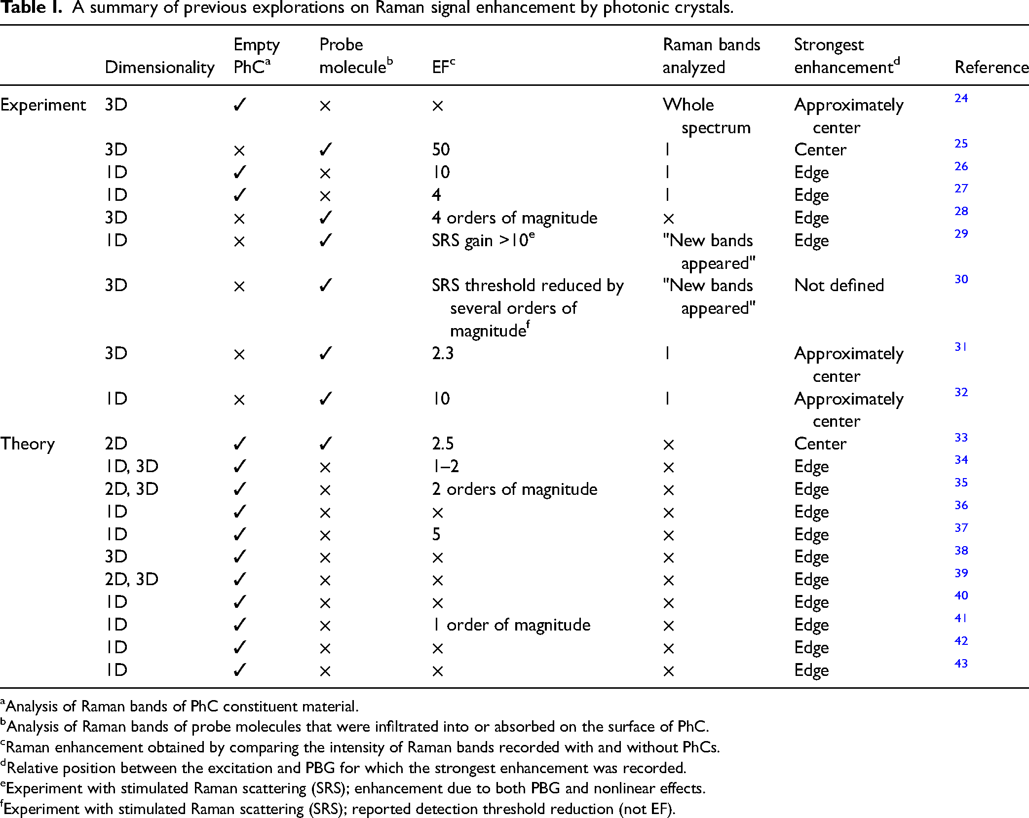
Analysis of Raman bands of PhC constituent material.
Analysis of Raman bands of probe molecules that were infiltrated into or absorbed on the surface of PhC.
Raman enhancement obtained by comparing the intensity of Raman bands recorded with and without PhCs.
Relative position between the excitation and PBG for which the strongest enhancement was recorded.
Experiment with stimulated Raman scattering (SRS); enhancement due to both PBG and nonlinear effects.
Experiment with stimulated Raman scattering (SRS); reported detection threshold reduction (not EF).
In this contribution, we have used 1D pSi PhC and experimentally on a large number of spectra investigated the effect of alignment between the laser excitation wavelength and the specific position of the PBG on the signal enhancement of both the Raman 520 cm–1 silicon band and the most pronounced Raman bands of a probe molecule crystal violet (CV).
Materials and Methods
Preparation of pSi PhCs
Porous silicon (pSi) PhC samples were prepared using p-type boron-doped silicon wafers with resistivity 0.005 Ω·cm, crystal orientation 〈100〉, and thickness 525 ± 20 µm (Siegert Water GmbH). Before etching, silicon wafers were first cut to ∼2 × 2 cm2 squares, and a sacrificial porous layer was removed 17 using a homemade Teflon electrochemically etched cell with a piece of aluminum foil as a back-contact. Platinum mesh, as a counter-electrode, was suspended at a fixed height above the silicon wafer. Removal of a sacrificial layer was conducted in a 3 : 1 mixture of 40 wt% hydrogen fluoride (HF) and 99.8% v/v ethanol using a computer-controlled (LabView, National Instruments) programmable current source (2601B SourceMeter, Keithley Instruments Inc.) with a constant current density of 175 mA/cm2 applied for 30 s. The HF solution was then removed, and the cell was filled with 1 M potassium hydroxide (KOH) aqueous solution causing the dissolution of the porous layer. Following a 5 min interval, the KOH solution was extracted from the cell, and a wafer was thoroughly rinsed in ethanol. The same 3 : 1 HF–ethanol solution was used for the preparation of pSi and pSi PhC samples. pSi samples (sample category A) were etched by applying a constant current density of 25.5 mA/cm2 for 250 s, while pSi PhCs (sample categories B, C, D, E, and F) underwent etching with a sinusoidally modulated current density from 1 to 50 mA/cm2, applied and repeated for 50 cycles. The sinusoidal current profile period was altered from 4.386 to 4.95 s to create different specific positions of the pSi PhC reflectance peaks relative to the incident laser excitation. Finally, all samples were rinsed twice in ethanol and dried with a gentle stream of nitrogen gas. The etching procedure was done in a well-lit room at a fixed temperature T = (22.0 ± 0.1) °C. Four samples were etched for each sample category (A1, A2, A3, A4, B1, …, F4), i.e., 24 samples in total were made. Then, each sample was cut into small pieces, and three rectangles (i.e., A1-1, A1-2, A1-3, A2-1, A2-2, A2-3, etc.) belonging to the very center of the etched area where the applied current density is the most uniform, 44 with approximate dimensions of 2 × 3 mm2, were used for Raman measurements, making a total of 72 rectangular specimens.
Characterization of Samples
Details about the position and the width of PBGs, as well as maximum reflectance, were obtained using an ultraviolet–visible–near-infrared (UV-Vis-NIR) Shimadzu UV-3600 spectrometer (Shimadzu Corporation). Spectra were recorded in the reflectance mode over the 400–1300 nm spectral range, with a resolution of 1 nm and aperture of ∼13 nm. The angle of incidence for the reflectance measurements was 7°. The morphology and thickness of the prepared pSi and pSi PhC structures were examined using a Jeol JSM-7000F (Jeol Ltd) thermal field-emission scanning electron microscopy (FE-SEM), operating in the range of 5–15 kV, coupled with energy-dispersive X-ray spectroscopy (EDX).
Raman Measurements
To remove the surface oxide layer, each rectangular sample was immersed in 2 wt% HF solution for 30 s, followed by rinsing two times in ethanol and air-drying. Dried samples were then put into 0.5 mL of 10–2 M CV, prepared by dissolving CV powder in Milli-Q water, and left in the solution for 90 min. At the end of the incubation time, the CV solution was pipetted out and rectangular samples were placed upwards on clean paper and left to dry in the air.
Unpolarized NIR 785 nm laser excitation (InVia Raman microscope, Renishaw PLC) with a Leica ×10 N PLAN objective (numerical aperture 0.25) was used for Raman measurements. At the beginning of each experiment, the spectrometer was calibrated with an internal cSi(110) sample measured at 520.5 cm–1. Then, to avoid intensity differences of transverse-optical phonon scattering at the center of the Brillouin zone of 〈100〉 cSi (and pSi), due to in-plane orientation,45,46 the angular position of every rectangular specimen was fixed to provide the strongest Raman signal. The Raman spectra were acquired from three different, randomly chosen positions on every rectangular specimen, with 24–25 spectra recorded at each mapping area. The step size was fixed at 20 µm so the average surface area covered during each Raman measurement was ∼0.01 mm2. The laser spot diameter was ∼8 µm and the laser power was set to 10% (∼3 mW). The integration time was 1 s with five accumulations. All spectra were recorded in a spectral range between 350 and 1700 cm–1. For clarity, the schematic given in Figure 1 explains the branching for sample category A, while the complete view for the whole experiment is given in Figure S1 (Supplemental Material). The software Kinetics, running under Matlab R2010b (The Mathworks Inc.) was used for baseline correction of spectra, and Gaussian fitting with fixed CV peak center positions was performed in Origin (OriginLab Corporation). The exact average values and standard deviations for each sample category were calculated in Matlab R2010b (The Mathworks Inc.).
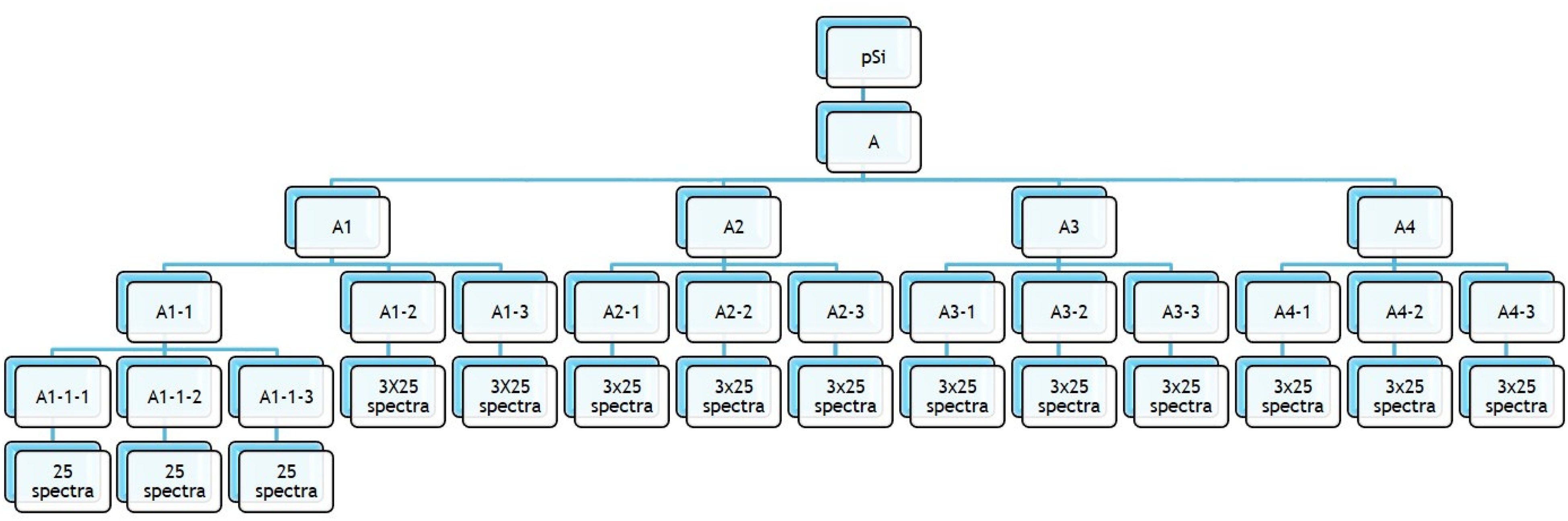
Schematic view of sample category A division into four samples (from A1 to A4), 12 rectangular specimens (from A1-1 to A4-3), three randomly chosen positions on each rectangular specimen (from A1-1-1 to A4-3-3), and ∼25 recorded Raman spectra for each mapping area.
Results and Discussion
As briefly explained in the introduction, both ambiguities and inconsistencies are present in the literature regarding the overlap combination of the laser excitation wavelength and the specific position in the PhC stopband which provides the greatest Raman enhancement. Foremost, we should distinguish between the two possible Raman signals that might be enhanced, e.g., the Raman signal of the material from which PhC was made and the Raman signals of probe molecules. Additionally, the signal of probe molecules can come from the interior of PhC or its surface, depending on whether the molecules can infiltrate the interior or be attached to the surface of PhC. In our experiment, the emphasis was placed on Raman signals from molecules and their possible enhancement due to the unique properties of PhCs. On the other hand, the Raman signal of silicon, aside from determining its possible enhancement, served as an additional validation for matching of laser wavelength with a specific position in the PhC PBG. For that purpose, the excitation laser wavelength had to be carefully chosen. Previously, our group used NIR 1064 nm laser and metal-coated pSi PhC as SERS substrates, but, due to the induced photoluminescence of cSi when using ordinary pSi, there was no way to quantitatively stipulate the potential contribution of PhC to the SERS signal enhancement.47,48 In this work, a 785 nm laser was utilized because of the three crucial advantages: (i) the detector's high recording speed, being an absolute necessity when obtaining a huge amount of Raman spectra for statistical purposes, (ii) the absence of fluorescence emission and low absorption of nanoporous silicon at this wavelength, and (iii) the nondestructiveness of this particular wavelength for future measurements of fragile biomolecules. The second fact enabled a ∼10 μm laser light penetration49,50 through a pSi layer to the cSi substrate. The Raman spectra of both pSi and cSi possess a transversal optical phonon band at ∼520 cm–1, although its intensity (if every parameter such as wafer doping, and orientation is held constant) is stronger in cSi.
Characterization of Samples
Ultraviolet–Visible–Near-Infrared (UV-Vis-NIR)
From the available literature, it is not clear whether the strongest Raman signal enhancement is achieved when the incident laser excitation overlaps with the center of the PBG or its edge. Furthermore, the PBG edge is not unequivocally determined since some authors defined it as the minimum of the reflectance peak and others as a position at its half maximum. Moreover, there is a difference between the low- and high-frequency sides of the PBG. 51 In this work, apart from ordinary pSi (sample category A), which was used as a standard, we systematically examined all these cases using five different relative positions between the laser excitation and the PBG (shown in Figure 2a). Position B corresponds to the case where the incident excitation coincides with the center of the PBG, and positions C and E correspond to the case when the laser matches ∼50% of the reflectance peak on the high- and low-frequency side, respectively. Finally, positions D and F serve to examine signal enhancement when the excitation coincides with the minimum reflectance on the high- and low-frequency side of the PBG, respectively. For the abovementioned reasons, we decided to perform extensive research on a large number of spectra and statistically analyze the enhancement of both the Raman peak of silicon and the most pronounced CV bands.
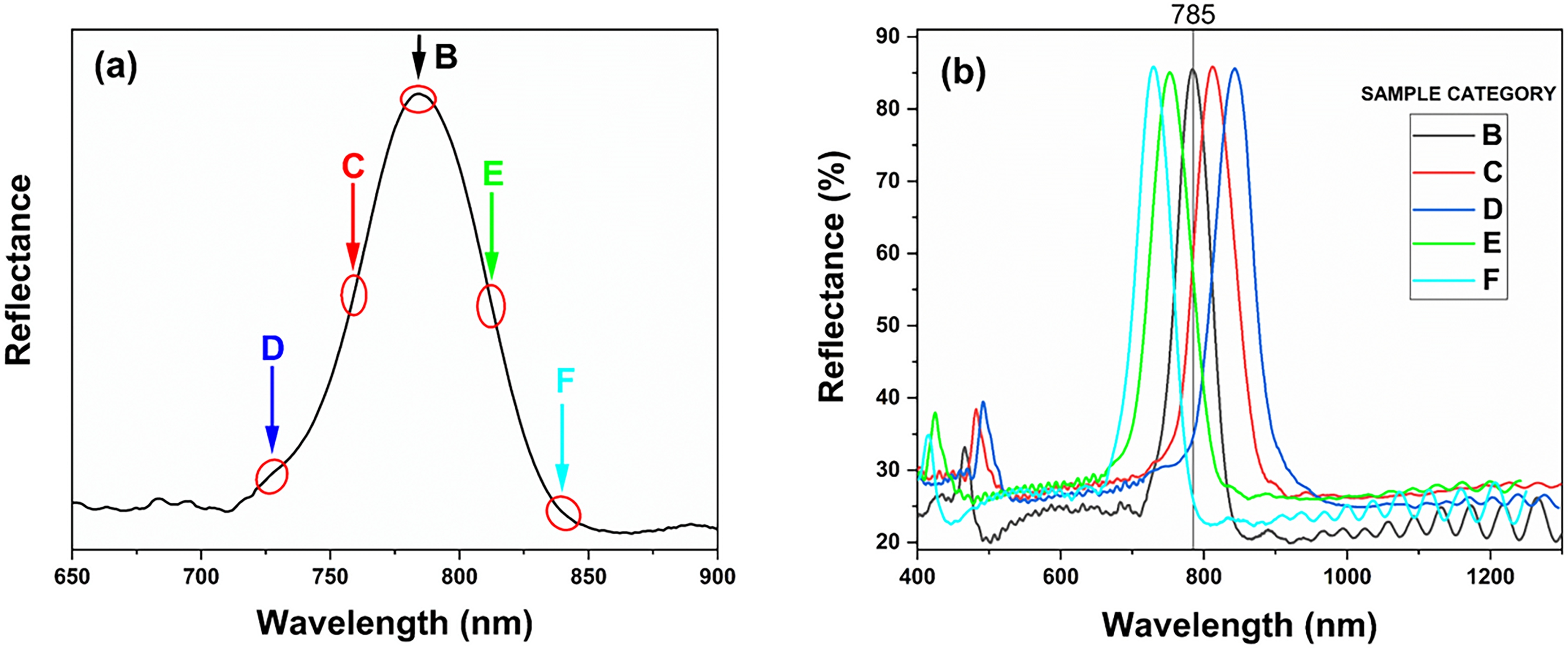
(a) Five different positions of alignment (representing five sample categories B–F) between the laser excitation and the reflectance peak of a rugate filter. (b) Reflectance spectra of pSi PhC representing five sample categories (B–F). Samples were prepared using the same sinusoidal current densities and the same number of different periods. The vertical line indicates the 785 nm laser excitation.
In this study, highly doped p-type cSi wafers were used for producing pSi PhCs since they permit the widest range variation of the fabrication parameters. 52 As a consequence, a PBG with a predefined width can be easily tailored to appear in the required spectral region. To probe both ends of the PBG for possible Raman signal enhancement, the photonic structure of choice was the rugate filter. 53 This structure, although rather uncommon compared to the usually employed Bragg reflector, can have an extremely narrow PBG, 54 and this fact served as a key benefit for our case. Thus, with the appropriate, fixed selection of etching parameters, the position of the PBG center can be gradually shifted relative to the excitation laser wavelength just by changing the period of the sinusoidal etching current. 55 It is important to mention that another (definitely easier) method to shift the position of PBG is to vary the incoming light angle of incidence. 55 Unfortunately, our Raman equipment does not have the option to tilt either the specimen or the laser. Therefore, in our experiment, the etch period was varied and the stopband positions of the produced pSi PhC are shown by reflectance spectra, recorded in specular geometry (Figure 2b). The main idea behind Figure 2b is to display our capability to produce samples where the excitation laser wavelength is aligned with the aforementioned specific positions (B–F) in the PBG. The spectra consist of sharp reflection resonances corresponding to the principal stopbands of a rugate filter, weaker second-order stopbands at approximately twice the shorter wavelength, very low reflectance elsewhere, and Fabry–Perot interference fringes at higher wavelengths. The reflectance peak wavelength shift was about 115 nm toward the higher wavelengths with the increase of the etching period from 4.386 to 4.95 s. The maximum reflectance reached a value of around 85% (with unavailability to increase it further, as described elsewhere47,48) and the full width half-maximums (FWHMs) of the stopbands remained almost constant indicating uniform optical thickness throughout the PhCs. The Bragg attenuation length for the maximum reflectance56,57 was calculated to approximately be slightly less than 3 μm. The reflectance of ordinary pSi (not included in Figure 2b) has an almost constant value of ∼20–25% throughout the spectrum but starts to rise in the low-wavelength region (<450 nm). The reflectance spectra were measured at 7° incidence, meaning that the actual position of each reflectance peak is shifted toward higher wavelengths by factor cos(7°).58,59 Also, the presented reflectance measurements were performed immediately after sample fabrication to prevent any oxidation. On the other hand, the recording of Raman spectra was not done on the same day hence the pSi PhC samples had to be dipped in a low concentration of HF solution to remove native oxides on surfaces before any kind of sample preparation for measurement. This dip led to a small but noticeable blueshift of the reflectance peak; for instance, 30 s dip in 2 wt% HF decreases the reflectance peak wavelength by 2–3 nm. This blueshift is, apart from the substitution of oxygen with fluorine atoms in the creation of dangling bonds, mostly due to the effect of chemical etching—a minute increase in porosity of the whole etched porous layer and, consequently, a slightly lower refractive index which shifts the position of reflectance peaks to slightly lower wavelengths. 17 Finally, sample incubation in a solution with a high concentration of CV (and subsequent air-drying) leads to the visible adsorption of probe molecules on the surface of PhC and possible infiltration inside the PhC. This coating is responsible for a blueshift of the stopband center by ∼15 nm and a decrease in the peak reflectance by ∼3%. The width of the PBG after immersion did not change indicating preserved uniformity over the sample in terms of optical reflectance. In addition, the blueshift due to the CV coating implies that the dominant contribution to the reflection peak position comes from the newly formed layer of molecules adsorbed on the surface and that the possible increase of the effective refractive index of PhC by infiltrated molecules is a minor effect. Therefore, to ensure the precise overlap of the excitation wavelength with the specific position in the PBG, all these corrections, transparently summarized in Table II, have to be taken into consideration when adjusting the period of sinusoidal etch current density. Also, it is important to mention that, since the FWHM of the reflectance feature for our samples was ∼45 nm, a small deviation from a certain position (>7–10 nm) drastically changes the relative position between the incident radiation and the PBG. For that reason, only small uncertainty wavelength intervals of ±2 nm around each predefined position, belonging to sample categories B to F, were allowed. In our experience, the room temperature during the etching process and the incubation had a strong influence on the reflectance peak position for our samples, 48 so it had to be carefully maintained at a fixed value.
Experimental corrections for the reflectance peak position/example for peak initially measured at 785 nm.
Field-Emission Scanning Electron Microscopy (FE-SEM) and EDX
The morphology of the porous surface was examined by scanning electron microscopy. Figure 3a shows the high-magnification top-view FE-SEM image of pSi PhC samples. The image reveals a typical mesoporous morphology, usually obtained when etching highly doped p-type cSi, with pore diameters of ∼10–20 nm. Noteworthy, due to the same average etching current density, the top surfaces of all samples (pSi and all pSi PhCs) have practically identical morphology. 17 The cross-sectional view (Figure 3b) presents the validation of the programmed etch structure with the obvious smooth variations of the rugate's filter high and low porosity layers perpendicular to the plane of the filter. A periodic pattern, designed for the stopband peak around 785 nm, is maintained over the whole etched layer which consists of 50 periods and the overall porous thickness is ∼7.5 μm. Figure 3c depicts a low-magnification scanning electron microscopy (SEM) image of a porous surface after 90 min of incubation in a 10–2 M CV aqueous solution. This image shows that the top surface is completely covered with continuous CV film blocking the pores and it was not possible to obtain any clear image in higher magnification. The high concentration of probe molecules was shown to be optimal to counteract the weak Raman signal and to produce a sufficient signal-to-noise ratio. The cross-sectional view of the incubated sample looked visually the same as the as-etched sample, i.e., it was not possible to visually determine if the CV molecules diffused into the porous structure. For this reason, we used EDX which revealed the difference in cross-sectional elemental compositions of as-etched and incubated pSi PhC samples (Figure 4). The presented EDX measurements covered approximately the same sample depth (<3 μm), shown by yellow circles in both images. From the inset tables in Figures 4a and 4b, it is obvious that the number of carbon atoms, being the major constituent of CV molecules, increased ∼2.5 times in the case of incubated sample, indicating an infiltration of molecule inside the structure. It is important to emphasize that the carbon tape, used to stick the samples to the SEM holder, was at least ∼500 μm farther and could not interfere with the measurements. The 1% of fluorine atoms visible in the case of the as-etched sample are probably remains from the etching procedure and the 1% of chlorine atoms in the case of the incubated sample definitely belong to the CV molecule. On the other hand, the approximately four times increase in oxygen atoms, although not easily explained, might have come from the fast oxidation of the incubated sample's cross-section, since this particular sample was left outside of the SEM chamber during the recording of the as-etched sample. Nevertheless, the most important result divulged by the EDX is the verification of the CV molecules penetration of the PhC, i.e., the molecules are not confined only to the PhC surface. This result was expected since the average pore size is more than 10 times larger than the CV molecule reported molecular size of 1.4 × 1.4 nm. 60 We also found that the CV molecules diffused into slightly less than half the thickness of the porous layer since the elemental composition of the incubated sample layers deeper than ∼3.5 μm was the same as the one from the as-etched sample (not shown).
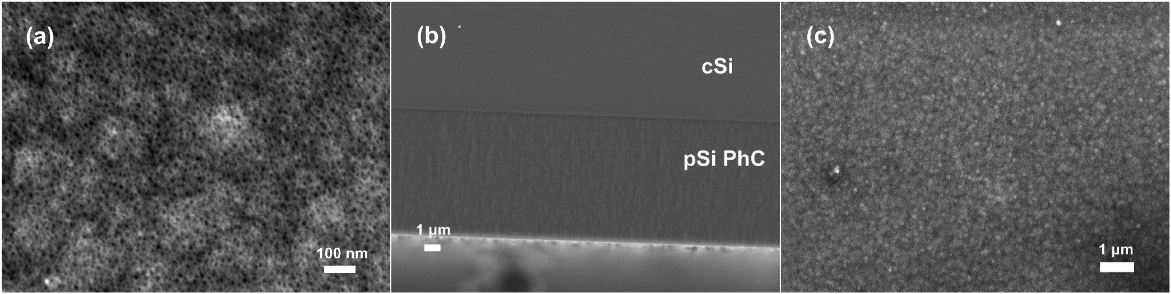
Field-emission scanning electron microscopy (FE-SEM) images of a pSi PhC sample. (a) Top-view image of the as-etched sample showing the pores on the surface. (b) Cross-section image of the as-etched sample showing the whole rugate structure. (c) Top-view image of the sample incubated in 10–2 M CV with continuous CV film over the pores.
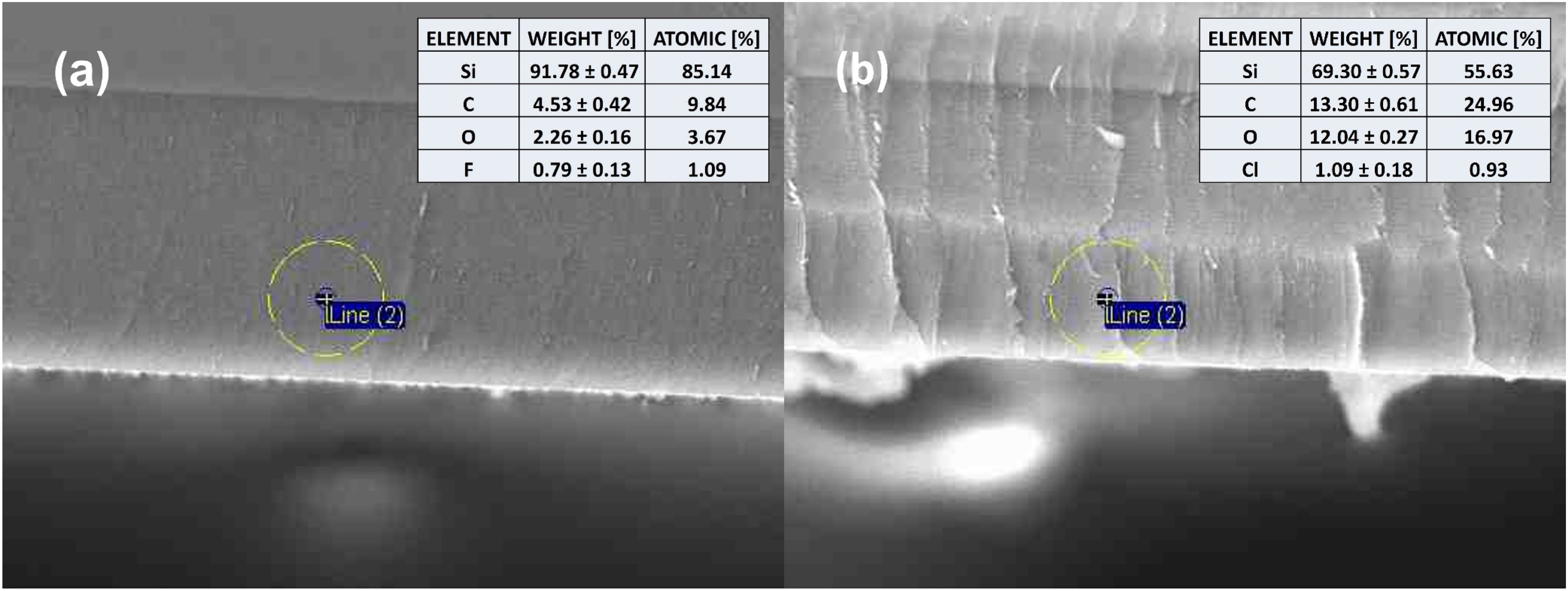
Field-emission scanning electron microscopy (FE-SEM) cross-section images with corresponding EDX elemental analysis of (a) as-etched pSi PhC sample and (b) pSi PhC sample incubated in 10–2 M CV.
Raman Measurements
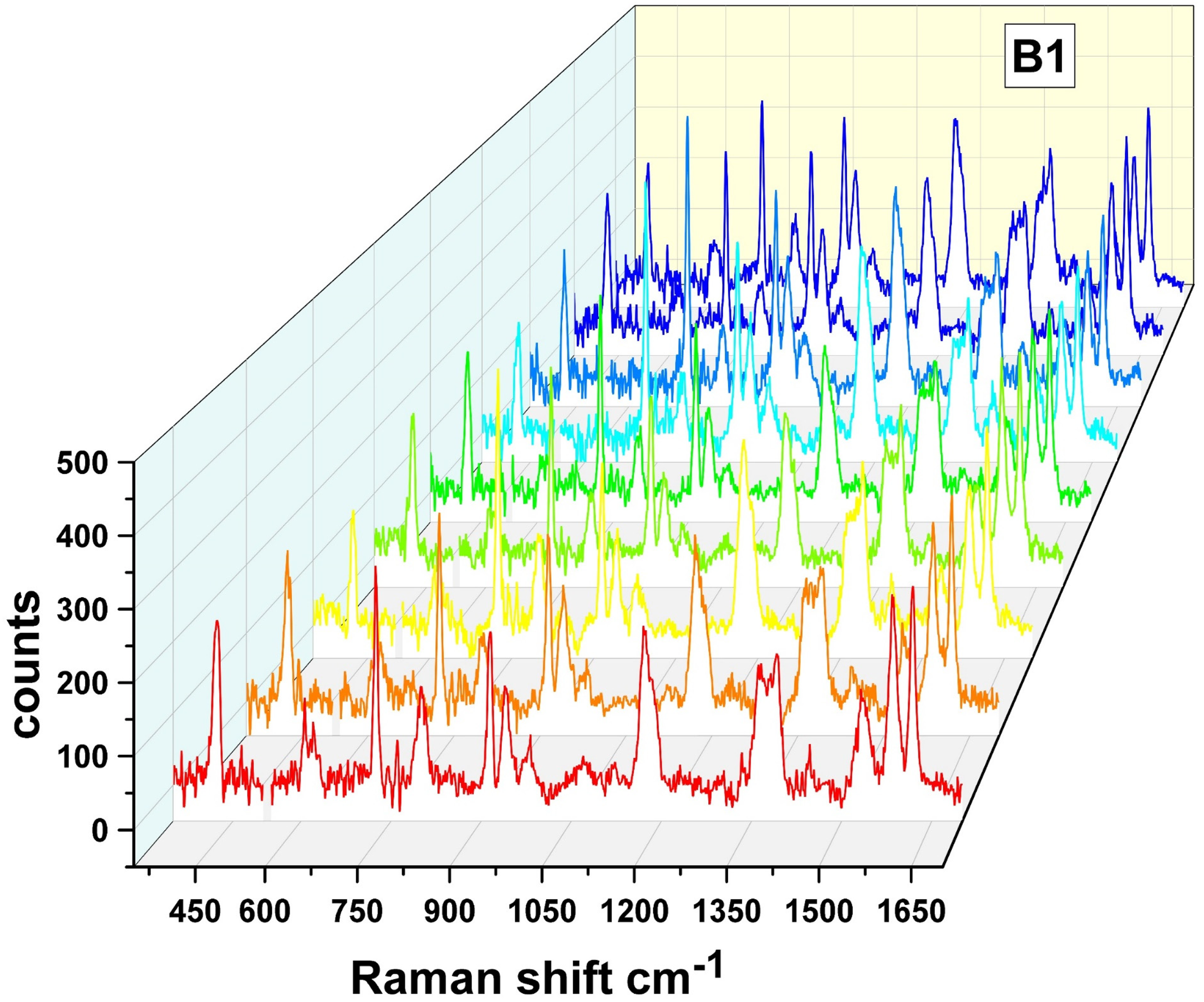
Raman spectra were obtained using 785 nm laser excitation and 24–25 spectra were recorded on every mapping area. The difference in the number of recorded spectra was a consequence of experimental setup constraints, in which only the mapping area and the step size could be defined, but not the number of spectra. It is important to mention that some sets of spectra, recorded in one mapping area, contained one or two outliers whose Raman signal was either much stronger or much weaker in comparison to other spectra, and Figure 5a presents one such data set in a waterfall. The Raman signal of silicon at ∼520 cm–1, representing the material from which PhC is made, is rather uniform, and the outlier corresponds to the Raman signal from the CV molecule. Actually, the outliers predominantly originated from the Raman signal of our probe molecule. Regarding the few outliers concerning the intensity of silicon ∼520 cm–1 peak, they can be explained as follows. The use of aluminum backside contact with the silicon wafer usually leads to homogeneous PhC layers in the middle of the wafer. Since the reflectance spectra shown in Figure 2b (with narrow FWHMs of reflectance peaks) are a macroscopic feature (recorded on an area >40π mm2), while the Raman laser spot size was much less than 20π μm2, the ∼520 cm–1 band outliers were probably due to the minute inhomogeneities of the local electric field during etching. These inhomogeneities produced the local change in the rugate's filter effective index of refraction and, therefore, affected and changed the defined sample category. This claim is confirmed by observing the spectra from sample category A, representing ordinary pSi, where there are no outliers regarding the ∼520 cm–1 peak. Within a particular sample category, as will be discussed, there was a <15% standard deviation from the mean intensity of a ∼520 cm–1 peak. On the other hand, the outliers concerning the intensity of the CV peaks probably came from the local (de)accumulations of CV molecules, both inside and on the sample surface, due to the imperfection of the incubation method. An optical image recorded by a Raman microscope showing the typical rectangular specimen coated with CV molecules is given in Figure 5b. The white rectangle represents the randomly chosen mapping area and localized aggregations of CV molecules, visible as black spots, can be seen throughout the surface. As there was <25% spot-to-spot intensity variation across all CV Raman bands, for more than 90% of spectra over every mapping area recorded, it can be inferred that the quasi-uniform coating by molecules was achieved. One of the issues in quantizing Raman enhancement by PhCs mentioned in the introduction was that the majority of previous studies reported results based only on a few spectra, and some of the reported enhancements possibly resulted from the outliers, i.e., spectra with the unrepresentative Raman signal. Consequently, for a pertinent scientific paper regarding this topic, an extensive statistical approach is needed and, in our opinion, any study containing only a few spectra should not be taken as the corroboration of the PhC influence on the Raman signal enhancement.
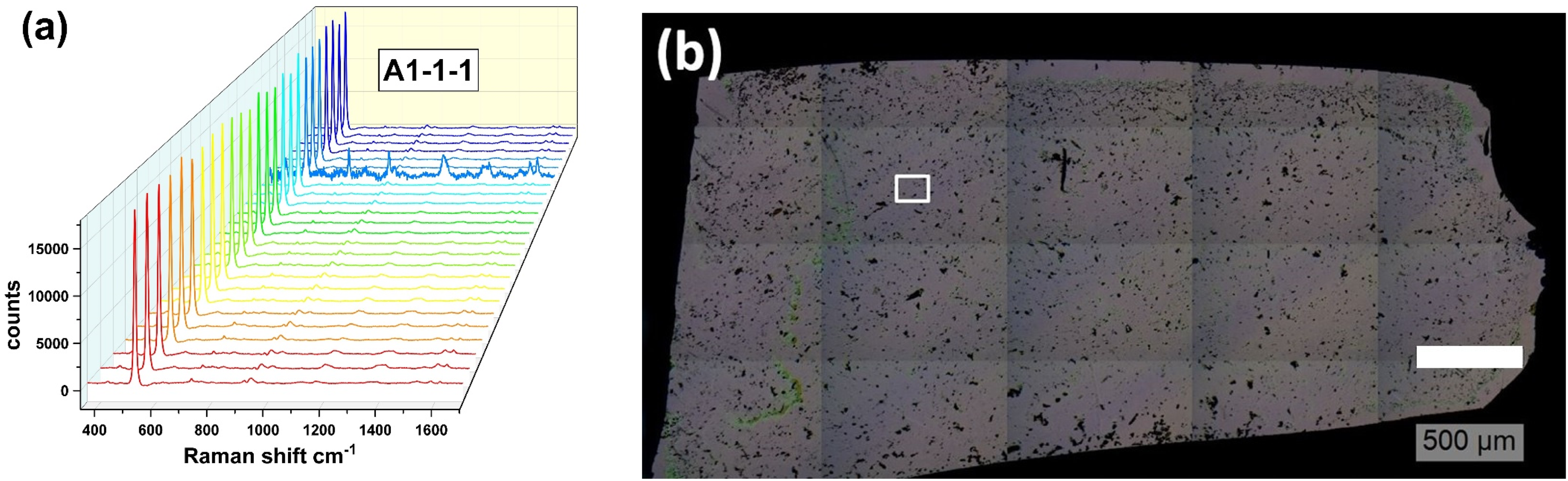
(a) The data set of 25 Raman spectra recorded in one mapping area showing one outlier regarding signal intensity from the probe molecule. (b) Optical image of a typical rectangular specimen showing surface coating by CV molecules. The white rectangle represents one random mapping area, and the black spots are local accumulations of CV molecules.
Because the goal of this study was to conduct an exhaustive investigation of the PhC influence on the Raman signal enhancement, results obtained from every level in the schematic view (Figure 1) were analyzed and compared with each other to check for congruence and reliability of our findings. After the outlier removal, 23–25 spectra were available from each mapping area. Thus, the averaging procedure resulted in nine mean spectra (three mapping areas on three rectangular specimens) for each of the four samples within a particular sample category. These mean spectra were then baseline corrected, using the same positions of zero points for all sample categories, and the results for the typical sample are given in Figure 6. The 10 most prominent Raman CV bands with assignations given in previous works61,62 were used in our study.
The data set consisting of nine mean Raman spectra obtained from sample B1. The ∼520 cm–1 silicon peak is removed for clarity of the y-axis.
Comparable intensities of all Raman bands for different samples within a sample category were found. Figure 7 presents a bar plot of mean Raman band intensities from all four samples and all six sample categories, obtained by Gaussian fitting conducted in Origin. The corresponding table with numerical data is included in Table S1 (Supplemental Material). Every column in a bar plot is a result of averaging nine mean spectra, as shown in Figure 6. For clarity, when comparing the mean intensities of each Raman band on four different samples, the y-axis scales in Figures 7a to 7f are made different. Since the intensities of the ∼520 cm–1 silicon peak are approximately two orders of magnitude higher than the intensities of CV bands, every image has an inset where this peak is removed. Although the overall reproducibility of samples, and hence the data reliability is more than solid, a more detailed look reveals there do exist several peculiarities regarding the mean intensities of several CV bands. For instance, the intensities of all CV bands on sample B3 are the highest, being followed in proper order by mean intensities on samples B2, B1, and B4. On the other hand, and especially for samples within sample categories E and F, the mean intensities of Raman bands do not follow a particular trend where one sample shows their highest and one their lowest intensity. There is also a sample D1 from which significantly lower intensities of several CV bands, compared to the other three samples within the sample category, were recorded. Moreover, the relative ratio of mean intensities of 10 observed CV bands is not the same for different sample categories. These facts further corroborate the statistical approach with many Raman bands using multiple samples conducted in this paper.
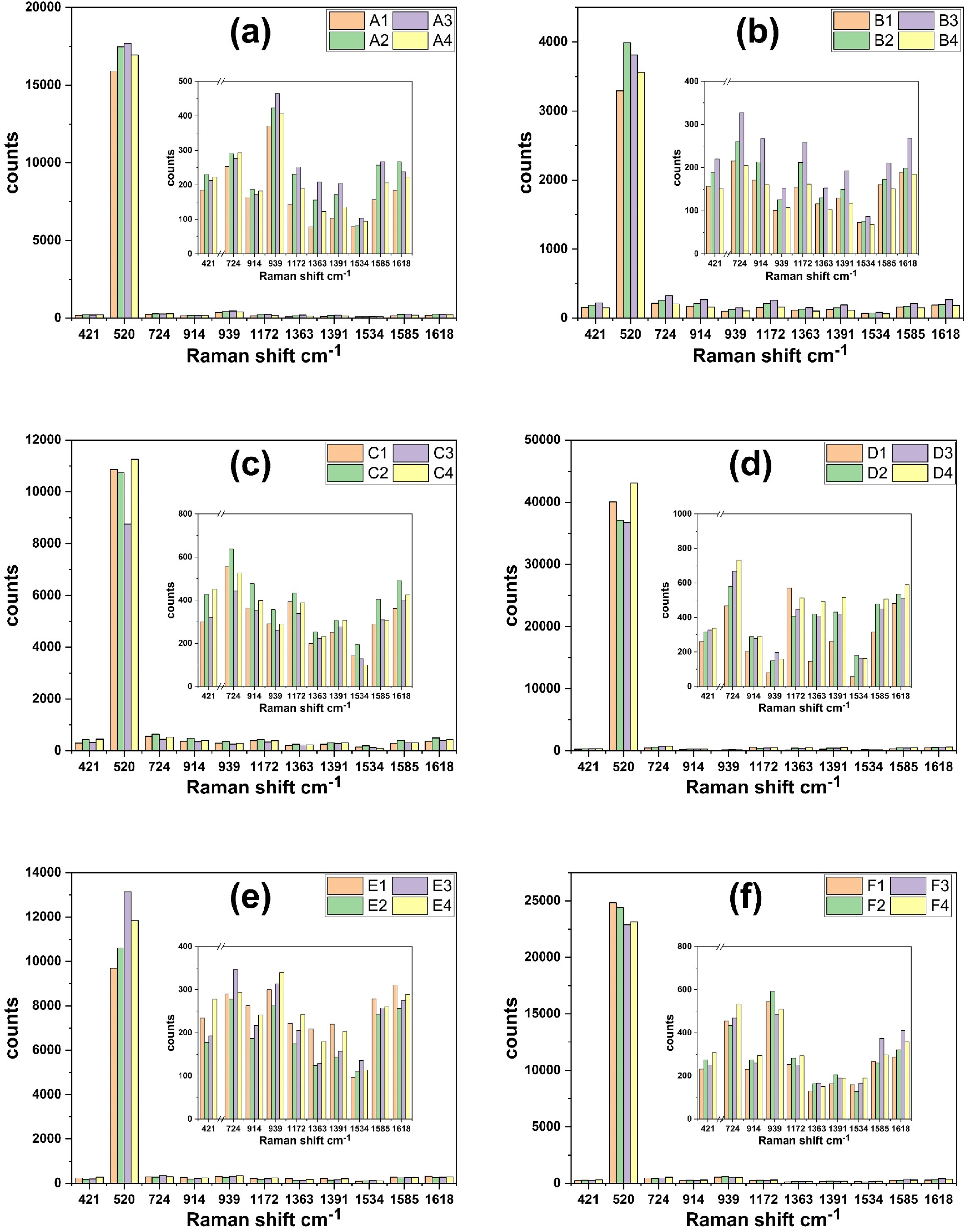
Bar plots representing mean intensities of Raman bands recorded on four different samples (A1–A4, etc.) within six different sample categories (A–F). Images (a)–(f) show data for sample categories A, B, C, D, E, and F.
To get an insight into the consistency of our results, we have also computed and graphically illustrated the exact average values and the corresponding standard deviations for all wavenumbers in each sample category (containing ∼900 spectra), as shown in Figure S2 (Supplemental Material). The discrepancy between the fitted (Figure 7) and the exact values is for most bands in all sample categories <15% except for several bands in sample category D. Moreover, the standard deviation across all Raman bands within one sample category is usually much less than 25% except for bands at 914, 1363, and 1391 cm–1 in sample categories D and F.
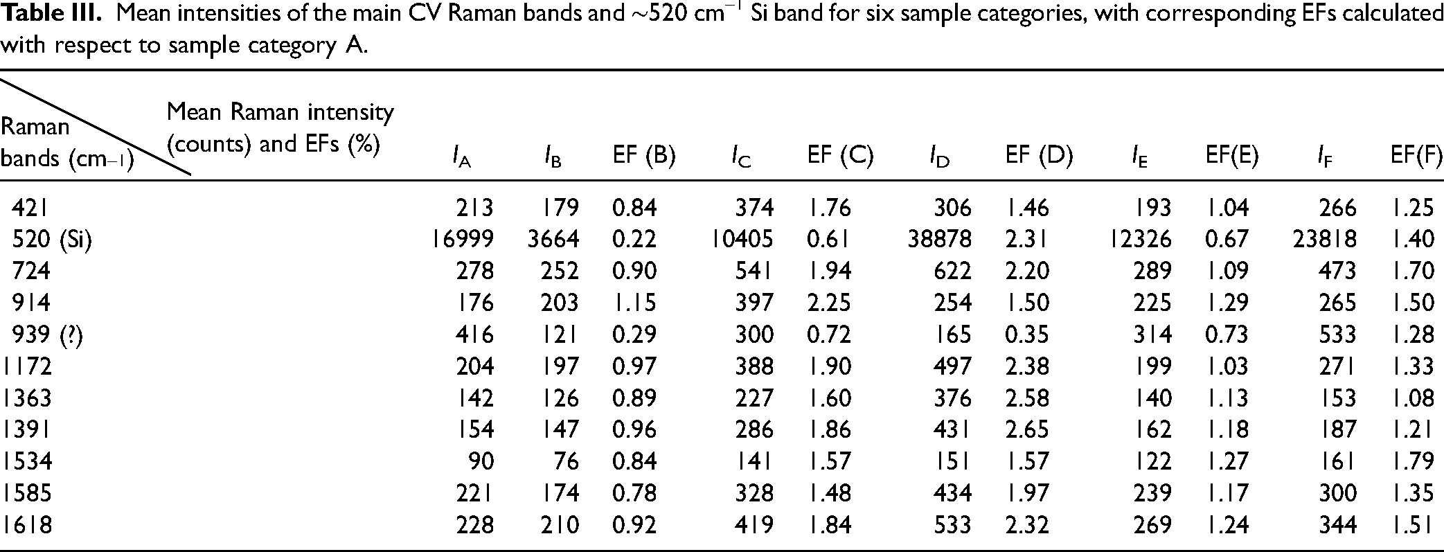
Raman signal enhancement using PhCs was analyzed using the final results summarized in Table III and illustrated in Figure 8. The mean intensity for each Raman band in the spectrum was obtained by averaging ∼900 spectra per sample category, which in total gives ∼5400 spectra for all six categories (error bars represent standard deviation for each band). The EFs were obtained by simple division of the number of counts in a certain cell by the corresponding number of counts for sample category A. Previously published papers reported results that were based on the analysis of just a few spectra and usually only one Raman band (Table I).
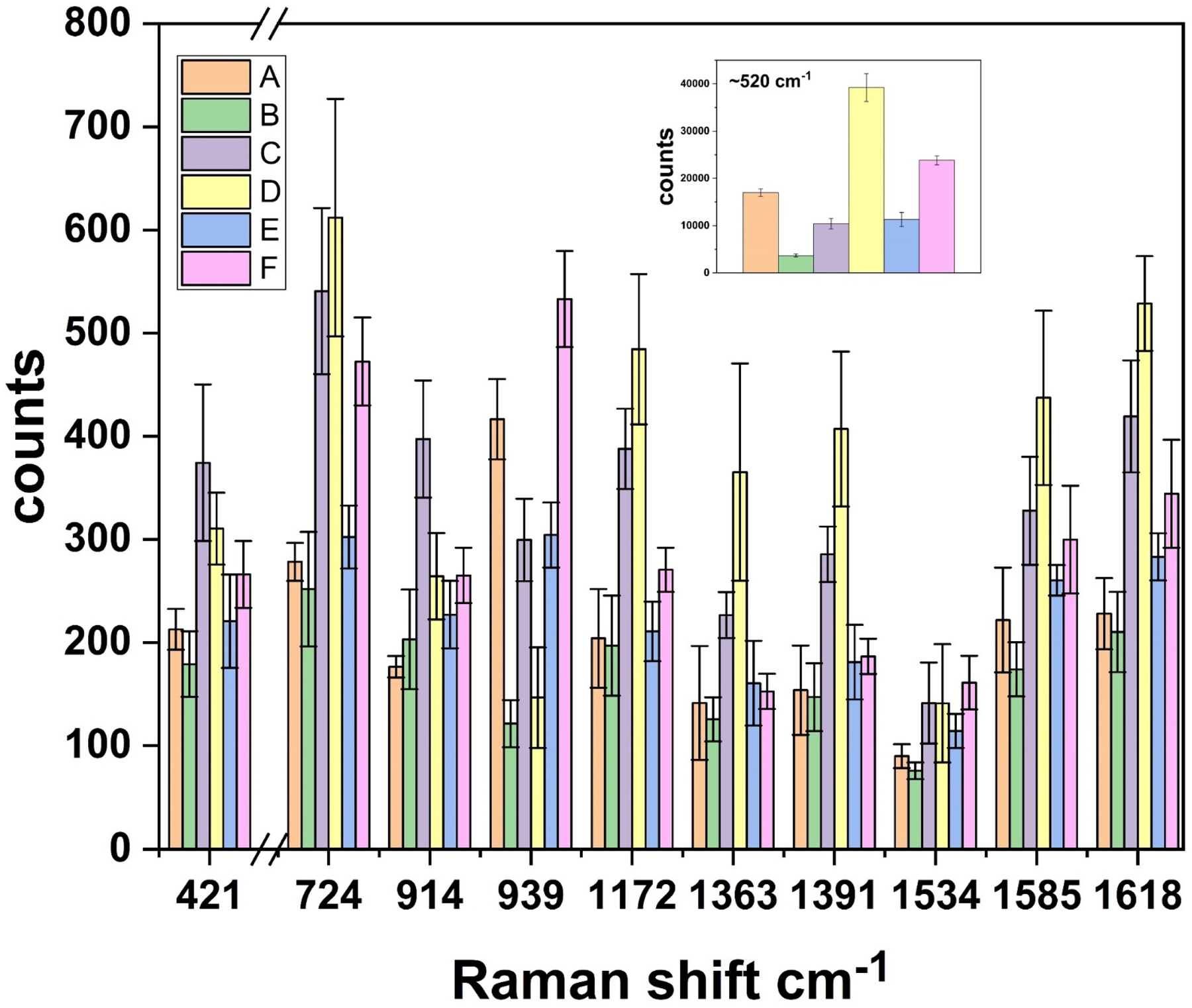
Bar plot illustrating the final mean intensities of the main CV Raman bands for six sample categories and ∼520 cm–1 band highlighted in the inset. Error bars represent the standard deviation for each band.
Mean intensities of the main CV Raman bands and ∼520 cm–1 Si band for six sample categories, with corresponding EFs calculated with respect to sample category A.
The analysis is divided into two parts; one that scrutinizes the intensity of the ∼520 cm–1 silicon Raman peak, corresponding to the material from which the PhCs (and their underlying mechanical support) are made, and one that investigates the Raman signal coming from the probe molecule. Also, in both parts of the analysis, we will primarily discuss the effect of the alignment of laser excitation with specific positions in the PBG, but also will mention the possible stopband's influence on the Raman-shifted bands.
Silicon ∼520 cm–1 Raman Band
The intensity of the silicon ∼520 cm–1 Raman band, related to the scattering by transverse-optical phonons at the center of the Brillouin zone, enables verifying the relative position between the laser excitation and the PBG for sample categories B to F, and was therefore used as a sample category control. The position and shape of this band were the same for all sample categories indicating the phonon confinement effect was negligible. 63 The intensity of the ∼520 cm–1 peak for the ordinary pSi, as sample category A, had only ∼5% variation between samples A1 to A4 (Figure 7a), leading to the overall average of 17 000 counts (Table III). Due to the ∼10 μm penetration depth of the 785 nm laser excitation in pSi samples with a ∼7.5 μm thickness, a part of incident light reaches cSi. Therefore, we can assume that at least one-quarter of the mean number of counts for the ∼520 cm–1 peak in sample category A originated from scattering in cSi.
The laser excitation for sample category B coincides with the center of the reflectance peak, i.e., center of the PBG, and >80% of the incident radiation is reflected (Figure 2b). Hence, only the minor part of the incident radiation is allowed to propagate downward through the PhC and give rise to Raman scattering. As expected, the mean intensity of the ∼520 cm–1 Raman peak is in this case approximately five times lower (3650 versus 17 000 counts) compared to the one from sample category A and fits reasonably well with the reflectance difference between these two sample categories (>80% versus ∼20%). The decrease in the Raman signal of the material from which the PhC is made has also been previously reported. 24 The allowed 5 nm wavelength range, belonging to the predetermined uncertainty interval for each sample category, matched the very top of the reflectance peak and resulted in <10% variability between samples B1 to B4.
Next, it is obvious from Figure 8 that the mean intensity of ∼520 cm–1 peak for sample categories D and F is higher compared to the one belonging to the control category A (∼2.3× for category D and ∼1.4× for category F), while the reflectance is comparable for all three categories. This enhancement of Raman signal of PhCs constituent material, in case of alignment of excitation laser with the edge of the PBG, has been many times predicted by theory, and even several times experimentally observed, but with EFs that covered a wide range of values (Table I). Generally, Compaan and Trodahl 64 showed 40 years ago that the Raman scattered photon rate is directly proportional to the square of Raman susceptibility, an intrinsic property that characterizes the ability of the material to undergo Raman scattering. On the other hand, according to the theory of PhC, there is a much longer light–matter interaction in the case when the laser excitation coincides with the edge of the PBG, explained either as confinement of light or increased EM density of optical states. Consequently, the longer light–matter interaction in the case of sample categories D and F results in a higher probability of Raman scattering, which implies the increase in Raman susceptibility, either of the PhCs building block or of any molecule infiltrated inside PhC. This statement was experimentally confirmed in articles published by a Russian group,26,27,65 which reported an increase in the effective Raman susceptibility and estimated two orders of magnitude longer light–matter interaction time for pSi PhC, ultimately yielding an almost tenfold enhancement for the ∼520 cm–1 silicon peak. Our data confirm that there exists an enhancement of the ∼520 cm–1 peak, but with a modest EF between 1.4 and 2.3, with a higher one corresponding to the alignment of laser excitation with the high-frequency edge of PBG. On the other hand, this difference in EFs between PBG edges is not easily explainable. It can be calculated that the Raman shift of ∼520 cm–1 falls just below the top of the reflectance peak for sample category D, while it falls further away from the PBG edge for sample category F. The corresponding reflectance at these positions are ∼65% and ∼22%, respectively. There have been several reports in the literature stating that the PBG effect inhibits the Raman scattered photons from transmitting through the PhC in the normal incident direction due to the Bragg reflection caused by a periodic multilayer structure.66,67 Therefore, when there is an overlap of certain Raman-shifted bands wavelength shifts with the PBG, the constructive interference of back-reflected Raman scattered light should result in the enhancement of recorded intensity for these bands. Considering this, the intensity of the silicon ∼520 cm–1 band should be higher for sample category D. If this explanation is valid, it also should be kept in mind that the majority of detected Raman-shifted photons came from scattering that occurred in layers closer to the surface since the photons created deeper inside PhC structure would be influenced by the PBG both above and below.
Finally, sample categories C and E correspond to the cases when the laser excitation is aligned with the middle of the reflectance peak on its high- and low-frequency sides, respectively. These two sample categories were used solely due to the inconsistencies in the literature regarding the definition of PBG edge and its possible enhancement of the Raman signal. The bar plots in Figure 8 (and data in Table III) show that the mean intensity of the silicon peak is ∼40% (for category C) and ∼30% (for category E) lower compared to sample category A, again in a good correlation with the reflectance differences between these two sample categories and ordinary pSi. The discrepancy in mean intensities probably came from different plateaus in terms of reflectance on both sides of PBG (Figure 2a) which caused the few percent reflectance variance in the uncertainty wavelength interval corresponding to a particular sample category. Also, aligning the laser excitation with the wavelength interval for these two sample categories was not an easy task. For instance, the variability in the intensity of ∼520 cm–1 peak was the highest for sample category E (Figure 7e), and the C3 sample (Figure 7c) had a strong impact on lowering the mean value of silicon peak for sample category C. Contrarily to the explanation of stopband's influence on the ∼520 cm–1 Raman-shifted photon given in a previous paragraph, the mean intensity for sample category E is higher than the one for sample category C. This result is even more perplexing since the Raman shift of 520 cm–1 falls on the very top of the reflectance peak for sample category C (with reflectance >80%), implying almost all Raman-shifted photons created in superficial parts of pSi PhC should be reflected backward and increasing the total number of counts. On the other hand, the Raman shift of 520 cm–1 falls exactly on the low-frequency edge of the PBG for sample category E. Although it can be expected that these Raman-shifted photons experience a longer light–matter interaction time, it is unclear whether this effect has any influence and why is their mean intensity higher compared to the sample category C.
Ten Most Prominent CV Raman Bands
The analysis of the intensity of the Raman bands coming from the probe molecule CV seems to be more complicated due to the number of observed bands. For instance, as is evident from Figure 8, the signal enhancement is not the same for all Raman bands since some show completely different behavior compared to others, e.g., the band at 939 cm–1. Again, in the analysis, the mean intensities belonging to the sample category A are used as a reference.
By overlapping the center of the PhC reflectance peak with the excitation laser, the logical assumption would be that there exists a double chance for Raman scattering to occur; one coming from the incident and one from the back-reflected light. Due to the high reflectance (∼85%) for sample category B, this double chance corresponds only to the CV molecules adsorbed as a continuous film on the pSi PhC surfaces (Figure 5b) and the anticipated EF for all CV bands was ≤2. Astoundingly and contrary to several published works (Table I), our data show almost identical (in the standard deviation range) mean intensities for nine out of 10 observed CV bands compared to the ordinary pSi. Also, this result casts doubt on the usage of 1D pSi PhCs for the additional photonic part of the enhancement in SERS measurements, because the metal nanostructures for this purpose have been so far deposited exclusively on top of the photonic structure. 68 One possible elucidation for the lack of enhancement lies in the dimensionality; 1D PhCs were utilized in our work, resulting in the creation of the PBG only in the direction perpendicular to the surface. Gaponenko 35 inferred that in the case of 1D PhCs, Raman scattering would be inhibited along the direction where the periodicity exists, but increased in the other two directions, due to the angular redistribution of the photon density of states. Since the objective in our experimental configuration is perpendicular to the surface, analysis of the signal in other directions was inaccessible. Still, the abovementioned statement might be valid for the interior of the PhC and molecules within but does not clarify the case of molecules adsorbed on the surface. Also, it should be noted that the numerical aperture of the objective was rather low (0.25), but it was always the same throughout the experiment.
Similar to the analysis of the ∼520 cm–1 band, the strongest Raman signal enhancement was obtained when the excitation laser overlapped with the PBG edge. Six out of 10 observed CV bands showed the strongest enhancement when the laser excitation coincided with the high-frequency edge of the PBG and two out of 10 for the low-frequency edge. Averaging over the whole spectrum but excluding the unaccountable 939 cm–1 band (mentioned also in the next paragraph) the EF for sample categories D and F would be ∼2.1 and ∼1.4, respectively. The different enhancements obtained when aligning the laser with high- and low-frequency edges of the PBG might also be explained with a theoretical approach. As written in Materials and Methods section, all our pSi PhCs underwent etching with a sinusoidally modulated current density ranging between 1 and 50 mA/cm2. The etching process began at the value of 25 mA/cm2, increased to the maximum and then sinusoidally decreased to the minimum, implying the photonic structure begins with a low-refractive index section and ends with a high-refractive index one. It is possible to conceive the 50 layers (with smooth boundaries of rugate type) that constitute the PhC to be divided into the low-refractive index section closer to the surface and the high-refractive index further from it. Also, the diffusion of CV molecules into the porous structure should produce a concentration gradient in the direction perpendicular to the surface. The inference of this hypothesis is that there should be more CV molecules in the low-refractive index sections of any layer. One of the fundamental theoretical aspects of PhCs3,51 states that high-frequency EM modes undergo localization in low-refractive index layers, while low-frequency modes are localized in high-refractive index ones. As a result, the Raman intensity enhancement is to a certain degree higher for high-frequency edge corresponding to sample category D. In addition, the whole recorded Raman spectrum of CV (<1700 cm–1) falls within the stopband width for sample category D, but since we used a rugate filter with a narrow FWHM, all Raman-shifted bands experience different magnitudes of PBG reflectance.
Finally, aligning the laser excitation with the middle of the reflectance peak on its high- and low-frequency sides yielded higher EF for all CV bands in sample category C. Also, apart from the CV band at 939 cm–1, which showed completely inexplicable intensities (the strongest band in the Raman CV spectrum obtained on the sample category A and diminution of intensity for all PhCs except for sample category F), the EFs for CV bands in sample category C are even higher compared with EFs for sample category F. For instance, there are two low-frequency Raman bands at 421 and 914 cm–1 for which the EF is the strongest of all categories. These two Raman shift bands, with the in-between band at 724 cm–1 again feel the overlap with the top of the reflectance peak which might explain their high mean intensities. However, a closer look at Table III reveals that the EFs for all bands in sample category C do not show a large scatter around a mean EF for this category. This revelation again suggests that the stopband's influence on the Raman-shifted bands is uncertain, if even present, and that the most probable explanation for enhancement regarding sample category C is the localization of high-frequency EM modes in low-refractive index parts of PhC structure layers. On account of this, in the current experiment, it is impossible to confirm with certainty if there does exist the PBG influence on the Raman-shifted bands. Nonetheless, certain conclusions can be made. First, there is a critical role played by the alignment between the laser excitation wavelength and the position in the photonic band gap for observing Raman signal enhancement. Our data indicate that Raman signal enhancement belongs to the molecules that penetrated inside the 1D photonic structure and that there is no Raman signal enhancement for molecules adsorbed on the surface of it. In addition, based on >5000 recorded spectra, it can be claimed that the maximum magnitude of enhancement due to the 1D PhC structure for most observed Raman bands, independent of the theoretical explanation, is up to 150%. Also, due to outliers, Raman signal fluctuations, or particular experimental conditions, a single Raman band or just a few spectra, recorded on a small number of samples, cannot be scientifically accepted as a verification of the PhC influence on the Raman signal enhancement. Furthermore, since the Raman EF for sample categories C and E is for the majority of Raman bands, including and most apparently for ∼520 cm–1 silicon peak, weaker compared to sample categories D and F, we can conclude that the PBG edge and its increased EM density of optical states should be strictly defined as the position at the very bottom of the reflectance peak, and not at its middle. Another assumption on the signal enhancement can be derived from EDX measurements. Figure 4 revealed that the probe molecule penetrated up to ∼3 µm into the PhC structure, so the effect of the longer light–matter interaction comes from ∼40% of the total PhC thickness. Considering this, there is a possibility that if the probe molecule could infiltrate into the whole porous structure, the EF for sample category D would increase compared to ordinary pSi. In general, if the EM field is not confined at the first PhC layers, 69 the higher the penetration depth of both the laser and probe molecules into the PhC, the higher the Raman EF might be, in the case of alignment of laser excitation and PBG edge. Hopefully, this claim could be experimentally confirmed in our next work which includes the usage of pSi PhCs with different thicknesses, lasers with different penetration depths into pSi, and variable infiltration depth of probe molecules.
Conclusion
This study investigates the enhancement of Raman signal from 1D PhCs through the analysis of a vast number of spectra. Experimental results indicate the enhancement of the ∼520 cm–1 Raman band of silicon, representing the constituent material of PhC when the laser excitation aligns with the edge of the photonic band gap, defined as the position at the very bottom of the reflectance peak. When the laser excitation is aligned with the center of the photonic band gap, the ∼520 cm–1 band is less than four times weaker compared to the case of monolayer pSi, explained by the strong reflectance of incident light. The Raman signal from the probe molecule CV, both infiltrated into and deposited on the surface of PhC, is also enhanced for excitation alignment with the PBG edge, and absolutely no enhancement was observed for the alignment with the PBG center. However, the obtained EFs are modest compared to most experimental and theoretical predictions, with a maximum of ≤2.5 for the high-frequency edge. The analysis of the prominent CV Raman band intensities showed that the signal enhancement is not the same for all bands, implying that the previously reported results obtained from only one Raman band are disputable. Although the data tend to negate its existence, the PBG influence on Raman-shifted bands is not conclusively determined in the current experiment. The results of this research suggest the design of both PhC-based Raman and SERS substrates for applications in various fields.
Supplemental Material
sj-docx-1-asp-10.1177_00037028241258101 - Supplemental material for Influence of One-Dimensional Photonic Crystal on Raman Signal Enhancement: A Detailed Experimental Study
Supplemental material, sj-docx-1-asp-10.1177_00037028241258101 for Influence of One-Dimensional Photonic Crystal on Raman Signal Enhancement: A Detailed Experimental Study by Maria Krajačić, Nikola Baran, Ana Tolić, Lara Mikac, Mile Ivanda, Ozren Gamulin and Marko Škrabić in Applied Spectroscopy
Footnotes
CREDiT Author Statement
M.K. and M.Š. were responsible for conceptualization and methodology. M.K. conducted most of the investigation process, visualization, and formal analysis. M.Š., N.B., A.T., and L.M. contributed with sample characterizations, investigation, and visualization. M.Š. supervised the whole process. M.I. and. O.G. administered the project and provided resources for measurement and characterization. M.K. and M.Š. wrote the original draft of the manuscript. All authors reviewed the original draft and approved the final manuscript.
Declaration of Conflicting Interests
The authors declared no potential conflicts of interest with respect to the research, authorship, and/or publication of this article.
Funding
The authors disclosed receipt of the following financial support for the research, authorship, and/or publication of this article: The research was partially supported by the project co-financed by the Croatian Government and the European Union through the European Regional Development Fund Competitiveness and Cohesion Operational Programme (KK.01.1.1.01.0001).
Data Availability
The raw data, and datasets generated and/or analyzed during the current study are available from the corresponding author upon reasonable request.
Supplemental Material
All supplemental material mentioned in the text is available in the online version of the journal.
References
Supplementary Material
Please find the following supplemental material available below.
For Open Access articles published under a Creative Commons License, all supplemental material carries the same license as the article it is associated with.
For non-Open Access articles published, all supplemental material carries a non-exclusive license, and permission requests for re-use of supplemental material or any part of supplemental material shall be sent directly to the copyright owner as specified in the copyright notice associated with the article.