
Abstract
We report the structural and optical characterization of one-dimensional porous silicon microcavities. These structures are based on a planar resonator formed by two high-reflectance mirrors separated by a thin active optical spacer. In order to simulate and predict the optical properties of the microcavity, the transfer matrix method is used. A strong correlation between the formation parameters and the reflectance spectra is introduced. The prepared microcavities are exposed to thermal oxidation. The resonance position of the microcavity exhibits a blueshift proportional to the degree of oxidation. Structural changes of the microcavities after oxidation are investigated and analyzed using X-ray diffraction and Raman spectroscopy. The observed shift of characteristic silicon peak is attributed to the reduction of silicon crystallites as the oxidation increases.
Introduction
Porous silicon consists of a mixture of silicon nanostructures and voids. It controlled electrochemical etching of single crystalline silicon wafers in hydrofluoric (HF) acid electrolyte. 1 This material has gained much interest after the discovery of its emission room temperature luminescence. 2 The observed luminescence from porous silicon opened the door for a variety of applications. Koshida and Koyama introduced the first light emitting diode (LED) device made of metal/porous silicon junction with only 10−5% external quantum efficiency. 3 Quite high electroluminescence efficiency was readily obtained with liquid electrical contacts as first reported by Halimaoui et al. 4 Unfortunately, liquid contacts are of no practical interest in optoelectronic applications. In addition, the luminescence degradation using liquid contacts is much faster than with solid contacts. In 1995, the second generation of LED was more successful and was based on a heterojunction formed between porous silicon and silicon. 5 The third generation of devices with high efficiencies and long duration was based on post-etching oxidation. 6 Integration of porous silicon-based LED with conventional microelectronics circuitry has been demonstrated. 7 Highly sensitive photodetectors and optical logic gates have been fabricated from porous silicon. 8,9 In addition to its optoelectronics applications, there are many possibilities for many potential applications of porous silicon such as waveguides, 10 capacitors, 11 and bioactive implants. 12
Porous silicon microcavity, on the other hand, offers the opportunity to sharpen the broad luminescence of porous silicon. 13 The creation of optical microcavity from porous silicon can be performed by varying the anodization conditions in a direction perpendicular to the surface. The structure of the microcavity, also named Fabry–Perot filter, consists of two parallel mirrors separated by a spacer layer, whose optical thickness can be either λ or λ/2. 14 In this way, a planar microcavity is obtained with a single-photon mode. 15 The reflectivity spectrum of the microcavity is characterized by a narrow transmission line centered between two highly reflecting bands. Microcavities can be exploited as band-pass filters with a tunable narrow transmission line. 16,17 In addition, they can be utilized as highly sensitive detectors for chemical vapors and biosensors. 18 –22
It has been observed that the storage of porous silicon films in ambient air causes uncontrolled oxidation. The silicon partially turns into silicon dioxide (SiO2), and consequently the properties of porous silicon are changed. 23 In this work, we report the precise formation of porous silicon microcavities and investigate their structural and optical properties. Controlled thermal oxidation is performed on the prepared microcavities. The evolution of the spectral features as a function of oxidation is investigated. The obtained spectral response is simulated using the transfer matrix method. The structure changes upon oxidation are explored using X-ray diffraction (XRD) and Raman spectroscopy.
Experimental section
Porous silicon microcavities have been formed by electrochemical etching of p+-type silicon wafers (resistivity is 0.01–0.02 Ω·cm) in 20 wt% HF in ethanol. Before anodization, the silicon samples were dipped in propanol and cleaned in an ultrasonic bath. The samples were immersed in distilled water and dipped in 5 wt% HF acid for 7 min to remove the native oxide. Each silicon substrate was fixed horizontally in a Teflon-made anodization cell with an O-ring at the bottom that allows an effective electrode area of 0.95 cm2. The counter electrode was in the form of a platinum rod. After anodization, the sample was rinsed with pure ethanol and dried using nitrogen gas. A computer-controlled current source (Keithley 6221) was used to supply the necessary current. The morphology and thickness of the prepared samples were investigated using a scanning electron microscope (SEM; Quanta FEG 250, Hillsboro, OR, USA). All reflectivity data are taken in the wavelength range of 190–2500 nm, using JASCO V-570 spectrophotometer (JASCO, Int. Co., Ltd., Tokyo, Japan).
Thermal oxidation of the prepared samples is performed in a tube furnace for 5 min in ambient atmosphere at different temperatures. XRD was investigated using a high-resolution Empyrean powder diffractometer (PANalytical, Almelo, Netherlands). The source of X-ray was CuKα 1 (λ = 1.540Å) and CuKα 2 (λ = 1.544Å) radiation. Raman measurements were performed using Senterra Raman microscope (R200-L, Bruker Optics, Ettlingen, Germany). The incident wavelength and laser power were 532 nm and 10 mW, respectively. The instrument resolution is 9.8 cm−1.
Results and discussion
Porous silicon microcavity was prepared by forming two rugate mirrors separated by central layer. Each rugate mirror was etched using a sinusoidal current density signal oscillating between 5 mA cm−2 and 110 mA cm−2 with a frequency of 0.2 Hz. In order to estimate the refractive index of the microcavity layers, several individual porous silicon layers were formed at different current densities. The porosity P of the individual layers was obtained gravimetrically. 24 The refractive index of each layer is determined from Bruggeman formula given by 25

where n air, n si, and n layer are the refractive index of air, silicon, and the effective medium of the layer, respectively. The top mirror of the microcavity was prepared using nine cycles, whereas the bottom mirror is formed using eight cycles. Figure 1(a) shows the cross-sectional SEM image of the prepared microcavity. The central layer was prepared by applying a constant current density of 55 mA cm−2 for 6 s corresponding to a refractive index of 2.14. The corresponding reflectance spectrum of the prepared microcavity is displayed in Figure 2(a). The spectrum shows a sharp resonant transmission band at 852 nm. The resonance position λ is quite consistent with the relationship


(a) The cross-sectional SEM images of porous silicon microcavity having a slight difference in thickness of the top and bottom mirror. The top and bottom mirrors were prepared using nine and eight sinusoidal cycles, respectively. (b) Cross-sectional SEM images of the microcavity prepared using the same conditions as (a) but with the top and bottom mirrors having identical thickness corresponding to 12 sinusoidal cycles. SEM: scanning electron microscope.

(a) The measured and simulated reflectance spectra of the porous silicon microcavities whose mirrors having slight different thickness (9 and 8 cycles) and (b) that composed of two mirrors having identical thickness (12 cycles).
where m, n c, and d c are the order of the spectrum, the refractive index, and the thickness of the central layer, respectively. The resonant wavelength is sandwiched between two reflectance bands having different intensities as shown in Figure 2(a). The higher intensity band corresponds to the thicker rugate mirror. The reflectance intensity is enhanced as the number of rugate layers increases. 26 This result indicates that any slight difference between the thickness of the top and bottom mirrors affects significantly the characteristic reflectance spectrum of the microcavity. Figure 1(b) shows the SEM image of a microcavity composed of two rugate mirrors prepared using the same conditions and having identical thickness (12 sinusoidal cycles). The corresponding reflectance spectrum displays a sharp dip between two identical reflectance maxima as shown in Figure 2(b). The reflectance maxima reach the same intensity due to the identical thickness of rugate mirrors. The simulated reflectance spectrum was performed using a transfer matrix method. 27 In this method, each layer constituting the microcavity is represented by a matrix that can be expressed in terms of the thickness and refractive index of the layer. The calculated reflectance is obtained by multiplying the matrices of all layers. The simulated reflectance spectrum is in good agreement with the experiment one in terms of the resonance position and the intensity of the reflectance maxima as shown in Figure 2. However, the measured spectra show less intense sidebands at wavelengths lying outside the microcavity band. This can be attributed to the effect of absorption which was neglected in the simulation process. The extinction coefficient of porous silicon reaches its smallest value of 0.05 in the wavelength range from 700 nm to 900 nm. 28 Outside this range, the extinction coefficient becomes higher and highly sensitive to the wavelength. Such an effect was not included in the simulation. We performed the simulation by neglecting the extinction coefficient and utilizing only the real parts of the refractive index. This assumption could be resonance within the operating wavelengths of the microcavity and is not valid at other wavelengths.
For the sake of maintaining the optical features of the microcavity, the structure has to be protected against uncontrolled ambient oxidation. For this reason, the prepared structure was exposed to controlled thermal oxidation. Figure 3(a) shows the reflectance spectra of prepared porous silicon microcavity and that recorded after thermal oxidation at 350°C, 550°C, 750°C, and 950°C for 5 min. The resonant band of the thermally oxidized microcavity at 350°C exhibits a blueshift by 2.17%. The amount of blueshift increases as the oxidation temperature rises. The characteristic spectral features of the microcavity oxidized at 950°C disappear and show instead of distinct interference fringes as depicted in Figure 3. After oxidation, the structure of porous silicon microcavity is composed of a mixture of silicon, air, and SiO2 (n SiO2 whose refractive index is 1.45). For this reason, Bruggeman formula (equation (1)) can be rewritten

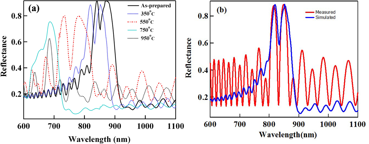
(a) The reflectivity spectrum of as-prepared porous silicon microcavity and that oxidized at different temperatures for 5 min. (b) Measured and simulated reflectivity spectra of a porous silicon microcavity oxidized at 350°C for 5 min.
where F air, F SiO2 , and F Si are the volume fractions of air, SiO2, and silicon remaining after oxidation, respectively. When some part of silicon x has been converted to SiO2, the remaining volume fraction of silicon, F Si, is 1−p−x. Since the silicon and SiO2 have nearly the same density of 2.3–2.2 gcm−3, respectively, the combination of two moles of oxygen for every mole of silicon creates a 2.27-fold increase in the volume of the solid matrix. This increase of volume yields a volume fraction of SiO2 with 2.27x. Thus, equation (3) can be expressed as

At a very high degree of oxidation, the volume increase of the solid matrix becomes higher and leads to the collapse of the porous structure. This is consistent with the disappearance of the spectral features of the microcavity oxidized at 950°C for 5 min as shown in Figure 3. The change in the refractive index of each layer constituting the microcavity upon oxidation can be estimated using equation (4). We assume that oxidation proceeds uniformly through the thickness of the microcavity and use the transfer matrix method to calculate the reflectivity spectrum at different volumetric fraction, x, of the oxidized silicon. Figure 4 shows the evolution of the resonant pass band centered at 852 nm as a function of the fraction of oxidized silicon. The blueshift observed by this band upon oxidation at 350°C can be linked to the transformation of 2.5% of silicon into SiO2 as indicated by the good agreement between the simulated and measured reflectivity spectra (Figure 3(b)). Increasing of the fraction of SiO2 leads to more blueshift of the resonant band. The amount of the blueshift is proportional to the oxidation temperature which determines the amount of silicon that is transferred to SiO2. As the oxidation temperature is increased, a fraction of the silicon pore walls is converted to SiO2, which causes the refractive index to decrease and the resonance wavelength to shift to shorter wavelengths. This resonance shift is a passive wavelength shift in the sense that it is a permanent, irreversible effect. The more the sample is oxidized, the larger is the blueshift. 29,30 The oxidation process can be used to tune the wavelength of the microcavity, which is useful for application that requires the resonance to be at a specific wavelength. It is hard to account for the thickness increase of each layer of the microcavity in the above calculations as the function of the oxidation treatment. For this reason, Figure 4 does not predict the collapse of the porous structure at high degree of oxidation as indicated by the sample oxidized at 950°C (Figure 3(a)). Figure 5 displays the top-view SEM images of the porous silicon microcavity oxidized at different temperatures. A moderate oxidation temperature of 350°C is accompanied by a reduction of the pore size as shown in Figure 5(b). Severe oxidation temperature at 950°C brings different morphologies to the surface. The majority of pores are merged together. This observation is consistent with the disappearance of the spectral features of the microcavity as shown in Figure 3(a).

Simulated variation of the resonant wavelength of a porous silicon microcavity as a function of the volume fractions of oxidized silicon.
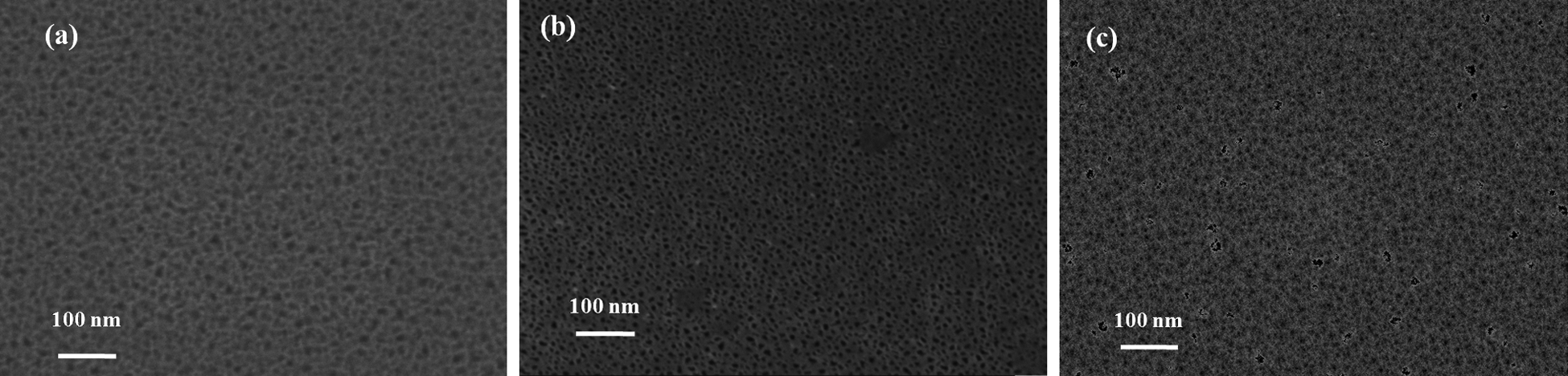
(a) Top-view SEM image of an as-prepared microcavity and that oxidized at 350°C (b) and (c) at 950°C for 5 min. SEM: scanning electron microscope.
In order to explore the crystal structures of oxidized porous silicon microcavity, θ−2θ XRD analyses were carried out. Figure 6 shows the XRD pattern for as-prepared porous silicon and that of the thermally oxidized sample at 350°C and 950°C for 5 min. The obtained diffraction patterns are compared to that pattern of the starting silicon substrate. The substrate displays two distinct diffraction peaks at 69.26° and 69.40°. These two peaks originate using CuKα
1 (λ = 1.540Å) and CuKα
2 (λ = 1.544Å), respectively. When some corrections for CuKα
2 are performed, only a single peak can be left as reported by Aouida et al.
31
As-prepared microcavity exhibits an additional small peak at lower angle which can be ascribed to the porous silicon formation.
32
Some porous silicon samples prepared by Sudesh et al. showed only a single peak at the position of the bulk substrate.
33
Their result implies that there is no lattice mismatch between the film and the substrate where the average lattice parameter of the porous layer is the same as that of the bulk silicon substrate. This means that neither a lattice expansion nor contraction occurs. However, our obtained low-angle diffraction peak can be attributed to a lattice expansion. The change in the 2θ angle of 0.068 represents a lattice expansion (Δa/a) of 4.5 × 10⁻⁴, which is consistent with the magnitude of the previous reports.
34
As shown in Figure 6, the greater the oxidation, the more the porous silicon microcavity peak deviates from the silicon substrate peak. This indicates the increase of the lattice mismatch upon the growth of SiO2. The lattice expansion (Δa/a) is linked to the fraction of the SiO2


XRD pattern of (a) p+-type silicon substrate, (b) porous silicon microcavity, (c) thermally oxidized microcavities at 350°C, and (d) at 950°C for 5 min. XRD: X-ray diffraction.
where α is a parameter depends on the ratio between the Si–Si distance in the oxidized porous silicon and that in unoxidized silicon. Equation 5 implies that the lattice mismatch has a direct impact on the resonance characteristics of the microcavity. The observed blueshift of the resonance line is attributed to the increase of the volume fraction of the SiO2 (equation (3)). The volume increase is accompanied by the increase of lattice mismatch. The porous silicon peak gets broader as the oxidation temperature increases. This gives an evidence of the reduction of the silicon crystallite in porous silicon upon oxidation as can be quantitatively explained by Debye–Scherrer’s relationship. 36
Figure 7 shows the evolution of the Raman spectra with the oxidation temperature of porous silicon microcavity. The Raman peak is obviously red-shifted and broadened asymmetrically with increasing the oxidation temperature. As the temperature increases, the silicon particles are further oxidized, which means that the silicon grain size gradually decreased as the SiO2 layer gets thicker. The reduction of silicon crystallites upon oxidation has been implied by the XRD results. Upon the reduction of the grain size, phonon can be confined in space by crystal boundaries or defects. The conservation of phonon momentum is violated, allowing a contribution from phonons with a non-zero wavenumber to the Raman spectrum. This results in red-shifted Raman peak with asymmetric broadnenig. 37,38 Such a behavior has been reported for the Raman spectra of silicon nanowires as the diameter of the nanowires gets smaller. 39

Raman Spectra for p+-type silicon substrate, as-prepared porous silicon microcavity, and thermally oxidized microcavity at 350°C and 950°C for 5 min.
Conclusions
In this article, we successfully prepared porous silicon microcavity by appropriate selection of suitable anodization conditions. The spectral features of the microcavity are sensitive to the thickness of the top and bottom mirror of the microcavity. A slight difference between the thickness of the top and bottom mirror of the microcavity has a significant impact on the spectral features of the microcavity. Thermal oxidation of the porous silicon microcavity is accompanied by the reduction of the porosity and the increase of lattice mismatch between the microcavity and its substrate. The resonance position of the microcavity exhibits a blueshift as the degree of moderate thermal oxidation increases due to the formation of SiO2 which render the effective refractive index of the microcavity smaller. This fact can be exploited in tuning the resonance position of the microcavity. Stronger thermal oxidation of the microcavity is not preferred because it is associated with the collapse of the porous structure and disappearance of the spectral features of the microcavity.
Footnotes
Declaration of conflicting interests
The author(s) declared no potential conflicts of interest with respect to the research, authorship, and/or publication of this article.
Funding
The author(s) received no financial support for the research, authorship, and/or publication of this article.