
Abstract
A CMOS body-bias generating circuit has been designed for generating adaptive body-biases for MOSFETs in CMOS circuits for low voltage operation. The circuit compares the frequency of an internal ring oscillator with an external reference clock. When the reference clock is “high,” forward body-bias is generated. When the reference clock is “low,” a reverse body-bias is generated. The forward body bias is limited to no more than 0.4 V to avoid CMOS latchup. The reverse body bias is limited to 0.4 V and is very effective in suppressing the subthreshold current. The frequency adaptive body-bias generator circuit has been implemented in standard 1.5 μm n-well CMOS technology and simulated using SPICE. Excellent agreement is obtained between the simulated output characteristics and the corresponding experimentally measured behavior. It is also demonstrated that up to 90% leakage current in CMOS circuits can be reduced by applying the adaptive bias generator to lower threshold voltage CMOS circuits. The design is simple and can be embedded in low power CMOS designs such as the physical nodes of wireless sensor networks.
Introduction
Recently the substrate (body) of a MOSFET has been the subject of intensive research since body-biasing conditions benefit the CMOS chip design for low power applications [1–3]. The method can be applied in the designing of energy efficient physical nodes in wireless sensor networks [4]. Varying body-bias is a key method to vary the threshold voltage of a MOSFET. From the physics of MOS devices, forward body-bias is known to lower the threshold voltage of a MOSFET. The supply voltage can be reduced or the operational frequency can be increased without scarifying the system performance. However, the forward body-bias increases the leakage current which contributes significantly to power dissipation in high density chips. With the current trend of scaled down CMOS technology, therefore, reduction of the leakage current in a MOSFET has become an important issue. A few approaches have been reported to reduce the leakage current in a MOSFET [3, 5] including the multi-threshold voltage process [5, 6]. Low threshold MOSFETs are used in critical paths of a CMOS circuit design and in non-critical paths, high threshold MOSFETs are used. Assaderaghi et al. [3] have proposed a dynamic threshold MOSFET in which the body terminal is tied to the gate so that MOSFETs are forward body-biased when the transistor is “on” and reverse biased when the transistor is “off”. In the reverse body-bias condition, the threshold voltage is increased, thus leakage current is reduced.
However, the multi-threshold voltage process is not a cost-effective process. On the other hand, dynamic threshold MOSFETs are limited to ultra-low voltage operation since forward body-bias above 0.4 V may turn on the P-N junction between the source and the substrate and may cause CMOS latchup [1]. In this work, a simple adaptive body-bias technique is proposed. When high performance is not needed, the reduction of leakage current is achieved by switching the body-bias from a forward-bias to a reverse-bias condition, adaptively.
Body-bias Technique
A forward body-biased MOSFET [7] can be operated at a lower voltage or higher operational frequency, which is described from the following threshold voltage equation of an n-channel MOSFET,

where VT, N0 is zero bias threshold voltage, γ is body effect factor, VSB is source to substrate voltage, and ΦF = - (EF-Ei)/q is Fermi potential. Here, q is the magnitude of an electron charge and EF and Ei are respectively the values of Fermi energy in the substrate and in intrinsic material. In an n-channel device, 2ΦF ≍ 0.7 V and γ ≍ 1 V1/2. Normally, VSB 0, resulting in VT, N VT, N0. With forward substrate bias (VSB 0), VT, N is less than VT, N0. Thus, a MOSFET can be designed to operate at a reduced voltage or higher frequency. There is a limit to the amount of VSB, which can be applied due to CMOS latchup. In an earlier work, it has been reported that if the source to substrate junction forward voltage is less than 0.4 V, it will not cause latchup of CMOS circuits [1]. Figure 1(a) shows the latchup current versus forward bias voltage. The latchup current is relatively low when forward biased source-substrate is below 0.4 V. Figure 1(b) shows the reduction in threshold voltage with increasing forward body bias in a p-MOSFET.
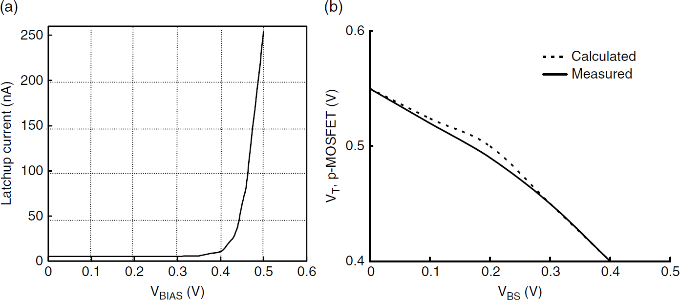
a) Latchup current versus forward body-bias in an n-MOSFET, b) Threshold voltage variation versus forward body-bias in a p-MOSFET.
By reducing the threshold voltage, the leakage current increases and static power dissipation increases which needs to be reduced. The leakage current can be controlled adaptively by switching to a reverse body-bias condition when a system is not required to run for its maximum performance. The adaptive body-bias generator circuit is described in the following section.
Figure 2 shows the block diagram of an adaptive body-bias generator. A reference clock signal is needed to represent the system frequency. When the frequency of the reference clock is set “high,” a forward body-bias is preferred. When the frequency of the reference clock is set “low,” a reverse body-bias is preferred. Adaptive body-bias generator is designed in such a way that it can generate body-biases depending on operating conditions.

Block diagram of an adaptive body-bias generator. Note: VDD = 3.0 V and VSS = 0.0 V.
In Fig. 2, the ring oscillator generates a clock signal. The 3-bit counter counts when the reference clock goes low (“0”). When the reference clock goes high (“1”), data of the counters are stored in a 3-bit positive-edge triggered D-flip flop and then the counter is reset to zero. The ring oscillator can be designed in such a way so that the counter initially counts 3 pulses with the reference clock, fo and Vbias,3 is selected through a 8-to-1 multiplexer where Vbias,3 is a zero-biased body voltage. There are 8 levels of body-biases, Vbias,0 to Vbias,7 and can be selected depending on the output of the D-flip flop. The 8-level binary body-biases, Vbias,0 to Vbias,7 vary from a forward body-bias of +0.3 V to a reverse body-bias of −0.4 V with a decrement of 0.1 V.
Initially zero body-bias, Vbias,3 is selected. With the increasing operational frequency which is given by the reference clock, the counter counts less number of pulses and Vbias,2 to Vbias,0 may be selected. With decreasing operational frequency of the reference clock, the counter counts more number of pulses and Vbias,4 to Vbias,7 may be selected to provide a reverse body-bias for lowering the leakage current. Table 1 shows the truth table of an 8-to-1 multiplexer which generates body-bias for p-MOSFETs.
Truth Table of a 8-to-1 Multiplexer
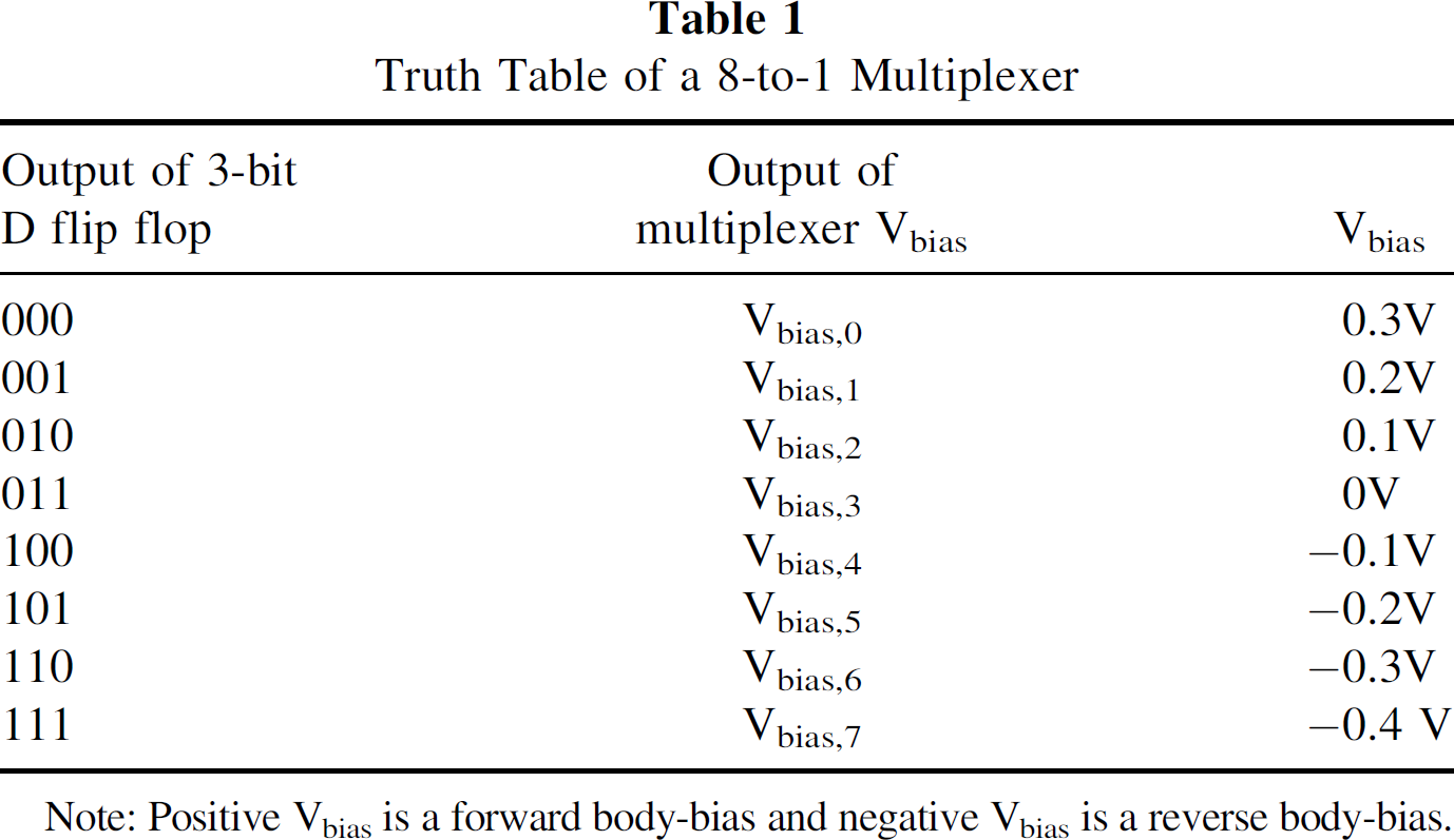
Note: Positive Vbias is a forward body-bias and negative Vbias is a reverse body-bias.
Figure 3 shows an operational timing diagram of the adaptive body-bias generator circuit of Fig. 2. The clear signal has a time delay to ensure D-flip flop samples counter's outputs before counter is cleared. The 3-bit counter is designed to count 000 to 111 and will keep 111 before being reset to zero. A regular 3-bit counter shown in Fig. 2 has been modified as shown in Fig. 4 to perform the counting function in Fig. 3. The counter in Fig. 4 counts from 000 to 111. Before the output reaches 111, the select signal remains high (“1”). Vout from the ring oscillator is selected to trigger the counter. When 3-bit output Vout, is 111, the select signal is low (“0”). No clock triggers the counter since the clock output from 2-to-1 MUX is “0” and 3-bit Vout remains at 111.
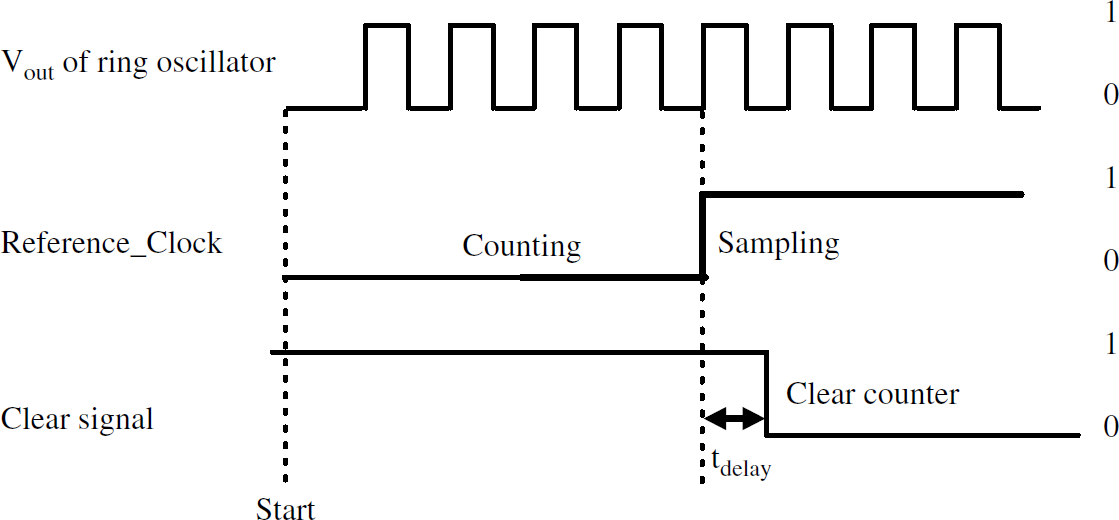
Operational timing diagram of the adaptive body-bias generator.

Logic diagram of a 3-bit counter design.
Figure 5 shows the measured adaptive body-bias versus reference clock frequency of a p-MOSFET. The 8-level body-bias varies from −0.3 V to +0.4 V with 0.1 V increment. In the design, initially the counter counts 3 with fo of 270 kHz.

Body-bias of a p-MOSFET versus reference clock when initially counter counts 3. Note: Vbias,3 = 0V.
A number of simple inverters with varying threshold voltages are used to simulate the leakage current. The body-bias output from the circuit of Fig. 2 has been applied to a p-MOSFET in Fig. 6 for illustration in the leakage current reduction. In the present work, the body-bias could be applied to a p-MOSFET only because the single n-well process does not allow forward-body bias to be applied to n-MOSFETs.
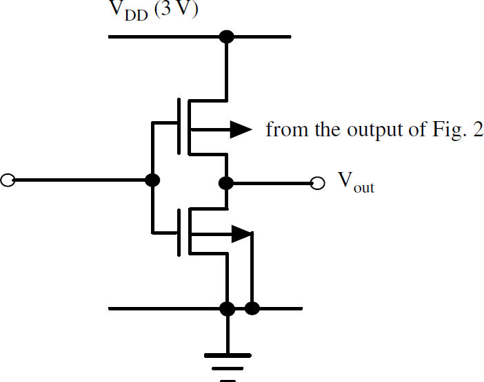
A simple inverter to illustrate leakage current reduction. W/L of a unit size n-MOSFET = 2.4/1.6 and p-MOSFET = 4.8/1.6.
Figure 7 shows the leakage current reduction by providing a reverse body-bias of 0.4 V to the p-MOSFET of the inverter with n-MOSFET W/L ratio of 2.4/1.6 and p-MOSFET W/L ratio of 4.8/1.6. The solid line shows the leakage current with a zero body-bias and the dotted line shows the leakage current with a reverse body-bias of 0.4 V. The leakage current increases with decrease in threshold voltage and the increase is significant for lower threshold voltages. Notable is the increase in leakage current below 0.4 V without body-bias. However, the reverse body-bias is very effective in reducing the leakage current in lower threshold voltages below 0.4 V. It is shown that the adaptive body-bias method is very effective in leakage current reduction in low threshold voltage CMOS circuits.

SPICE simulated leakage current versus initial zero-biased threshold voltage. Note: Solid line represents the leakage current without the reverse body-bias. The dotted line represents the leakage current with the reverse-body bias. VT0 is a zero-bias threshold voltage.
Figure 8 shows the layout of an adaptive body-bias generator CMOS circuit. The layout area is 1.5 mm × 1.5 mm in standard 1.5 μm CMOS process. The microphotograph of the fabricated chip is shown in Fig. 9. Figure 10 shows the output waveform of the 3-bit counter and reference clock. In Fig. 10, the least significant bit (LSB) of counter is observed. The counter starts counting when the reference clock is low, (“0”) and stops counting when reference clock goes high, (“1”). In Fig. 10, the counter counts 4. Table 2 shows the truth table of LSB of the 3-bit counter. The 3-bit outputs of counter are then transferred to D-flip flops to select a proper body-bias through the multiplexer.
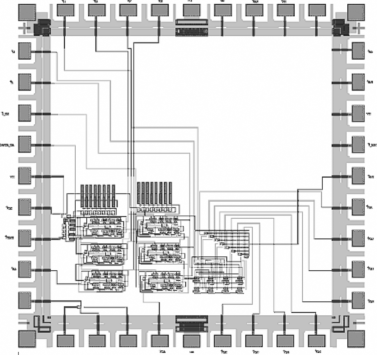
Layout of an adaptive body-bias generator CMOS circuit.

Microphotograph of an adaptive body-bias generator CMOS circuit of Fig. 8.

Measured waveforms of the least significant bit of the counter and the reference clock. Scale: X-axis: 1μs/div., Y-axis: 1 V/div.
Truth Table of a 3-bit Counter

A frequency adaptive body-bias generator CMOS circuit has been designed, which generates varying body-biases to MOSFETs depending upon the operational frequency. The design is based on frequency comparison of an external reference clock and a pre-designed ring oscillator. Notable reduction in leakage current can be obtained for low threshold MOSFETs. The leakage current is reduced 90% in low threshold MOSFET circuits. The adaptive body-bias generator circuit occupies an area of 1.5 mm × 1.5 mm in standard 1.5 μm n-well CMOS process. The design is verified experimentally. The method can lower the leakage current in the CMOS chip when the circuit is not operating at its maximum performance. The presented method is simple and can be embedded in a CMOS system design for low voltage operation such as the physical nodes in wireless sensor networks. In the present design, range of Vbias,0 to Vbias,7 is external to the 8-to-1 multiplexer part of the circuit of the adaptive body-bias generator.