
Abstract
Electroless nickel (Ni) immersion gold (Au), commonly referred to by the acronym ENIG, is the most common protective coating applied on the exposed copper (Cu) traces of printed circuit boards (PCBs). In this work, we elucidate the local corrosion mechanism of the ENIG-Cu system by applying microscopic, surface analysis and electrochemical techniques with high spatial resolution to provide a comprehensive understanding of the complex local corrosion mechanism of the ENIG-Cu system. The corrosion initiation is highly localised and associated with pores or micro-defects in the Au layer. The corrosion initiates by the dissolution of the underlying Ni layer, being less noble than Au. The dissolution propagates in lateral and perpendicular directions relative to the surface in an elliptical fashion. With time, the direction of corrosion propagation changes to a predominantly lateral attack of the Ni layer. The corrosion process is governed by the cathode/anode ratio of the Au/Ni galvanic couple.
Introduction
In an era of highly sophisticated electronic and communication technology, electronic devices have extended to all aspects of our daily life. As a non-volatile data storage device, Secure Digital (SD) memory cards upgrade the storage capacity of electronic devices such as smartphones, digital cameras, tablets, etc. The central part of every SD memory card consists of a printed circuit board (PCB) that includes metallic pins [1,2]. Considering the electronic application of every single PCB in an integrated system, a specific number of circuits are mounted on a plastic backbone. Electronic PCB components such as resistors, capacitors and inductors are connected through Cu traces that conduct electrical currents. However, as they are used in many potentially corrosive service environments, the oxidation of non-embedded Cu without protective coating is highly probable [3 5]. Moreover, the functional integrity of electronics is not only affected by the corrosion of Cu in itself, but also by electrochemical migration and redeposition of dissolved Cu ions on a neighbouring Cu electrode, due to oxidation of Cu and the presence of an electric field potentially jeopardising the reliability of electronics in service [6–9].
Preserving the electronic performance of SD memory cards from corrosion attacks is of great importance. The corrosion rate of metallic pins in the SD memory cards is determined by their final finishing and service environment characteristics. Electroless nickel immersion gold (ENIG) is the leading surface finish used in electronic industries, among other types of final finishing such as hot air solder levelling, organic solderability preservatives, immersion tin, immersion silver, etc. ENIG consists of a bi-layered metallic coating of Ni and Au to protect the Cu traces [10,11]. ENIG is characterised by high resistance to corrosion and whisker growth, excellent electrical conductivity and solderability, and represents a lead-free, environmentally friendly fabrication process [1,12 14].
The intermediate Ni layer between the Cu and Au acts as a barrier against the interdiffusion of Au and Cu. Interdiffusion of Au and Cu causes problems such as loss of solderability, bonding strength and conductivity [15 17]. Moreover, the Ni layer provides the wear resistance of the ENIG double-layer system [18]. The Au top-layer provides good corrosion resistance to oxidation of the Ni and excellent electrical conductivity for self-standing PCBs such as SD cards [19]. Although the ENIG-Cu system provides a compatible surface for a broad range of component assemblies and high corrosion protection, microstructural heterogeneity or porosity of the Au top-layer may induce local corrosion initiation of the final finishing [5,17]. Owing to the relatively expensive nature of Au, the thickness of top-layer Au in the ENIG-Cu system is always aimed to be efficiently thin, even down to 0.25 μm [5]. However, the porosity level is inversely correlated to the thickness of the Au top-layer. Au coatings at a thickness of 2 μm are reported as pore-free, but an Au coating with a thickness of 0.8 μm is indicated as porous [5,19 21]. A porous structure across the thickness of the Au layer in the ENIG-Cu system provides channels for corrosive media to reach the intermediate Ni layer. Consequently, extensive local corrosion attacks may initiate, also galvanically enhanced by a relatively high surface ratio of cathode-to-anode, being Au-to-Ni in this case [22,23]. To decrease the porosity level of the Au top-layer and increase the corrosion performance of the ENIG-Cu system, Bahramian et al. [22] showed the effect of pore sealing by electrodepositing poly(methyl methacrylate) which resulted in an overall decrease in corrosion current density of about ten times after 10 cycles of electropolymerisation.
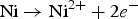
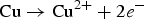
To clarify the corrosion mechanism of the ENIG-Cu system, research has focused on post-corrosion microscopic studies such as after long-term exposure to harsh natural climate [3,24] and harsh artificial environmental conditions [5,17,25 29]. Xiao et al. [3] investigated the corrosion behaviour of microporous ENIG-plated PCBs by exposing samples in the Turpan area of China for 24 months which has a harsh corrosive environment. By the post-corrosion analysis of the intermittently selected samples, they concluded that galvanic corrosion through the microporous surface of Au occurred through the following steps, (a) water condensation and dust sedimentation in the vicinity of the pores, (b) formation of corrosion product induced by galvanic coupling and (c) piling up of corrosion products reaching the surface. The proposed corrosion mechanism for the ENIG-Cu system exposed to the Turpan area is based on the high surface ratio of cathode-to-anode in which the cathodic reactions occurred at the Au surface (Equation (1)). The underlying layers of Ni and Cu act as an anode. The anodic reactions occur inside the micropores (Equations (2) and (3)).

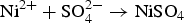
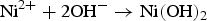
Subsequently, corrosion products can form by chemical reaction with dissolved polyatomic anions such as OH-,  and
and  (Equations (4)–(7)).


Murugan et al. [17] exposed a set of different stack configurations of Ni, Ni–P, and Au coatings with identical thicknesses to harsh artificial environments to investigate the corrosion mechanism for the ENIG-Cu system. They showed that multi-layered stack configuration, such as Ni–P/Ni/Au, Ni/Ni–P/Au, and Ni–P/Ni/Ni–P/Au, expedites corrosion due to having multiple interfaces enhancing galvanic corrosion as compared to that in the presence of a single layer of intermediate Ni-based materials such as Ni/Au and Ni–P/Au. On the other hand, Collins et al. [5] showed that multi-layered stack designs of electrical connector coatings, such as Ni/Ni–P/Au and Ni/Ni–Pd/Au, displayed better corrosion performance than Ni/Au and Ni–P/Au. They reported that the enhanced corrosion performance of the multi-layered stack design was attributed to the thickness of the multi-layered coating system, compactness of the Au layer with fewer defects, and reduction in the electrochemical potential difference between layers which alleviated the effect on local galvanic corrosion. In the research mentioned above, a post-mortem analysis approach was used to explain the corrosion mechanism for the ENIG-Cu samples.
Although many studies focused on the post-corrosion analysis of the ENIG-Cu system after long-term exposure to harsh corrosive media are available, to the authors’ knowledge, no prior research has adopted a step-by-step approach in terms of visualisation of the corrosion phenomenon toward elucidating the corrosion initiation and propagation mechanisms. To understand the corrosion process at the local level, local electrochemical techniques give a thorough insight into the spatial distribution of local anodic and cathodic reactions [30]. Scanning electrochemical microscopy (SECM) is a versatile local electrochemical technique that provides resolved electrochemical data from a confined region of interest of an immersed substrate surface. By operating the SECM in the feedback mode, a steady-state redox current can be measured in the region of the bulk solution. The measured steady-state current by hemispherical diffusion of the redox mediator is perturbed while approaching the scanning probe, called microelectrode to the proximity of the substrate. Negative feedback indicates a less electrochemical active area while positive feedback indicates the opposite. The resulting local current map obtained while operating at the feedback mode provides insight into the spatially-resolved local electrochemical activity of the surface [31 33].
In this research, we provide a fundamental understanding of the local corrosion behaviour of the ENIG-Cu system on metallic pins of SD memory cards in an acidic chloride-containing aqueous environment. The microstructural, compositional, electrochemical, and topographical characterisation of as-received samples were performed using scanning electron microscopy/energy-dispersive X-ray (SEM/EDS) spectroscopy, X-ray diffraction (XRD), atomic force microscopy (AFM) and open circuit potential (OCP) measurements. Focused ion beam (FIB), potentiodynamic polarisation (PDP) and SECM experiments provided quantitative and qualitative insight into the corrosion behaviour of the ENIG-Cu system. The FIB milling technique complemented the PDP information to study the corrosion attack morphology at various stages of the anodic polarisation. The local electrochemical activity of the ENIG surface after each polarisation step was investigated by the SECM operating in the feedback mode.
Experimental procedures
Material
The commercial SD memory cards were purchased from Coolblue Company (Dutch electronic commerce). The plastic holder of the SD card was removed to gain access to the inside PCB. The Cu pins inside PCB are coated with an ENIG final finishing. The dimensions of each pin are 2 mm × 4 mm. The schematic cross-sectional configuration of the ENIG system on a Cu substrate which is plated on a plastic backbone of the SD memory card is shown in Figure 1.
The schematic cross-sectional illustration of the ENIG-Cu system in the SD card (The width of each pin is approx. 2 mm; the thickness of each layer is not to scale for representative purpose).
Microstructural and compositional analysis
SEM/EDS
To study the morphology and elemental composition of the as-received and post-corroded samples, a scanning electron microscope (SEM) equipped with energy-dispersive X-ray spectroscopy (EDS) detector (Jeol JSM-IT100) was used. The top-view SEM/EDS data were collected at an accelerated voltage of 20 keV in collecting the emitted secondary electrons (SE) mode. For cross-sectional imaging of the entire thickness of the ENIG-Cu system, an as-received sample was embedded in an epoxy resin and subsequently ground to 4000 grit with SiC sanding paper. Afterward, the sample was polished with a fine diamond suspension (Struers DiaDua-2) with particle sizes of 3 and 1 μm. The sample was cleaned for 10 min immersed in isopropanol (IPA) using an ultrasonic bath (Emag Emmi 20HC) and dried with compressed air.
XRD
To study the crystallinity of the underneath Ni layer, XRD measurements were carried out. The Au top-layer of the as-received samples was ground with 4000 grit of SiC sanding paper to expose the underneath Ni layer. An X-ray diffractometer (Bruker D8 Advance) with Bragg–Brentano geometry and Lynxeye position-sensitive detector was used. Cu/Kα radiation and Ni filter were applied. The XRD measurement was carried out in the scan range (2θ) of 20-100°, with a step size of 0.03° and a dwell time of 1 s.
AFM
AFM was conducted on an as-received sample to characterise the surface topography. The AFM measurements were performed in the tapping mode using a Bruker Dimension Edge™ instrument with Nanodrive v8.05 software. Antimony (n) doped silicon cantilevers were used. AFM maps of 25 μm × 25 μm (XY plane) were performed at a scan rate of 0.4 Hz and a resolution of 256 × 256 points. To ensure the statistical significance of the data four map measurements at random locations were performed. The raw data were analysed using the open-source software Gwyddion v2.50.
PFIB
Plasma-focused ion beam (PFIB) microscopy was applied to investigate the cross-section of the as-received and post-corroded samples. A Thermo Scientific™ Helios™ UXe DualBeam G4 PFIB microscope was used. An accelerated voltage of 5 keV was set for surface imaging and 20 keV for the EDS measurements. Both are in the high-resolution SE mode. The blind mode for FIB sectioning was selected to preserve the surface and the ion-beam was used for the milling [34].
Electrochemical analysis
OCP and PDP
OCP and PDP measurements were used to determine the surface integrity of as-received samples and corrosion performance of the ENIG-Cu system in different pHs. The measurements were performed with a Biologic SP 300 multichannel potentiostat. A typical three-electrode cell consisted of Ag/AgCl electrode (sat. KCl) as a reference electrode, platinum wire as an auxiliary electrode, and the ENIG-Cu system as a working electrode. To prevent crevice corrosion from the edges of the backbone plastic, the ENIG-Cu sample (metallic pins) was masked with an adhesive sealing tape, and each pin's central part was exposed to the aqueous electrolyte. The exposed surface area was calculated before the experiments by using the ImageJ software.
OCP measurements of Au, Ni, and Cu were performed in an aerated 3.5 wt-% NaCl solution at pH 2. To measure the OCP of Au, a commercially pure Au flake was used and for the Cu and the intermediate Ni layer, a tilted abrasion of the ENIG-Cu sample was performed by SiC 2000 grit sanding paper to partly remove the Au layer and expose the Cu and the Ni (as shown in Figure S1). The OCP measurements were recorded during the 600s.
OCP and PDP measurements of the ENIG-Cu samples were performed in an aerated 3.5 wt-% NaCl at different pHs (2, 3, 4, 5 and 10). The pH adjustments of the solution were carried out by concentrated hydrochloric acid (HCl) for acidic solutions and concentrated NaOH solution for alkaline solutions with Milli-Q® ultrapure water at room temperature. Before the electrochemical measurements, the ENIG-Cu samples were cleaned in an ultrasonic bath (Emag Emmi 20HC) for 10 min during immersion in isopropanol and subsequently dried with compressed air. OCP values were stabilised to a steady-state response for 25 min. Then, PDP measurements were performed in the potential range from −0.15 V to 0.80 V (vs. OCP) with a scan range of 1 mV s−1. To estimate the corrosion potential (Ecorr) and the corrosion current density (icorr), Tafel extrapolation was applied using EC-Lab V11.33 software. At least three repetitions were carried out to check the level of reproducibility of the experiments. Sample preparation to study the different stages of corrosion evolution by SEM/EDS was done by the termination of the anodic polarisation measurements at seven anodic potentials: +40, +80, +130, +200, +320, +680, and +800 mV vs OCP. Then, the post-corroded samples after each stage of anodic polarisation were rinsed with Milli-Q® ultrapure water and dried with compressed clean air.
SECM
The post-corroded samples obtained after each step of the anodic PDP measurements were embedded in epoxy. An SECM instrument SCV370 model (Princeton Applied Research, AMETEK Inc.) was used. Scanning experiments operating in the feedback mode were carried out using 3.5 wt-% NaCl + 2mM ferrocenemethanol (FcMeOH) as a redox mediator. The SECM electrochemical cell consisted of a disc-shaped Pt-microelectrode of 10 μm diameter (by Sensolytics Inc.) as a working electrode, a platinum plate as an auxiliary electrode, and an Ag/AgCl, KCl (sat.) electrode as a reference electrode. During the experiments, the microelectrode was polarised at 0.5 V (vs. Ag/AgCl) to oxidise the mediator from Fe (II) to Fe (III). The sample remained at OCP conditions.
To establish the distance between the microelectrode and the ENIG-Cu surface before scanning, an approach curve of the SECM tip was measured. The tip–sample distance was fixed at 15 μm and a scan rate of 20 μms−1 was used. SECM scans were started after a resting time of 5 min after immersion before each scan.
Results and discussion
Microstructural and compositional characterisation of as-received ENIG-Cu samples
In Figure 2, microstructural, topography, and compositional analysis of the ENIG-Cu system are shown. The top-view SEM image of the metallic pin of the as-received SD memory card with the ENIG-Cu system (Figure 2(a)). It shows a heterogeneous topology with the presence of local defects. In addition, the topography map of the top-layer surface is presented in Figure 2(b). From the analysis of the topography map, the maximum valley depth (Sv) and root mean square roughness (Sq) values of the surface were 251 ± 38 nm and 72 ± 2 nm, respectively. Line 1 is a selected topography line scan from the topography map having the highest pit height (Figure 2(b)). The depth profile of Line 1 shows a sudden drop of the height, 151 nm, over a micro-defect, illustrated in the red dashed box in Figure 2(c). To gain more insight into the Au layer thickness at the trough of the selected micro-defect and the Au/Ni interface quality, FIB milling was performed on the same spot. In Figure 2(a), the red dashed line in the top-view SEM image of the selected micro-defect shows the plane of interest for FIB milling. The cross-sectional FIB-SEM image at the plane of interest is shown in Figure 2(d). A Pt layer was deposited to protect the Au layer from Xe damage while milling. The uneven topography of the Au layer shown in Figure 2(b) by AFM was corroborated by the cross-sectional FIB-SEM image (Figure 2(d)). The inset is the magnified view of the Au/Ni interface at the bottom of the micro-defect.
Microstructural, topography, and compositional analysis of the ENIG-Cu system. (a) Top-view SEM image of the ENIG-Cu system surface with a dashed line for the micro-defect indication, (b) AFM topography map of the ENIG-Cu system surface with a line for the micro-defect indication, (c) the line depth profile on the micro-defect, (d) the cross-sectional FIB-SEM image of the micro-defect, low and high magnification and (e) the polished cross-section of the sample for compositional analysis of each layer. EDS points analysis of (f) Au top-layer (g) intermediate Ni layer and (h) the Cu substrate.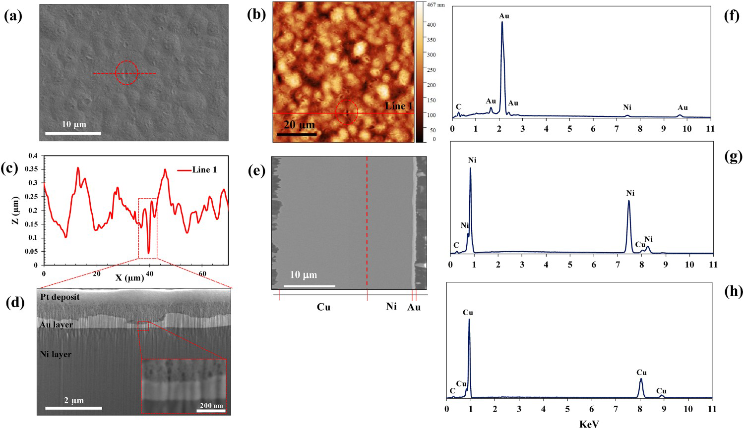
Furthermore, to perform a compositional study of each layer, a cross-sectional SEM image of the whole ENIG-Cu system is shown in Figure 2(e). Point EDS analyses provided the element compositions of each layer from top to bottom. The spectra are presented in Figure 2(f–h). Also, the thickness of the whole metallic pin attached to the plastic board is 27.0 ± 1.4 μm. The thickness of the ENIG-Cu layers is 15.7 ± 0.9 μm of Cu, 10.5 ± 0.5 μm of Ni, and 408 ± 127 nm of top-layer Au. Finally, XRD measurements of the intermediate Ni layer were carried out. The XRD pattern is shown in Figure S2. The results demonstrate that the intermediate layer consisted of pure Ni with a nano-crystalline structure. By considering the thickness and the Sv values on the Au top-layer, the micro-defects can be regarded as superficial, and they do not reach the underneath Ni layer.
A cross-sectional FIB-SEM image of the selected micro-defect showed that a thin layer of the protective Au layer, with a thickness of 186 ± 27 nm, is present on the intermediate Ni layer. Also, the flat Au/Ni interface shows that the uneven surface of the top-layer is not due to the surface quality of the Ni layer. Therefore, the bottom of the deepest micro-defect where the thinnest thickness of the Au layer covers the Ni substrate might be a location of high porosity. The relative amount of ‘empty’ volume or that of exposed substrate area is considered the porosity of a layer. The porosity level of the Au top-layer is inversely correlated to the thickness [35].
The spectrum for the Au top-layer (Figure 2(f)) shows Au-peaks as the dominant element and a minor peak corresponding to the Ni. The detection of Ni may be explained by the thin layer of the Au layer and the significant interaction volume of the incident electron beam [36]. The spectrum corresponding to the intermediate layer showed mainly peaks attributed to Ni (Figure 2(g)). A phosphorous signal around 2 keV energy [37] was not detected. This element is typically a constituent of the electroless Ni layer. In Figure 2(h), the spectrum of the substrate layer is shown. The main element detected is Cu as expected. Minor peaks corresponding to C are found in all spectra (Figure 2(f–h)) which can be attributed to organic contamination.
Electrochemical study of as-received samples
The corrosion properties of the ENIG-Cu sample were studied by PDP experiments. The behaviour of the sample was studied in 3.5% NaCl solutions at different pHs ranging from 2 to 10. Representative curves at each pH are shown in Figure 3. The cathodic process is under activation polarisation control. The anodic branches show relatively high anodic activity even at low overpotentials. At acidic pHs, higher overpotentials result in a stable, relatively high anodic current density indicating the absence of passivation behaviour [38]. In pH 2, the polarisation curve reaches a limiting current density of 9.59 ± 1.40 mA cm−2. On the other hand, active/passive behaviour in the anodic curve of the ENIG-Cu system at an alkaline pH of 10 is shown. The intact surface of the ENIG-Cu system at basic pH of 10 after anodic polarisation was shown in Figure S3.
PDP curves for ENIG-Cu sample in 3.5% NaCl solution at different pHs.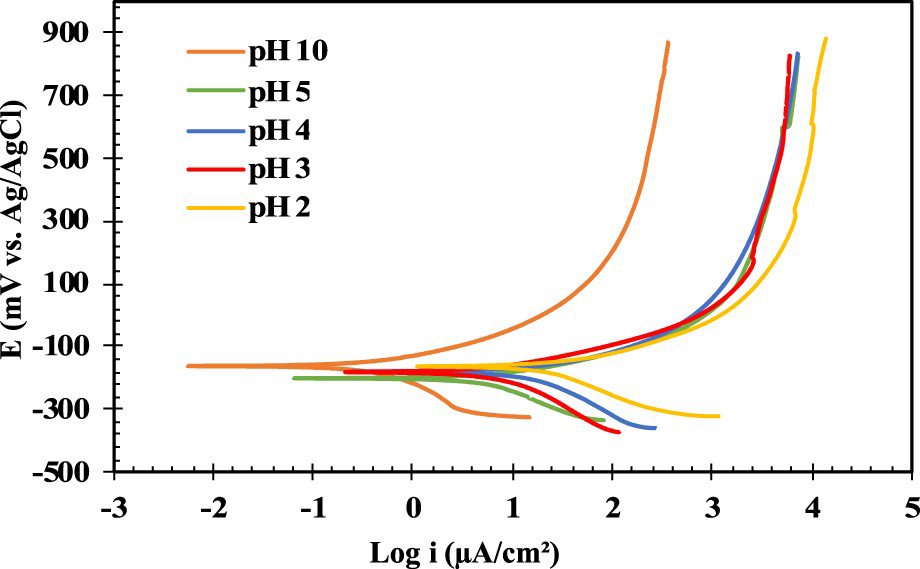
In Figure 4(a, b), the average values of corrosion current density and corrosion potential extrapolated from the polarisation curves are presented, respectively. The corrosion current densities in acidic pHs are higher than in alkaline pH 10. For pH 10 and based on the Pourbaix diagram [39] passivity of the Ni and Cu is expected, with the presence of stable (hydr)oxides such as Ni(OH)2, and Ni3O4. Nevertheless, the high concentration of chloride species and the presence of porosity limits their stability leading to localised activity related to the high anodic activity, also at low overpotentials, observed in the polarisation curves. The corrosion potential values do not differ significantly, as shown in Figure 4(b). The highest corrosion potential is –175 ± 20 mV for pH 3 and the lowest corrosion potential is –216 ± 19 mV for pH 5.
The effect of solution pH on corrosion behaviour of the ENIG-Cu system: (a) corrosion current density vs. pH and (b) corrosion potential vs. pH.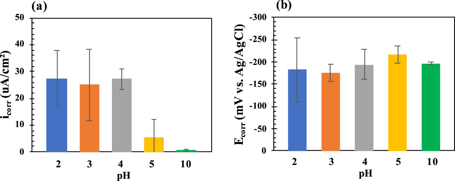
To further analyse the corrosion mechanism of the ENIG-Cu sample, further studies were conducted in the acidic solution of pH 2. From the SEM/FIB and AFM analysis in Figure 2, the presence of micro-defects facilitating the exposure of the underneath Ni through the possible porosities was hinted. To confirm the presence of defects in the outer Au layer exposing the Ni underneath, OCP measurements were carried out for three different sample types: pure Au flake, intermediate Ni layer, and as-received ENIG-Cu sample.
OCP measurements in 3.5 wt-% NaCl at pH 2 are shown in Figure 5. During the measurements, the potential values of the Au flake and Ni layer remained relatively stable with minor changes. The potentials of Au and Ni were 304 ± 20 mV and –142 ± 37 mV at time zero, respectively. The initial OCP value of 162 mV ± 43 mV of the as-received sample laid between the potentials of the Au and Ni layers. After a short time, the OCP value of the sample decreased to −147 mV± 49 mV and approached the potential values of the Ni layer. This might be an indication that the Ni was exposed from the early stages of exposure in the as-received sample. However, the defects on the Au layer conducting the corrosive solution to the underneath Ni were not detected by cross-sectional FIB milling in Figure 2(d). The presence of imperfections in the Au top-layer which expose bare Ni to air is normally attributed to flaws during the fabrication process. For instance, Monlevade et al. [28] showed that evaporation of trapped impurities during the immersion gold process leaves behind a cavity in the top-layer of the ENIG-Cu system.
The OCP values of Au flake, Ni layer and as-received ENIG sample in 3.5 wt-% NaCl at pH 2.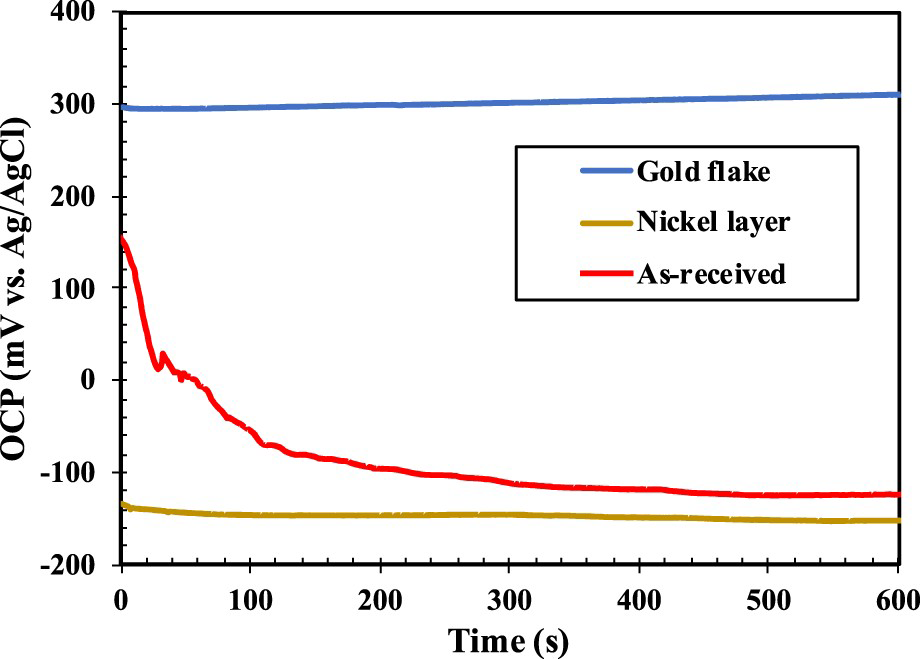
Microstructural and electrochemical characterisation of post-corroded ENIG samples
To comprehensively elucidate the ENIG surface's corrosion mechanism in the aqueous acidic media, PDP measurements for the ENIG surface in 3.5 wt-% NaCl solution at pH 2 were terminated at different anodic potentials: +40, +80, +130, +200, +320, +680, and +800 mV vs OCP. The surface of the sample was analysed by SEM/EDS after each applied potential.
In Figure 6, the top-view SEM/EDS pit analysis of ENIG samples at the selected three potentials in the anodic polarisation is shown (+80, +200, and +800 mV vs OCP). The SEM/EDS analysis of the rest of the potential stages is presented in Figure S4 for completeness. The SEM images of the overall surface of post-corroded samples after the termination of the PDP measurements at the selected three potentials are shown in Figure S5. After anodic polarisation until 80 mV, one circular pit was formed and the rest of the surface was intact. As shown in Figure 6(a), inside the circular pit, only Ni is detected from the EDS mapping analysis. Figure 6(b) shows the SEM/EDS images of the surface after anodic polarisation until 200 mV (vs OCP). Five circular pits were formed in the overall exposed sample to the solution and the rest of the surface was intact. The pit mouth diameter was not significantly different from the sample polarised to +80 mV (Figure 6(a)). Pits now reached the underneath Cu layer as well. The presence of Ni inside the pit is reduced. The final stage, anodic polarisation until 800 mV, is shown in Figure 6(c). Seven circular pits were formed in the overall exposed sample surface and the rest of the surface was intact. Two major circular pits with a larger mouth diameter and five minor pits. The localised attacks are now significantly more extensive and the intermediate Ni layer is completely gone.
The top-view SEM image and EDS elemental maps for pit analysis of ENIG samples in 3.5% NaCl – pH2, after anodically scan polarisation until the following potentials: (a) 80 mV, (b) 200 mV and (c) 800 mV.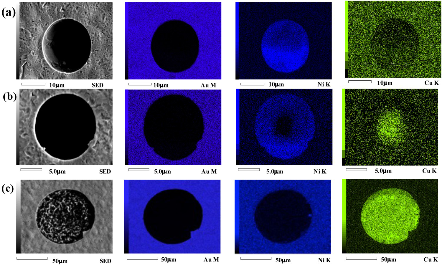
After anodic polarisation until 80 mV (vs OCP), the lack of Cu signal inside the pit shows that the localised corrosion was confined to the Ni. At the beginning of the anodic polarisation, the local corrosion of the Ni is assumed to initiate from an existing breach. With the elliptical dissolution of the Ni, whenever a sufficient amount of the Ni is depleted, the loose lid of the undercut top-layer Au would be detached to leave a circular shape of the pit mouth. The autocatalytic nature of pitting growth coupled with the surface imperfections provides a high ratio of cathode-to-anode surface to propagate the pitting process. Pits are not formed all simultaneously; some are earlier than others, depending on local electrolyte and surface (defect) conditions [17]. After anodic polarisation until 800 mV (vs OCP), the high potential polarisation resulted in the intensive dissolution of the Ni layer not only reaching the underlying Cu substrate but also propagating in the near-surface area.
The surface morphology analysis shows that a loose circular Au layer is removed from the surface to the solution after the extensive dissolution of the underneath Ni. Since the removal of the loose lid of the Au top-layer is also dependent on the mechanical strength of the Au layer at that specific region, the detachment can happen already in the early stages of polarisation. In Figure 7(a), due to the dissolution of the underneath metallic layer, a circular dent represents a loose lid of top-layer Au with a void underneath after anodic polarisation until 320 mV (vs OCP). A mechanical force was applied to remove the loose lid by manually peeling off a plastic tape from the surface. In Figure 7(b), the detachment of the open circular lid of the Au top-layer due to applied mechanical force from the same pit is shown.
(a) The loose circular lid of top-layer Au with a void underneath, before applying the mechanical force of tape peel-off after anodic polarisation until 320 mV (vs OCP) and (b) the same pit after the tape peel-off.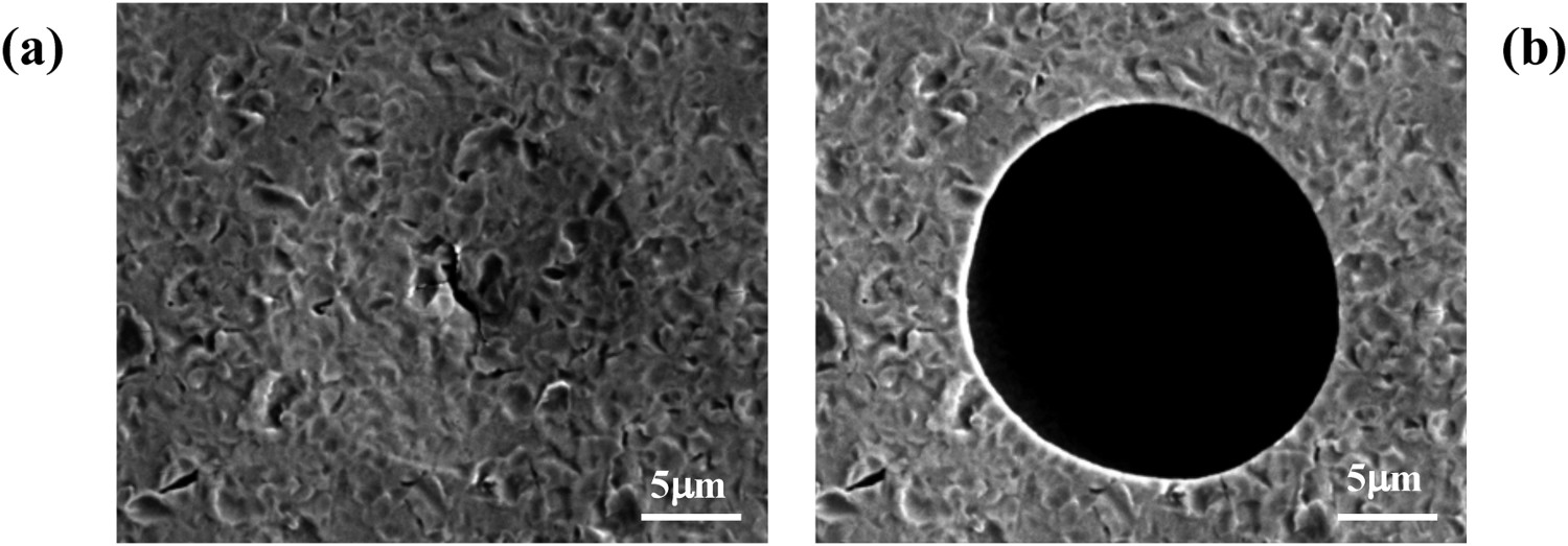
Cross-sectional and top-view FIB-SEM analyses of the pits detected at the different potentials are shown in Figure 8. The cross-section analysis for the sample polarised to 80 mV Figure 8(a) shows an elliptical shape of the pit growth confirming that the general dissolution direction of Ni was a combination of lateral and in-depth. However, the bottom of the pit does not reach the Ni/Cu interface. In Figure 8(b), the cross-section of the pit of the sample polarised to 200 mV as the middle stage is shown. The ternary system of Au/Ni/Cu was exposed to the corrosive solution and the large undercutting region, compared to the initial stage, was formed in the Cu layer. Although the direction of the localised corrosion is a combination of the lateral and in-depth, the contribution of the lateral propagation is slightly bigger than the in-depth propagation. The elliptical growth pattern of the undercutting region in the Cu layer leaves a spiky surface for the Cu layer. The morphology of a major pit on the post-corroded ENIG surface after the final stage of the anodic polarisation, i.e. after 800mV anodic polarisation, is shown in Figure 8(c1–c3). The dominant lateral corrosion propagation direction led to the formation of a significantly larger circular pit with an average diameter value of 154.0 ± 70.1 μm, showing a wide variation in pit mouth size distribution. In Figure 8(c2), the shallow dent in the centre of the pit is shown showing the Cu dissolution. The in-depth direction of the corrosion in the Cu layer was limited as the lateral growth of corrosion in the Ni resulted in a large pit mouth diameter. The Ni/Cu interface at the edge of the pit shown in Figure 8(c3) demonstrates the lateral corrosion growth.
The cross-sectional and top-view FIB-SEM/EDS pit analysis of ENIG samples in 3.5% NaCl at pH 2: (a) after 80 mV anodically PDP, (b) after 200 mV anodically PDP, (c1) top-view SEM image after 800 mV anodically PDP, (c2) tilted top-view SEM image from inside the pit after 800 mV anodically PDP and (c3) cross-sectional view of the pit edge after 800 mV anodically PDP.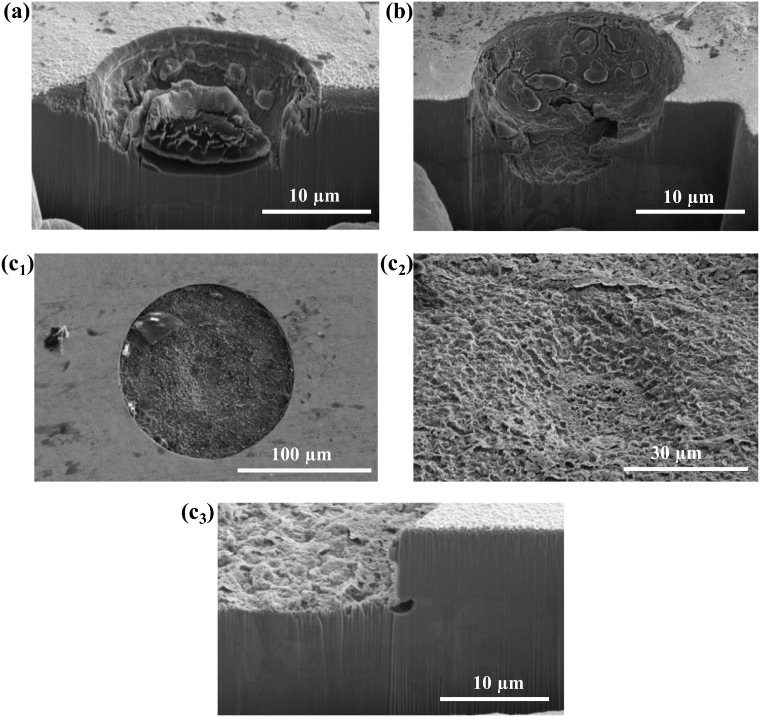
In the initial stage, the galvanic coupling of the Ni as an anode with a small surface area and the Au as a cathode with a large surface area led to the fast dissolution of the Ni. The high ratio of cathode-to-anode surface provides a high galvanic driving force for the localised corrosion of the Ni with a high local anodic current [16]. The anodic reaction for the Ni dissolution is expected as Equation (2) [3,26]. Owing to the nano-crystalline structure of the Ni, the exposed Ni in the pit contains a high concentration of grain boundaries that may act as structural discontinuity. These microstructural heterogeneities might contribute to the inferior corrosion performance of the Ni [5]. Owing to the acidity of the solution, the possible reduction reaction on the Au surface is expected to be according to Equation (8).

Local electrochemical study of post-corroded samples by SECM
To study the local electrochemical activity of the post-corroded ENIG surface after the initial, middle, and final stages of anodic polarisation, SECM measurements in the feedback mode were performed. Because of the conductive nature of the Au top-layer, a positive feedback approach curve was obtained when the microelectrode was approaching the ENIG surface, as shown in Figure S6. In the positive feedback approach curve, due to the active electrochemical behaviour of the substrate in terms of the regeneration of the redox species, the tip current increases dramatically by approaching the surface in the close vicinity of the substrate [45]. The SECM normalised (normalised current = i/ilimit) maps in the positive feedback mode are shown in Figure 9. Owing to the small diameter of pit mouths in the initial and the middle stages, scan areas of 400 μm × 400 μm were mapped, Figure 9(a, b); however, for the final stage of the anodic polarisation, a relatively large scan area of 800 μm × 800 μm, Figure 9(c), was chosen to cover the whole area of the pit mouth. The normalised current on the pit from the initial stage of anodic polarisation to the final stage was diminished. In Figure 9(a), the SECM normalised current map of the post-corroded surface of ENIG after 80mV of anodic polarisation showed the active site with an intense peak at the pit location. During the middle stage of the anodic polarisation, the pit mouth remains almost the same as the initial stage but the in-depth growth of the pit led to exposing the Cu layer to the solution. Therefore, due to the higher distance between the surface at the bottom of the pit and the SECM tip, the peak intensity at the active sites of the middle stage is abated, as shown in the SECM normalised current map, Figure 9(b). At the final stage of polarisation, as shown in Figure 9(c), the size of the pit mouth was enlarged, and the pit was deeper due to the complete dissolution of the intermediate Ni layer. In Figure 9(c), the size of the active site corresponds to the large pit mouth and the low intensity of the normalised peak is due to the high distance of the gap between the surface at the bottom of the pit and the SECM tip.
The SECM pit analysis of ENIG-Cu samples in 2mM FcMeOH, 3.5% NaCl at pH 2 after the anodic polarisation until (a) 80 mV (b) 200 mV and (c) 800 mV.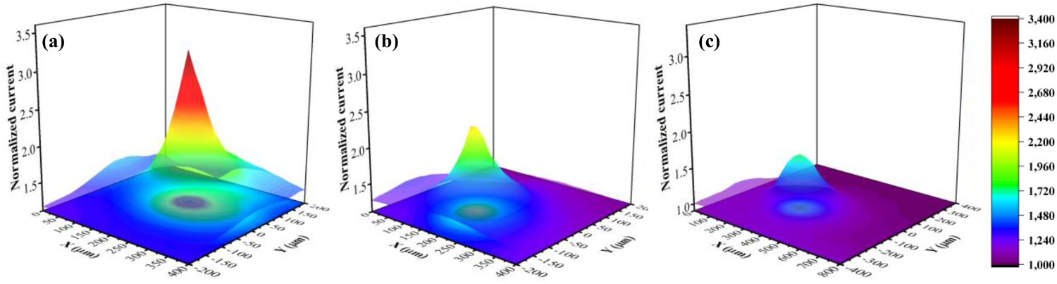
Corrosion mechanism of ENIG samples with micro-defects
The results from the morphological and electrochemical experiments have shown that the as-received ENIG-Cu system contains some micro-defects that exposed the bare Ni to corrosive media. The imperfections of the Au top-layer provide the preferred location for the initiation of the localised corrosion attack. A schematic cross-sectional sketch of the first step of localised corrosion attack from a pre-existing micro-defect as the corrosion initiation location is shown in Figure 10(a). To initiate the localised corrosion attack, a high cathode-to-anode surface area ratio was provided by the micro-defects. In the next step of the anodic polarisation, the elliptical dissolution of the Ni shows that the direction of the dissolution is a combination of lateral and in-depth pit growth. By progressive elliptical dissolution of the Ni, the Au top-layer is undercut and the thin Au layer shows a dented morphology from a top-view, Figure 10(b). With further undercutting of the Au top-layer, the loose Au cap is detached to open the pit, Figure 10(c). It must be mentioned that detachment of the loose lid may happen in either earlier or later steps due to the Au layer's mechanical properties, which are determined by the surface texture of the top-layer surface. As shown in Figure 10(a–c), until reaching the Ni/Cu interface, the direction of the Ni dissolution is governed by an elliptical dissolution morphology which results in an increasingly widening and deepening of the pit. As shown in Figure 10(d), as soon as the Cu is exposed to the corrosive media, the limited elliptical dissolution of the Cu occurs due to the acidic and highly Cl− concentrated solution at the bottom of the pit. Subsequently, the rate for Cu dissolution remains limited and the corrosion attack direction tends to show lateral growth in the Ni layer, Figure 10(e). Eventually, in Figure 10(f), the post-corroded surface of the ENIG-Cu system after the final stage of the anodic polarisation leaves a large hole with a small dent in the middle of the hole at which the Cu was slightly corroded.
Schematic illustration of step-by-step localised corrosion of ENIG-Cu samples in 3.5% NaCl at pH 2 by PDP, (a–c) progressive dissolution of the Ni in a combinational direction of lateral and in-depth, galvanic couple of Au/Ni, (d–f) progressive dissolution of the Ni in a lateral direction and marginal dissolution of the Cu in an in-depth direction, the ternary system of Au/Ni/Cu (The thickness of each layer was exaggerated for representative purpose).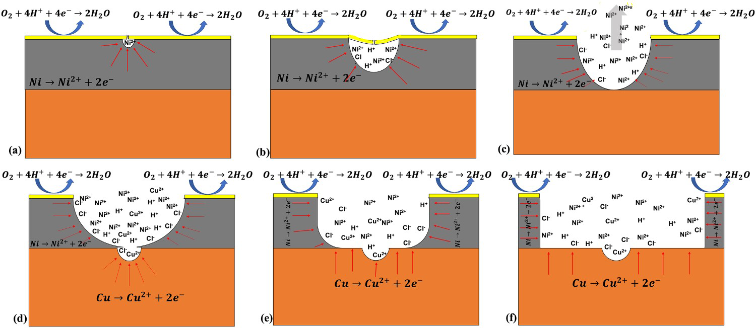
Conclusions
This study aims to show a fundamental understanding of the localised corrosion mechanism of an as-received ENIG-Cu system of an SD memory card in an acidic chloride-containing aqueous environment. The applied step-by-step methodology, in terms of visualisation of the gradually progressing corrosion phenomena, based on a combination of microscopic, analytical, and electrochemical measurements enabled the illustration of the localised corrosion evolution. It was revealed that some micro-defects were present in the Au top-layer as imperfections. Exposing the Ni layer through these micro-defects led to local galvanic corrosion of the ENIG-Cu system which was governed by the high ratio of Au-to-Ni, cathode-to-anode, and surface area. The high driving force of galvanic corrosion for the Au/Ni couple caused the relatively fast and sustained dissolution of the Ni. The elliptical dissolution of the Ni, a combination of lateral and in-depth pit growth, continued to reach Ni/Cu interface. Then, the Ni dissolution direction changed to lateral growth after a relatively limited elliptical dissolution of the Cu. In the ternary system of Au/Ni/Cu, the corrosion rate of Ni compared to Cu was considerable. It was concluded that the direction of the metallic dissolution has changed during the corrosion evolution due to the pit geometry and the exposed materials with time.
Footnotes
Acknowledgements
The authors thank Mr. Ziyu Li for assisting with the SECM measurements.
Disclosure statement
No potential conflict of interest was reported by the author(s).