
Abstract
We developed cost-effective and high-throughput techniques to fabricate metal nanostructure arrays of various geometries on solid substrates. Surface plasmons of these nanostructure arrays were investigated both experimentally and theoretically. We systematically studied the effects of different parameters on the localized surface plasmon resonance of the nanostructure arrays. We further developed a few approaches to tailor surface plasmons for different applications. As an example of the applications of these nanostructure arrays, we demonstrated all-optical plasmonic switches/modulators based on long-range ordered Au nanodisk arrays and photoresponsive liquid crystals. The advantages of such arrays include low-cost, high-throughput, and tailorable plasmonic properties. These arrays can serve as a platform that will stimulate further progress in both fundamental research and engineering applications of plasmonics.
Keywords
Introduction
Plasmonics, an emerging branch of nanophotonics, concerns properties of collective electronic excitations (known as surface plasmons) in films or nanostructures of noble metals (especially Au and Ag). 1,2 Based on the interactions between light and conduction electrons at the metal thin films or in the metal nanostructures, the surface plasmons lead to near-field localization of the light into subwavelength dimensions. 3 The strong spatial localization of light enables many important applications of surface plasmons: nanophotonic devices and circuits; 4 -9 molecular-specific biological sensing, imaging, and photothermal therapy; 10 -15 nanolithography; 16,17 surface plasmon tweezers; 18,19 and metamaterials. 20 -24 The surface plasmon-based nanophotonic circuits can carry optical and electric signals through the same thin metal circuitry. This feature makes it possible to combine the superior technical advantages of both photonics and electronics, and allows very large-scale electronics and photonics integration (VLSEPI). In another application, surface plasmon tweezers can operate with much less power than that of conventional optical tweezers, due to the high localization of the electromagnetic energy at the plasmonic nanostructures. Surface plasmon tweezers of a two-dimensional (2D) configuration can be easily integrated into microfluidic systems for the development of “lab-on-a-chip” technology. 19
In the above-mentioned applications, the fabrication of metal nanostructures represents the first and one of the most significant challenges. Flexible nanofabrication and nanoengineering techniques are often required to produce metal nanostructures with tunable plasmonic properties (e.g., the dispersion relation, resonance frequency, and bandwidth). Traditionally, metal nanostructures are prepared by the controlled precipitation and concurrent stabilization of incipient colloids. 25 -27 The resonance frequency and bandwidth of the localized surface plasmon resonance (LSPR) of such nanostructures are highly sensitive to their shape and size. This sensitivity has fostered research in the fabrication of metal nanostructures with different geometries (e.g., rods, rings, prisms, cubes, shells, and rice grains). 25,26,28 –33
Aside from colloidal nanoparticles in suspensions, ordered metal nanostructure arrays immobilized on solid substrates are of interest for applications such as nanoscale wave guides, surface-enhanced Raman spectroscopy (SERS), and biosensors. 27 The interest in the immobilized nanoparticles arises from several advantages unique to the nanoparticle arrays: easy control of interparticle spacing and position, which allows control of the plasmonic properties; no capping agents or stabilizers required (in contrast with colloidal nanoparticles), making the arrays ready for surface functionalization; and repeated use of the nanoparticles by releasing the absorbed or bounded substances from previous experiments. 27 The metal nanostructure arrays exhibit an additional shift of resonance frequency and change of bandwidth as a result of near-field or far-field coupling effects. The changes allow further tailoring of the plasmonic properties. 34 -38
We present our recent developments in fabrication, nanoengineering, and applications of various metal nanostructure arrays. By extending conventional nanosphere lithography (NSL), 39,40 we established new procedures that can produce nanostructures of more shapes and sizes on solid substrates. Compared with conventional lithography techniques such as photolithography, electron beam (e-beam) lithography, and focused ion beam lithography, 3,41 our self-assembly techniques have the advantages of low cost and high throughput when producing nanostructures with comparable or better plasmonic properties. Further, nanoengineering approaches were developed to tailor the plasmonic properties of the nanostructure arrays to meet the requirements of different applications. Effects of the engineerable parameters, like shape, size, and refractive index of surroundings, on the LSPR of the nanostructure arrays were investigated both experimentally and theoretically. Finally, all-optical active plasmonic switches/modulators were demonstrated as one of many applications using the nanostructure arrays.
Fabrication Techniques
By using NSL, we have produced three kinds of long-range ordered Au nanostructure arrays: nanoprisms, nanodisks, and nanoholes.
Au Nanoprism Arrays
Ordered Au nanoprism arrays were fabricated on glass substrates using conventional NSL, where monolayers of monodisperse polystyrene (PS) nanospheres acted as masks for the evaporation of Au (Fig. 1a). The glass substrates were pre-cleaned by immersion in piranha solution (H2SO4:H2O2 = 3:1) at 80 °C for 30 min, then rinsed with deionized (DI) water and dried with N2 gas. To enhance the adhesion between the Au and the glass substrates, a thin layer of Cr was used between them. Au nanoprisms were produced on the substrates after selective removal of PS nanospheres by toluene with ultrasonics.
There are several methods to produce close-packed monolayers of nanospheres on substrates, including spin coating, dip coating, and lift-up. 42 Figure 1b shows an Au-coated, 2-in. silicon wafer cut in half. There is a monolayer of nanospheres on its right half. The uniform color contrast between the two pieces of wafer indicates that the monolayer was uniform at a large scale. A lift-up method was used to produce the monolayer, and the detailed procedure is as follows. 43 (a) The substrate was placed at the bottom of a Petri dish filled with DI water. (b) PS nanospheres (10 wt%, Bangs lab) were mixed with the same volume of ethanol. (c) Mixture (200 μL) was slowly applied to the water surface by a pipette; a monolayer of nanospheres then appeared on the water surface. (d) A surfactant, sodium dodecyl sulfate of 2 wt% concentration, was used to drive the nanospheres into a close-packed monolayer. (e) The aqueous mixture in the Petri dish was drained, causing the monolayer to transfer onto the substrate surface.
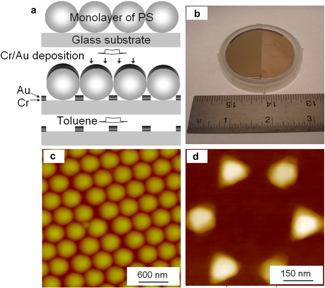
(a) Schematic of fabrication process for producing ordered Au nanoprism arrays on a glass substrate; (b) photograph of Au-coated, 2-in. silicon wafer cut in half. There is a monolayer of nanospheres on its right half, and the left half is a bare Au surface; (c) zoomed-in atomic force microscopy (AFM) image of a monolayer of nanospheres from (b); (d) AFM image of a Au nanoprism array immobilized on the glass substrate.
Figure 1c shows the atomic force microscopy (AFM) image of a monolayer of nanospheres with a mean diameter of 300 nm. The close-packed nanospheres were hexagonally arranged, with triangular interstices formed between every three neighboring spheres. Through the interstices, evaporated Au was deposited onto the substrates, forming Au nanoprisms (Fig. 1d). The size and shape of the nanoprisms could be controlled by tuning the amount of evaporated Au or the size of the nanospheres.
Au Nanodisk Arrays
The shapes of nanostructures produced by conventional NSL are limited to triangles and hexagons. 44 These shapes are based on the deposition of materials through, respectively, monolayers and double layers of close-packed nanospheres. Recent developments in NSL have enabled the fabrication of nanostructures of different shapes. 45 -56 We produced ordered Au nanodisk arrays by combining NSL with two-step reactive ion etching (RIE).
Figure 2a is a schematic of the nanodisk fabrication process. A monolayer of close-packed PS nanopheres was formed on an Au-coated glass substrate. Successive O2 RIE and Ar RIE (Plasma-Therm 720) morphed the monolayer into an array of separated nanoellipses, and selectively etched a portion of the Au and Cr film that was not protected by the nanoellipses. Ordered Au arrays were produced on the substrates after removing the remaining PS.
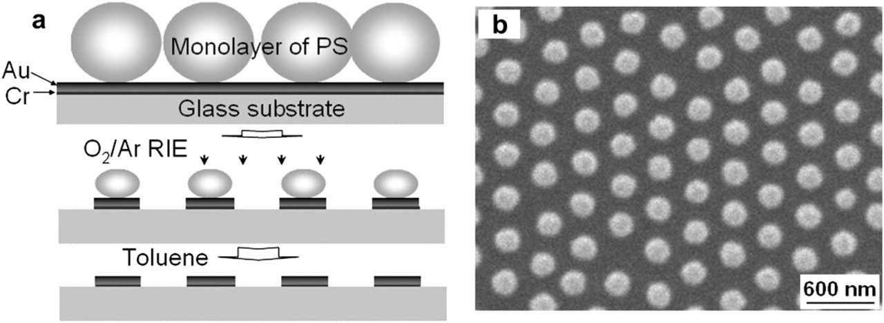
(a) Schematic of fabrication of ordered Au nanodisk arrays on a glass substrate; (b) scanning electron microscopy image of hexagonally arranged Au nanodisk arrays on a glass substrate.
Figure 2b shows a scanning electron microscopy (SEM) image of hexagonally arranged Au nanodisk arrays on a glass substrate. The arrays' period was 320 nm as determined from the SEM image; this measurement was consistent with the initial diameter of the nanospheres. In O2 RIE, the parameters included an etching time of 30 s, 20 sccm (Standard Cubic Centimeters per Minute) gas flow, 100 mTorr pressure, and 300 W power density. The same parameters were used in Ar RIE, except that the etching time was 100 s. The mean disk diameter was tuned by changing the O2 RIE time or power. In addition, by choosing PS nanospheres of different diameters, the period of the nanodisks was also tuned.
Nanohole Arrays in Au Thin Films
The plasmonic properties of nanohole arrays in metal films have generated a considerable amount of interest, because such films exhibit extraordinary optical transmission that has potential applications in optical filters, switches, displays, and sensors. 5,57 We combined NSL and O2 RIE to fabricate long-range ordered nanohole arrays of various sizes in Au thin films on substrates. Figure 3a is a schematic of the fabrication process. First, a monolayer of loosely packed nanoellipses was produced by O2 RIE of a monolayer of close-packed PS nanospheres on the substrate. Cr and Au were then sequentially deposited onto the sample using e-beam evaporation. The Cr/Au covered PS nanoellipses were selectively removed by ultrasonic agitation in toluene. This left nanohole arrays in the Cr/Au thin films.
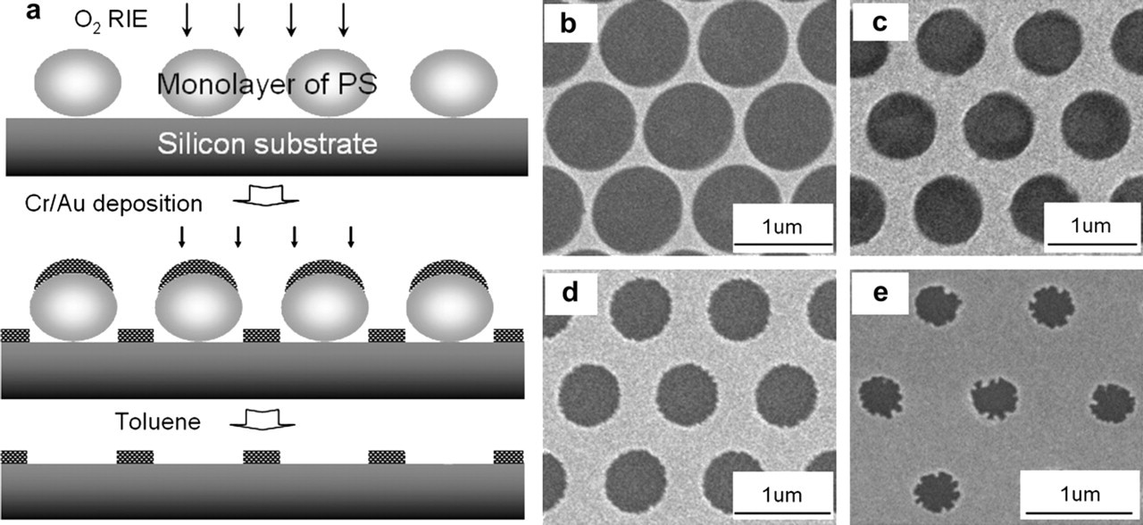
(a) Schematic of fabrication of nanohole arrays in a Au thin film on a silicon substrate; (b–e) scanning electron microscopy images of the hexagonally arranged nanohole arrays in Au thin films, with O2 reactive ion etching times of 3, 6, 8, and 11 min, respectively.
Figure 3b-e are SEM images of the nanohole arrays after 3, 6, 8, and 11 min, respectively, of RIE (Oxford RIE II Etcher) (in O2 gas at 20 sccm, at 15 mTorr, and at a power density of 100 W). The original PS spheres had a diameter of 1 μm; 5 nm Cr and 30 nm Au were deposited. When the longer RIE was applied, the internal sidewalls of the smaller holes were roughened due to the rougher PS surfaces (Fig. 3e). 55,56 The period of the holes was tuned by using PS spheres of different sizes.
Nanoengineering of Surface Plasmons
Rapid progress in plasmonics has led to many different applications of metal nanostructures. 19,27,58 -61 To achieve optimal performance for each application, the surface plasmon properties such as resonance frequency, intensity, and bandwidth must be tailored. For example, plasmon-enhanced solar cells have a higher energy conversion efficiency than that of conventional solar cells when the plasmon resonances overlap with the solar spectrum. 62 Plasmonic integrated circuits interfacing with optical fibers should have their plasmonic nanostructures optimized to achieve low loss and high spatial confinement of surface plasmon polaritons at the fiber window wavelength of 1.3 or 1.55 μm (as measured in vacuum). To minimize signal loss in biological sensing and imaging, surface plasmons of resonance wavelength in the biological window (700–1100 nm) are preferred. The highest enhancement factor in SERS was achieved when the resonance frequency of surface plasmons in the substrates was between the frequency of the excitation laser and the emission frequency of the molecules. 63
Both theoretical and experimental studies revealed that the properties of surface plasmons depend on multiple parameters, including shape, size, and composition of metal nanostructures, and dielectric constant of the media surrounding metal nanostructures. 1 We developed nanoengineering approaches for tailoring one or more parameters of the nanostructure arrays. The effects of individual parameters on the surface plasmons were studied experimentally, and analyzed theoretically through discrete dipole approximation (DDA) calculations. Two different nanostructures were examined: Au/TiO2 core/shell nanoprism arrays and Au nanodisk arrays.
Au/TiO2 Core/Shell Nanoprism Arrays
Metal nanostructures can be coated with an additional layer of a different material (metal, dielectric, or semiconductor) to form core/shell structures. A suitable choice of coating offers several advantages such as high tunability of surface plasmons and enhanced biocompatibility. The biocompatibility is essential for applications such as drug delivery and therapy. We produced Au/TiO2 core/shell nanoprism arrays by depositing conformal TiO2 shells onto the surfaces of the Au nanoprisms (Fig. 1d). With a high refractive index that depends on the crystal structure, TiO2 is a commonly used optical material. 64 Recently, photocatalytic properties and reversible tuning of LSPR have been observed in Ag/TiO2 core/shell colloids. 65,66
At room temperature, we deposited TiO2 shells of controlled thickness in an atomic layer deposition (ALD) system that we constructed. 67 The setup consisted of a stainless steel chamber equipped with a liquid N2 trap and a mechanical pump. The base vacuum of the chamber was about 5 × 10⁻⁴ Torr. The samples were repeatedly and alternatively exposed to two precursors, TiCl4 and H2O. The exposure time for both precursors was < 5 s, and the intervals between two exposures were 30 s to let the chamber recover to the base vacuum. In the half-cycle of the process, TiCl4 vapor reacted with hydroxyl species on the sample surfaces. In the following half-cycle, the resulting –TiClx groups reacted with H2O vapor and developed into –Ti(OH)x groups (1 ≤ × ≤ 3), the condensation of which resulted in a TiO2 layer. A deposition rate of 1.8 Å per cycle was observed. Figure 4a shows a schematic of the conformal TiO2 layer on the exposed surfaces of the Au nanoparticles. The thickness of TiO2 was controlled by the number of cycles. We observed the effects of TiO2 thickness on the LSPR of nanoprism arrays (Fig. 4b). The nanoprism arrays were thermally annealed (details in the followed part of this section) before the deposition of TiO2 to enhance the resonance. The ex situ extinction spectra recorded from the arrays exhibited a continuous redshift of the resonance peak (identified as in-plane dipole resonance 68 ) with an increase of TiO2 thickness. The redshift arose from an increase in the average refractive index of the Au nanoprisms' surroundings when the replacement of air by TiO2 occurred on the exposed prism surfaces. The peak position remained unchanged when the thickness of TiO2 was increased beyond the characteristic electromagnetic field decay length of the nanoprisms.
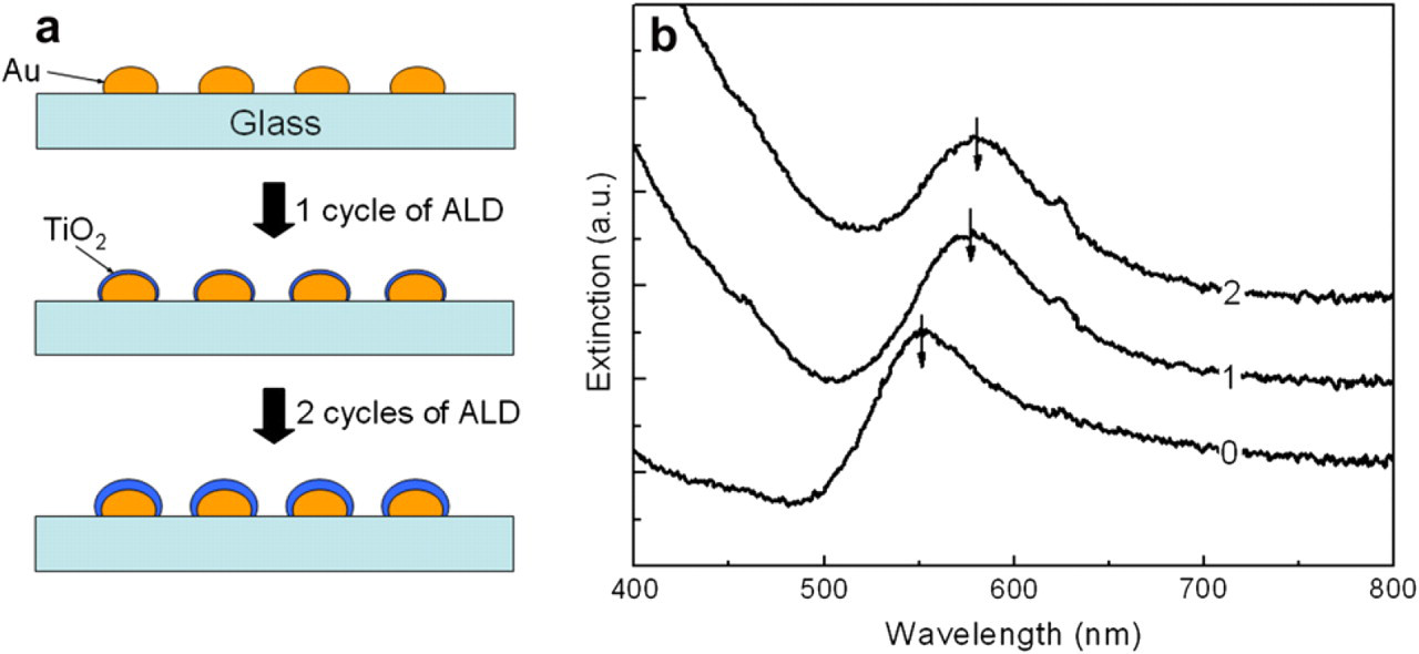
(a) Schematic of atomic layer deposition (ALD) process for formation of TiO2 shells on the exposed surfaces of Au nanoparticle arrays immobilized on the glass substrate; (b) measured extinction spectra of annealed Au nanoprism arrays after different cycles of ALD deposition of TiO2.
To further engineer the LSPR of the core/shell nanoprism arrays, thermal annealing processes were carried out in a furnace under ambient conditions, at a series of temperatures up to 600 °C. Identified as “Post-TiO2,” Figure 5a shows how the thermal annealing tailored the LSPR of the core/shell arrays. Formation of the TiO2 shells (∼36 nm in thickness) caused the single broad band of the as-deposited Au nanoprisms to develop into two bands (the left band, λLSPR = 547 nm, was due to in-plane quadrupole resonance; the right band, λLSPR = 728 nm, was due to the in-plane dipole resonance). The right band of the arrays, when annealed at an increased temperature up to 600 °C, made a blueshift followed by a redshift and another blueshift. In contrast, the left band made an initial redshift and then did not shift before merging into the “shoulder” of the right band. The right band had an increase in intensity with the narrowed bandwidth when the annealing temperature was increased.
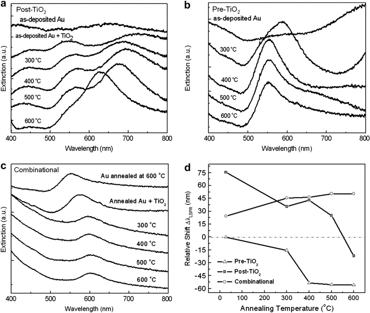
A set of extinction spectra for (a) the as-deposited and annealed Au/TiO2 core/shell nanoprism arrays (Post-TiO2); (b) the as-deposited and annealed Au nanoprism arrays (Pre-TiO2); (c) the as-deposited and annealed Au/TiO2 core/shell nanoprism arrays, with Au cores preannealed at 600 °C before the deposition of TiO2 (Combinational). The spectra were shifted vertically for clarity; (d) relative shifts of peak position of the in-plane dipole resonance as a function of the annealing temperature for the above three groups of experiments.
As a comparison, the same annealing processes were carried out for the bare Au nanoprism arrays, and the changes of the LSPR were measured (Fig. 5b, “Pre-TiO2”). The broad and weak LSPR band of the as-deposited Au nanoprisms became narrow and intense when the particles were annealed at 300 °C. Identified as the in-plane dipole resonance, the band made a blueshift with continuous increase of the intensity and narrowing of bandwidth. The decrease of bandwidth and increase of intensity after annealing were due to the reductions in morphological aberrations of the Au nanoparticles. The blueshift was caused by the transformation of the Au nanoprisms into nanospheres. Further annealing of the sample at higher temperatures (500 or 600 °C) induced no obvious change in the LSPR band, due to the completion of the transformation after annealing at 400 °C. The annealing-induced shape transformation was confirmed by an AFM study. 69
We aimed to recognize the effects of TiO2 on the LSPR of core/shell nanoprism arrays during the annealing. As such, we repeated the annealing processes on the Au/TiO2 core/shell nanoparticles, while preannealing the Au nanoparticles at 600 °C before depositing the TiO2 shells. The preannealing transformed the Au nanoprism into nanospheres, preventing the LSPR of the core/shell nanoparticles from being affected by shape changes. As a result, a single in-plane dipole resonance was observed before and after formation of the TiO2 shells (Fig. 5c). The shells induced a redshift of the resonance frequency. The thermal annealing caused the LSPR band to redshift continuously because of the increased refractive index of the TiO2 shells. This increase was caused by the crystallization under thermal annealing, as revealed by X-ray diffraction analyses of the TiO2 thin films (not shown).
To have a better idea of the thermal behavior of nanoparticles, Figure 5d gives the relative peak shifts of the in-plane dipole resonance as a function of annealing temperature for the three groups of samples: “Pre-TiO2,” “Post-TiO2,” and “Combinational.” The surface plasmons of the core/shell nanoprism arrays could be engineered by changing the shapes of the cores and the optical properties of the shells. The combinational effects enhanced the structures' surface plasmons, with their characteristics (e.g., resonance frequency, intensity, and bandwidth) meeting the requirements of different applications.
Au Nanodisk Arrays
We aimed to demonstrate the tailorability of our Au nanodisk arrays (Fig. 2). To achieve this, we systematically investigated how the disks' LSPR was affected by their geometric parameters (e.g., disk diameter and disk thickness) and their surroundings (e.g., Cr interfacial layers, substrates, and embedding fluids). The investigation provides a reference for future nanoengineering of surface plasmons by modifying one or more of the parameters of the Au nanodisks.
Figure 6a shows the experimental peak position and full width at half maximum (FWHM) of the LSPR band of asfabricated Au nanodisk arrays as a function of disk diameter. The inset in Figure 6a is a schematic of nanodisks with the same thicknesses and different diameters. When the diameters of the Au nanodisks were increased, the disks' LSPR peak redshifted and increased in intensity, while the FWHM broadened. The dependence of LSPR on disk diameter matched with that obtained in DDA calculations, except that the experimental data exhibited a much larger FWHM. The difference between the experimental and computational FWHM arose primarily from imperfect experimental conditions, such as defects, nonuniform disk sizes, and shapes. It has been found that thermal treatment of the nanodisk arrays could significantly narrow the FWHM by reducing the defects and unifying the morphology among the disks. 70
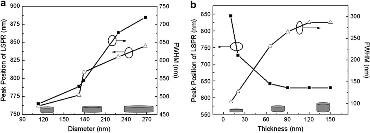
(a) Evolution of measured peak position and full width at half maximum (FWHM) of the localized surface plasmon resonance (LSPR) band of Au nanodisks as a function of the disk diameter. The inset is a schematic of the nanodisks of the same thicknesses and different diameters; (b) evolution of calculated peak position and FWHM of the LSPR band of Au nanodisks as a function of disk thickness. The inset is a schematic of nanodisks of the same diameters and different thicknesses.
The effects of Au nanodisk thickness on the LSPR were examined with DDA calculations. Figure 6b depicts the peak position and FWHM of the LSPR band as a function of disk thickness. The inset in Figure 6b is a schematic of nanodisks with the same diameters and different thicknesses. A decrease in the thickness of the Au nanodisk caused the LSPR peak to redshift and increase in intensity while the FWHM narrowed. Further, effects of Cr interfacial layers and substrates on the LSPR of Au nanodisks were examined based on DDA calculations. The calculations revealed that the substrates caused a redshift of the LSPR peak position with decreased peak intensity. The presence of a Cr interfacial layer caused a blueshift of the peak position and significantly reduced the intensity of the LSPR while broadening the FWHM.
Finally, we measured the dependence of LSPR of the Au nanodisks on refractive index of the embedding fluids by integrating the nanodisk arrays with microfluidic channels. Figure 7a is a schematic of a plasmofluidic chip that we used. Figure 7b shows the extinction spectra recorded from annealed Au nanodisks with a diameter of roughly 140 nm when different fluids flowed through the channels. Besides air (n = 1), four other fluids with different refractive indices were used: water (n = 1.33), acetone (n = 1.36), isopropanol (n = 1.37), and optical oil (n = 1.63). The LSPR peak position made a redshift with a slight increase of peak intensity whenever a fluid of higher refractive index was introduced into the channels. The observed effects of the surroundings' refractive index on the LSPR match well with the DDA calculations.
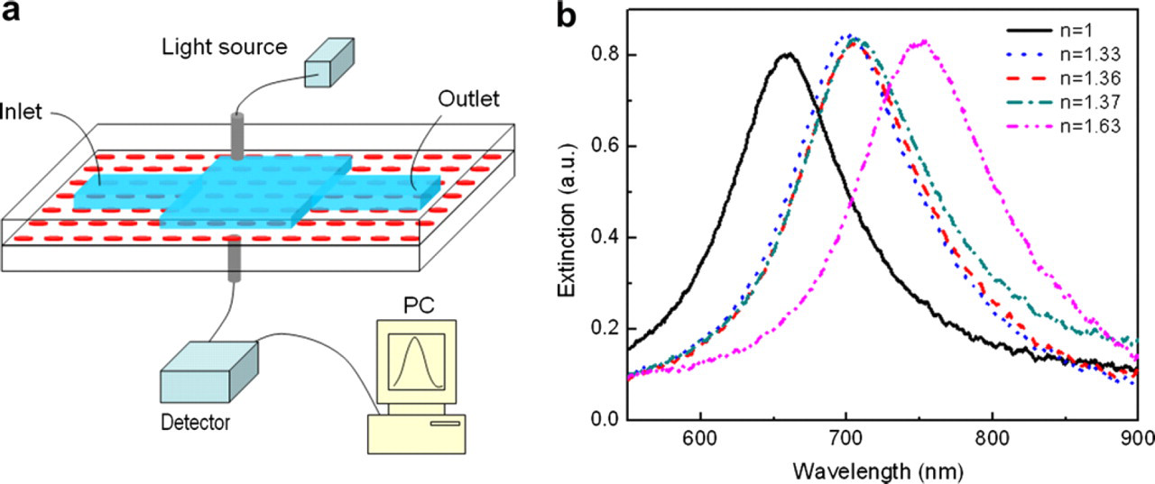
(a) Schematic of a Au nanodisk array-based plasmofluidic chip with an optical detection system; (b) extinction spectra of the Au nanodisk arrays as recorded from the plasmofluidic chip when different fluids flowed through the microfluidic channel.
Active Plasmonics
Our metal nanostructure arrays, combined with our nanoengineering methods for tuning the surface plasmon properties, will serve as a platform for both fundamental studies and practical applications in the field of plasmonics. The applications include nanophotonic devices, SERS, biological sensing and imaging, and “lab-on-a-chip” systems. 19,27,63,71 As an example, we demonstrated all-optical plasmonic switches/modulators with nanodisk arrays, as well as photoresponsive liquid crystals (LCs). These demonstrations contribute to the emerging field of active plasmonics, a field that will allow VLSEPI. 7,8,72 -74
Figure 8 gives an overview of major routes for active plasmonics: active tuning of dielectric constant of surrounding media; 75 -77 active tuning of the size/shape of metal nanostructures; 78 charge/discharge of metal nanostructures; 65,66,79 active tuning of interparticle distance; 80,81 and spinplasmonics. 82 LCs have potential applications in active plasmonic devices due to their birefringence, a large change in refractive index obtained by changing the alignment of the LC molecules. The concept has been demonstrated by several research groups, which achieved active tuning of the properties of surface plasmons (e.g., resonance frequency, bandwidth, resonance intensity, and the dispersion relation) of different plasmonic nanostructures embedded in LCs. The tuning in plasmonic properties was achieved by electrically or thermally controlling the alignment of the LCs. 83 -89 Compared with electric and thermal input signals, optical input has several advantages such as fast response speed and simultaneous monitoring of the tuned signals. 90
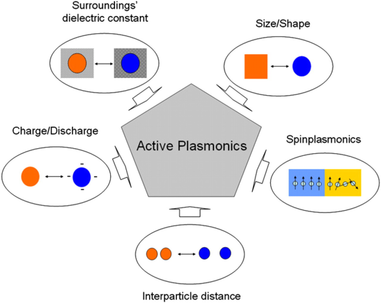
An overview of major routes for the development of active plasmonics.
To create photoresponsive LCs, we doped the LCs with a small amount of azobenzenes as photoswitchable guest molecules. As shown in Figure 9a, a nematic-isotropic (N-I) phase transition of the LCs was induced by trans-cis photoisomerization of azobenzene moieties dispersed in the LCs. Because the trans-cis photoisomerization in the azobenzenes was reversible, the N-I phase transition of the doped LC system could be reversibly tuned by controlling the photoirradiation with a pump light of suitable wavelength and power. The phase transition changed the refractive index of the LCs, which changed the LSPR of the Au arrays because their LSPR was sensitive to changes in the surroundings' refractive index. This change in LSPR enabled development of the all-optical active plasmonic switches/modulators. Figure 9b shows the change in the LSPR of Au nanodisk arrays embedded in the photoresponsive LCs upon photoirradiation with a pump light (20 mW @ 420 nm). The extinction spectra were measured with the probe light normally incident upon the nanodisk arrays. When the pump light was turned on, the LSPR peak blueshifted 30 nm and decreased in intensity. The lower intensity arose from the decreased light scattering by the LCs, because they had an initial isotropic phase after thermal treatment and were better aligned upon photoirradiation. Repeatable active tuning of the LSPR was achieved by alternatively switching the pump light ON and OFF.
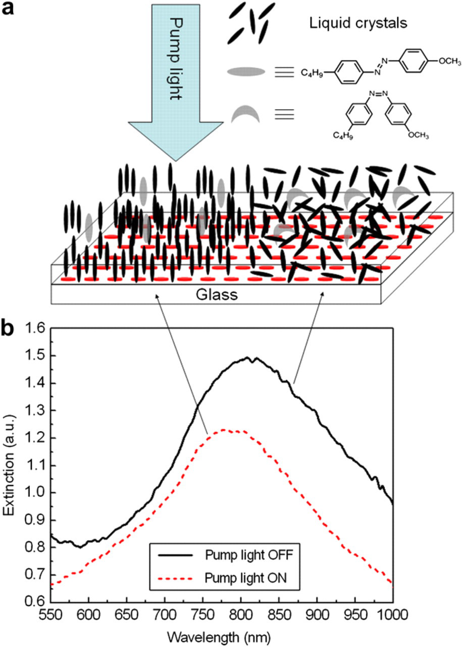
(a) Basic structure and working principle of all-optical plasmonic switches/modulators that were based on ordered Au nanodisk arrays and photoresponsive liquid crystals; (b) measured localized surface plasmon resonance spectra showing the peak shift and intensity change upon photoirradiation of the embedded nanodisk arrays by pump light.
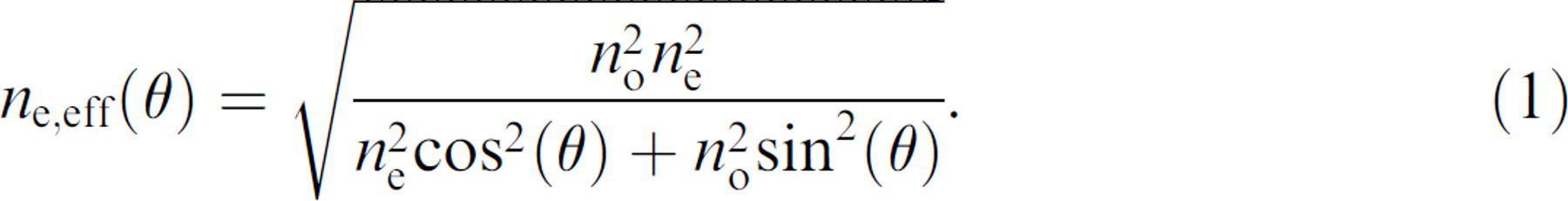
We aimed to understand the physical mechanism behind the peak shift of the LSPR of Au nanodisk arrays embedded in the photoresponsive LCs. To reveal the underlying mechanism, we quantitatively addressed the birefringence of LCs. Figure 10a shows the refractive index ellipsoid of a uniformly aligned LC system. The aligned system was treated as a single crystal. The single crystal had a refractive index determined by the polarization and propagation of incident light. There are two types of refractive index, extraordinary refractive index (n e) and ordinary refractive index (n o). These types corresponded, respectively, to the polarization of incident light parallel and perpendicular to the director axis (the z-axis in Fig. 10a). When the incident light impinged on the single crystal at an angle (θ) that was oblique with respect to the director axis, there was an effective extraordinary refractive index (n e,eff) given by Eq. (1):
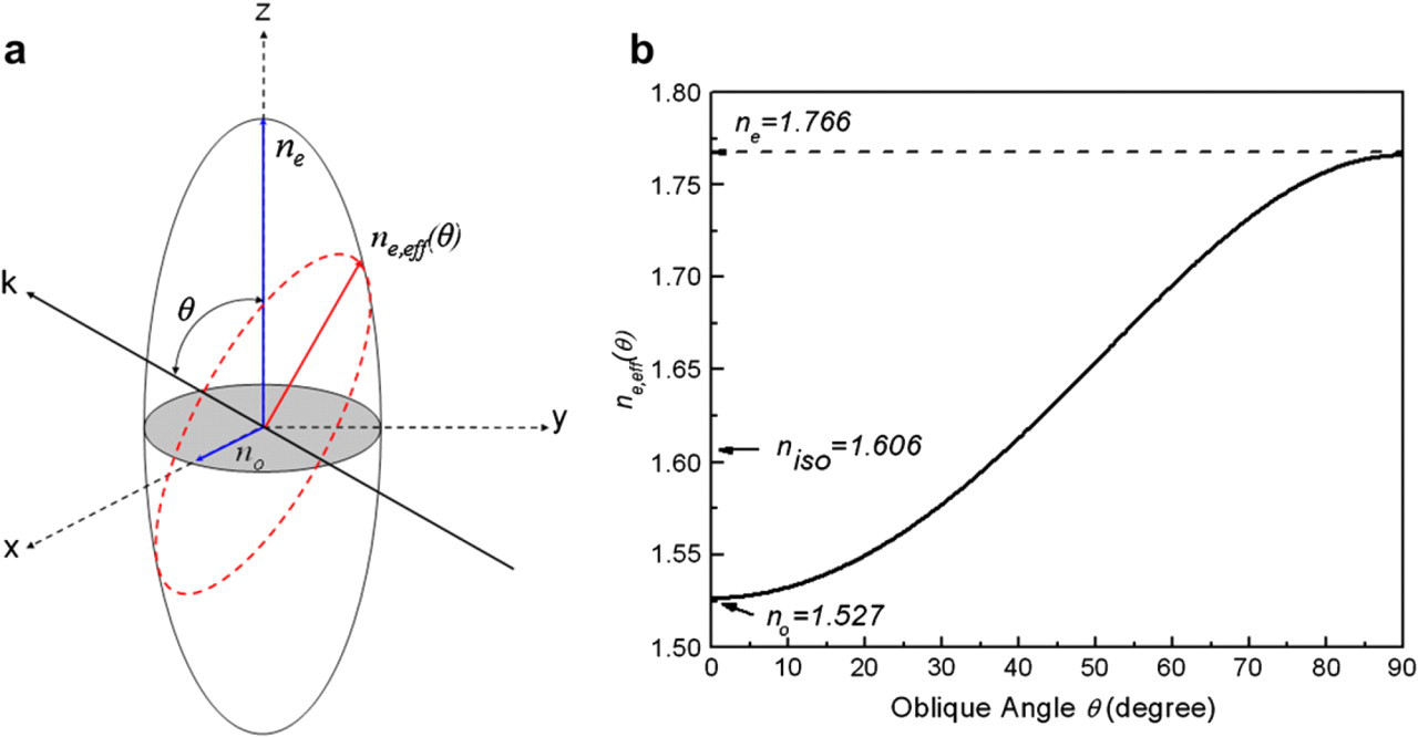
(a) Ellipsoid expressing the refractive index of a uniformly aligned liquid crystal (LC) system; (b) effective extraordinary refractive index of LCs as a function of oblique angle. For TL213 LCs, the extraordinary refractive index (n e) and ordinary refractive index (n o) of the nematic phase were 1.766 and 1.527, respectively, and the refractive index (n iso) of the isotropic phase was calculated as 1.606.
The θ-dependent n e,eff for the TL213 LCs is shown in Figure 10b. The single crystal had n e and n o of 1.766 and 1.527, respectively. The n e,eff increased continually from 1.527 to 1.766 over θ from 0° to 90°. For isotropic LCs of random alignment, the refractive index was independent of the propagation and polarization of incident light, and was calculated according to Eq. (2):

For the TL213 LCs, n iso was calculated as 1.606.
To model the experimental situation, we assumed that the Au nanodisk arrays embedded in the LCs were in the x-y plane and the probe light propagated along the z-axis. In this case, the probe light encountered a refractive index of 1.606 (n iso) when the LCs exhibited an isotropic phase with the pump light OFF. On photoirradiation, the LCs transited from an isotropic to a nematic phase. The blueshift in the LSPR meant a reduced refractive index of the LCs experienced by the probe light, indicating that the nematic LC single crystal was aligned with the director axis along the normal to the substrate (Fig. 9a). However, the quantitative analysis of the LC alignment can be challenging due to the presence of Au nanodisks on the substrate. To better model the exact information on the LC alignment before and after photoirradiation, one would need to do extra spectroscopic studies such as incident angle- and polarization-dependent measurements of LSPR, or three-dimensional imaging of the LCs. Additionally, for a more accurate analysis of functionality of the plasmonic hybrid nanostructures, one should consider how doping affects the refractive index of LCs.
Conclusion
Plasmonics is an emerging field that will yield novel photonic and medical nanodevices of great benefit to humanity. Although much progress has recently been made in the field, there are still many challenges in the fundamental understanding and devising applications of plasmonic phenomena. The first and one of the most significant challenges is nanofabrication, especially the low-cost and high-throughput production of metal nanostructures with tailorable plasmonic properties. We addressed this challenge by developing cost-effective and high-efficient fabrication techniques and effective nanoengineering approaches for metal nanostructure arrays of various shapes and sizes. We quantitatively analyzed the effects of engineered parameters (e.g., shape, size, and surroundings) on the LSPR of the metal nanostructure arrays. Our findings qualify these metal nanostructure arrays as a platform for fundamental plasmonic research and as core nanostructures in plasmonic devices and systems. As an application of the arrays, we developed an active plasmonic hybrid nanostructure that was based on an ordered Au nanodisk array embedded in photoresponsive LCs. The all-optical active nanostructure resulting from our work can be used in high-density optical storage media, optical filters, and switches, and contributes to the development of integrated nanophotonic circuits.
Acknowledgments
This work was supported by Air Force Office of Scientific Research, the NSF NIRT grant (ECCS-0609128), and the Founder's Prize and Grant of the American Academy of Mechanics (sponsored by Robert M. and Mary Haythornthwaite Foundation). Components of this work were conducted at the Penn State node of the NSF-funded National Nanotechnology Infrastructure Network. The authors thank Thomas R. Walker for helpful discussion.