Abstract
Here, we present an approach to design, fabricate, and create a simple, low-cost, and rapid prototyping crossbar junction using a p-type and n-type multiwalled carbon nanotubes (MWCNTs) via microcontact printing. This is achieved using poly-dimethylsiloxane (PDMS) molds. The parallel relief structure in order of a few micrometers is used to transfer continuous horizontal arrays of these MWCNTs in aqueous suspension. Using an alignment and the stamping process, PDMS molds are inked alternatively with p-type and n-type MWCNTs suspensions and transferred in a grid-like manner onto the base microelectrode platform. Parallel alignment of these MWCNTs is achieved due to the geometry of the mold relief structures. The hierarchical assembly results in the formation of the crossbar array structures. The functionality of this circuit has been demonstrated through the current–voltage (I–V) characteristics associated with the junction formation.
Keywords
Introduction
Over the past few years, formation of functional assemblies using multiwalled carbon nanotube (MWCNT) nanostructures has become a prime focus of research in the field of nanotechnology, with focus on the symmetrical alignment and the patterning of nanomaterials for integrated nanosystems. Fabrication of these complex high-density integrated nanodevices using nanoscale materials is a demanding and challenging exploration in the nanoelectronic world. MWCNTs, which are on the order of a few tens of nanometer show novel properties in terms of stiffness, toughness, and improved conductivity. Nanodevices fabricated from these MWCNTs show improved efficiency and performance due to the increased surface area to volume offered by these nanostructures.1, 2 In spite of these various advantages, repetitive, symmetric patterning, and alignment in terms of positioning, fabricating, and assembling them into nanodevices always has been a challenge.3–6
Numerous methods have been demonstrated for constructing crossed nanomaterial junctions. Atomic force microscope (AFM) 7 has been used in positioning the nanomaterials, modulating nanomaterials with chemical doping, and for adsorbing nanomaterials with organic molecules.8, 9 Recently, a wide variety of alignment techniques, such as Langmuir Blodgett method10, 11 and the superlattice nanowire pattern transfer method, 12 have been used for the fluidic alignment and surface patterning of nanomaterials based on their inherent or modified hydrophilicity to form arrays of nanodevices. The above methods have disadvantages of limited control over spacing between two nanostructures. Furthermore, these methods, despite producing arrayed nanostructures, are highly complex and difficult to implement. All these techniques either have low probabilities of success due to their highly selective manner of nanomaterial deposition or require vacuum conditions, greatly limiting their mass production for practical applications.
In contrast, we have developed a high-density crossbar array junction prototype using a simple, rapid, and low-cost microcontact printing technique that has the capability of being automated. Integrating this soft lithography technique for relief imprinting and the standard photolithography technique for fabrication of microelectrode platform, multiple crossbar junction device prototypes were developed. The functional devices were built using MWCNTs, which were patterned using coated carbon nanotubes poly-dimethylsiloxane (PDMS) molds coated with MWCNTs to print onto the base silicon substrate having array of metallic gold micron size electrode fingers.
The crossbar nanoarrays have a wide range of potential applications in the form of various diode/Field Effect Transistor (FET)-based devices for bio/chemical sensing in the life sciences industry.13, 14 In these devices, the detection of the specific species occurs due to the modulation of charge transport in the junctions. These devices can function as Ion Selective Field Effect Transistors, where biochemical species produce ionic modulation in the FET characteristics.15–17 In our research, we anticipate that the electrical parameters associated with the crossbar nanoarray device (voltage and current) will be modulated when it functions as a bio/chemical sensor Crossbar nanojunction serve as potential receptor sites for detecting species from ambient media such as air and water. Thus, these devices have promising applications for identifying biomolecules such as proteins and viruses. The species attaching or adsorbing on to the crossbar junction will modulate the charge carrier transport at the junction and modify junction characteristics due to the surface charge associated with the charged species. We are currently focusing on demonstrating these devices functioning as a bio/chemical sensor.
Methods and Materials
The engineering of crossbar junction device involves the following three steps. (1) Fabrication of microelectrode platform for electrical characterization. (2) PDMS stamp fabrication for imprinting nanomaterial. (3) Pattering MWCNTs (Fisher scientific, USA) for nanojunction formation.
Fabrication of Microelectrode Platform
The microelectrode platform consists of gold metallic microelectrode array, which incorporates four microcontact fingers. The silicon-base platform design consists of two microfingers placed opposite to each other and the other two microfingers rotated by 90°. These base microcontacts on the silicon substrate are incorporated to acquire an electrical signal from the nanodomain. This microelectrode platform was fabricated using standard photolithography techniques. The process sequence follows spin-coating polymeric ultraviolet (UV) sensitive photoresist on the silicon on insulator, pattern transfer using UV light, pattern development using developer, depositing gold using sputtering method, and final step involves photo lift off using solvent. Figure 1 shows intermediate optical image of single microcontact finger during the fabrication process. The microcontact end-tip dimensional width is approximately 50 μm, placed 100 μm apart. An electrical connection to the external power supply and measuring devices is achieved by increasing the end-tip size of microcontact fingers in the graded step size to approximately 3 mm to have a large base-contact width. The I–V characteristic of crossbar-assembled nanostructures is measured using these microcontact fingers.
Optical images depicting the single microelectrode finger in a 2 × 2 array. (a) Developed polymer photoresist microelectrode finger pattern on the base Si substrate. (b) Uniform deposition of gold film using sputtering method. (c) Metallic gold electrode for electrical characterization.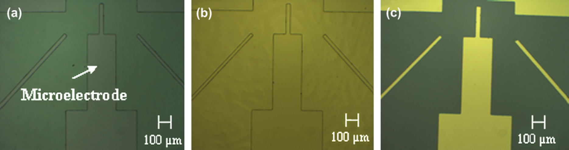
PDMS Stamp Fabrication
The nanomaterial is assembled and pattern transferred onto the fabricated silicon-base microelectrode platform using a polymer stamp having a relief structure of desired prototype. The PDMS stamp with positive relief structure serves as the stamp for transferring the MWCNTs and is achieved by first fabricating on silicon master mold having negative structure using standard photolithography techniques. The parallel relief structure of the stamp is developed with the negative microchannels on the master template created by photoresist. The master template has microchannels of varying width of approx. 50–250 μm. The gradations were used to empirically determine the dimension of the parallel structure that would achieve the optimal transfer of the nanomaterials between the microelectrodes. The soft and flexible polymeric stamp was created using PDMS. The process sequence consists of mixing elastomer and curing agent, degassing the air bubbles in vacuum chamber, which are formed during mixing and finally pouring the viscous elastomer liquid onto the master mold and curing on the hot plate. Due to the cross-linking of polymer, the polymer stamp does not disintegrate, can be easily peeled off, and separated from the master template. Figure 2 shows an optical micrograph of Si master mold in (a) and PDMS stamp in (b).
Optical image (a) Si master mold for creating elastomeric stamp (b) Poly-dimethylsiloxane stamp for nanomaterial imprinting.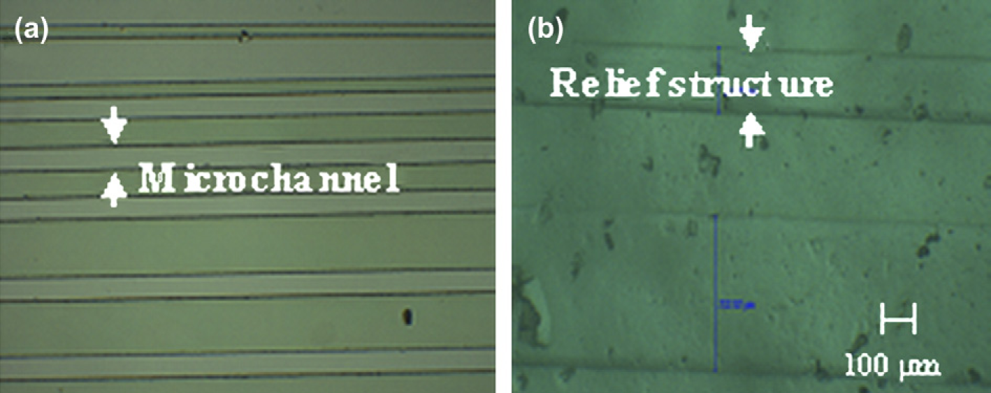
Patterning MWCNTs
The patterning technique incorporates parallel relief microcontact printing for aligning of nanoscale one-dimensional MWCNTs. The above polymeric stamp–having parallel horizontal relief structure is inked with MWCNTs by immersing the mold into MWCNT aqueous suspension. The thin film MWCNT aqueous suspension of approximately 20 mm is formed into petri dish of depth 1 cm. Later, MWCNT layer is transferred onto base substrate by applying gentle thumb pressure of about 1 N over an area of 1 cm2. To establish the parallel alignment of MWCNTs at the center of 1 × 1-cm2 clean silicon substrate, AFM characterization of the parallel stamping process was performed. Figure 3 demonstrates the accurate parallel pattern transfer of the p-type MWCNTs, which is the first step in the p–n junction formation. These horizontal parallel arrays of p-type MWCNTs are observed in AFM. The AFM figure confirms parallel impression of the p-type MWCNTs arrays by observing alternate light and dark bands representing presence and absence of MWCNTs, respectively. Although stamp-having arrays of perfect continuous horizontal relief structures were used for p-type MWCNT pattern transfer, imperfect discontinuous horizontal pattern transfer is noticed as a result of Rayleigh instability. In addition, yellow droplets are also observed during characterization and can be correlated to higher topographical elevations that occur due to the clustering of MWCNTs. These MWCNT clusters at regular interval can be speculated as a result of Rayleigh capillary instability and not due to the formation of crossbar junction.
Atomic force microscope characterization of patterned p-type MWCNTs in parallel array via microcontact printing.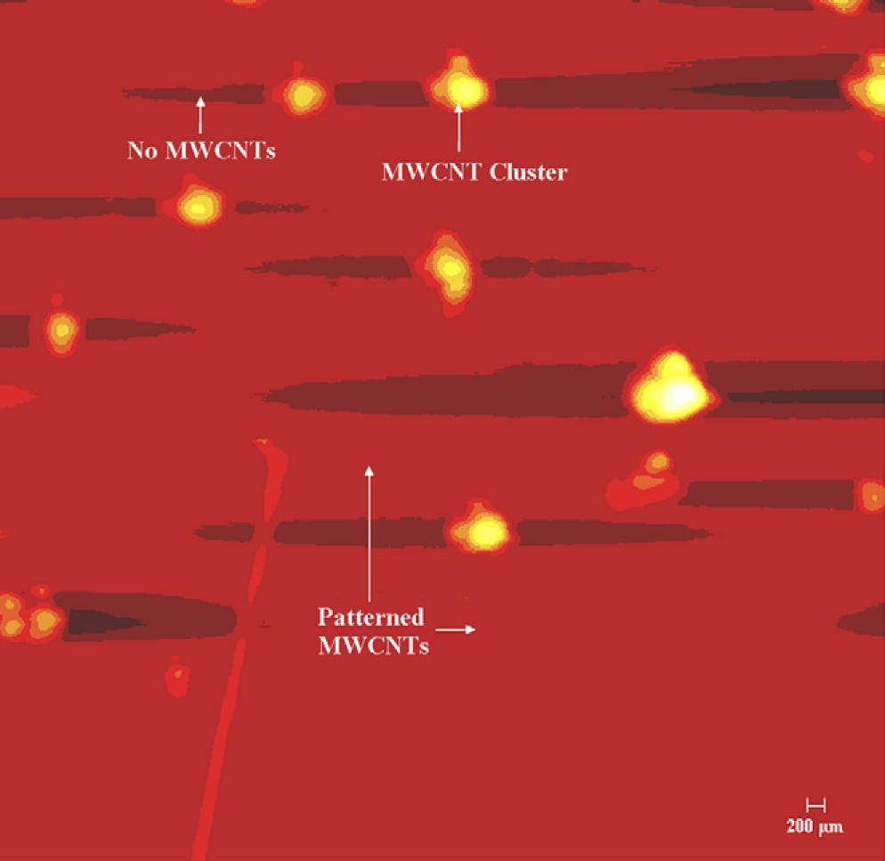
Now, the inked stamp is aligned to pattern n-type MWCNTs in crossed configuration onto the base microcontacts. Due to the cross-fashion relief microcontact printing, there is a formation of crossbar junction of aligned p-type and n-type MWCNTs at the interface. The conceptual formation of a crossbar junction is shown in Figure 4. The junction characteristic behavior is measured and observed by I–V characteristics.
Schematic diagram illustrating nanojunction formation using p-type and n-type MWCNTs patterned in crossbar fashion.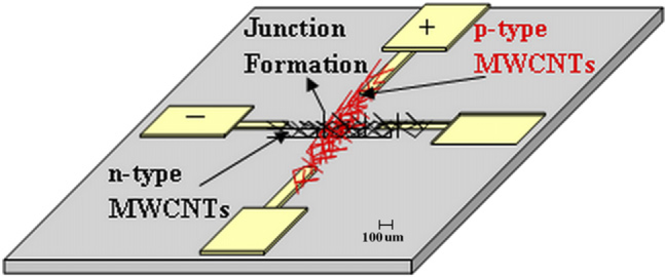
Results
Various unpatterned nanomaterials show resistive lump behavior with varying conductivity depending upon the material characteristics. It is also observed that randomly dispersed p-type and n-type MWCNTs show an Ohmic characteristic. When patterned and assembled, the characteristic behavior of the fabricated nanodevices changes drastically. I–V characteristics were measures for two different configurations. For unpatterned MWCNTs, the device shows resistive lump behavior while the crossbar nanojunction formed due to the pattern p-type and n-type MWCNTs shows forward junction behavior. Figure 5 shows the I–V characteristic of unpatterned p-type and n-type MWCNTs in (a) and patterned p–n junction MWCNTs in (b). This is due to the fact that there is an electron transport through multiple shells and electron tunneling between adjacent MWCNTs. Standard lead base address lines are used for probing these microelectrodes and used to measure rectifying junction behavior. The results indicate that the microcontact imprinting technique may prove useful for prototyping rapid and inexpensive nanoscale devices. In addition, this technique provides the capability of simultaneous patterning of both similar and disparate nanomaterials. Thus, it is a faster technique than the standard nanolithography techniques for nanodevice fabrication.
Current–voltage (I–V) characteristic graph (a) unpatterned MWCNTs showing resistive lumped behavior and (b) patterned MWCNTs showing forward junction behavior.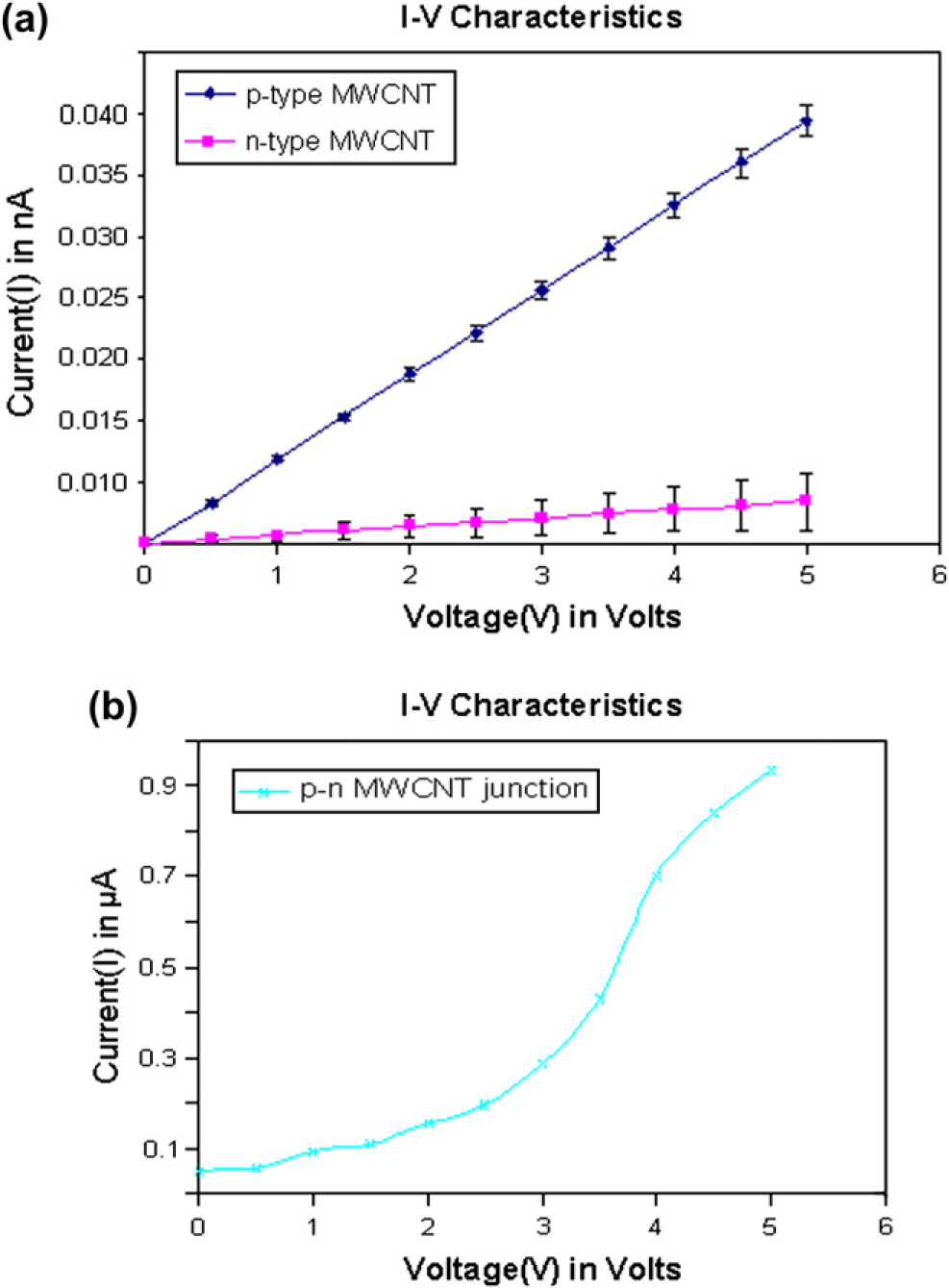
Conclusion
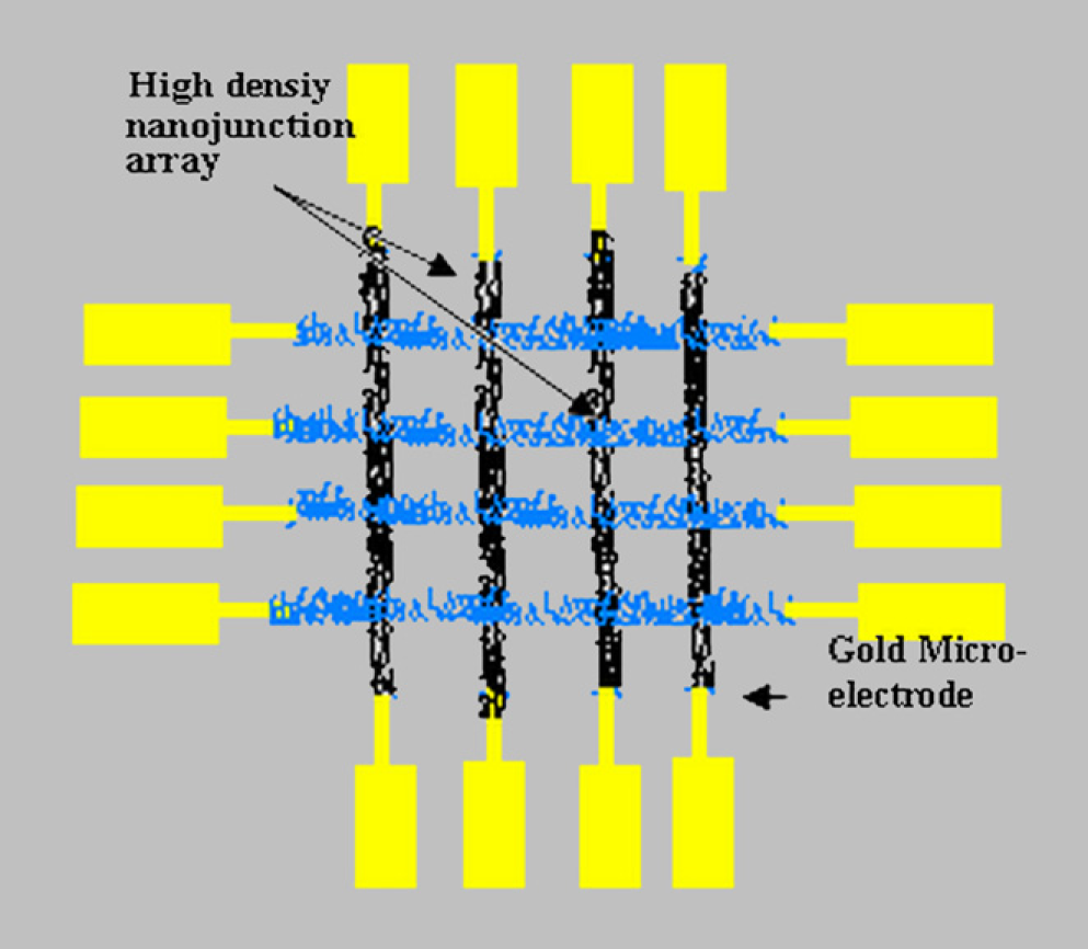
The need for automated high-density device constructed at the nanoscale has led to an investigation of various nanomaterials and techniques associated with assembling, patterning, and fabricating nanoscale devices. In this article, we have explored the relief microcontact printing technique for simultaneous and rapid assembly of MWCNTs to potentially supplant individual and slow assembly techniques such as electron beam lithography. The polymer PDMS stamp printing technique has advantages in terms of time and cost per structure. Figure 6 is the conceptual drawing of a high-array density nanojunction that can be fabricated using microcontact printing. In brief, we have explored a cost-efficient fabrication method for MWCNT crossbar nanojunction arrays that uses simple, rapid, and low-cost microcontact printing. The I–V characteristics show a junction behavior characteristic comparable to those formed using complex, clean room, and high-cost nanofabrication techniques. The crossbar junction shows promising results that could lead to development of p–n junction diodes, which in turn can be used as a bio/chemical sensor for life science applications. The long-term goal would be to form the high-density cross-array circuit patterns to develop an array of “devices” with an array of gold electrodes, fabricated on the silicon substrate. Using these high-density cross-array circuit patterns, the nanosensor, geared toward the development of complex devices, could form the building blocks of highly multiplexed sensor platform.
Schematic diagram demonstrating the high-density crossbar junction array formation using relief imprinting technique.