
Abstract
We demonstrate a technique to detect protein biomarkers contained in vulnerable coronary plaque using a platform-based microelectrode array (MEA). The detection scheme is based on the property of high specificity binding between antibody and antigen similar to most immunoassay techniques. Rapid clinical diagnosis can be achieved by detecting the amount of protein in blood by analyzing the protein's electrical signature. Polystyrene beads which act as transportation agents for the immobile proteins (antigen) are electrically aligned by application of homogenous electric fields. The principle of electrophoresis is used to produce calculated electrokinetic movement among the anti-C-reactive protein (CRP), or in other words antibody funtionalized polystyrene beads. The electrophoretic movement of antibody-functionalized polystyrene beads results in the formation of “Microbridges” between the two electrodes of interest which aid in the amplification of the antigen—antibody binding event. Sensitive electrical equipment is used for capturing the amplified signal from the “Microbridge” which essentially behaves as a conducting path between the two electrodes. The technique circumvents the disadvantages of conventional protein detection methods by being rapid, noninvasive, label-free, repeatable, and inexpensive. The same principle of detection can be applied for any receptor—ligand-based system because the technique is based only on the volume of the analyte of interest. Detection of the inflammatory coronary disease biomarker CRP is achieved at concentration levels spanning over the lower microgram/milliliter to higher order nanogram/milliliter ranges.
Keywords
Introduction
Most quantitative immunoassays use fluorescence/luminescence detection schemes which display the quantity of analyte present in the sample proportional to the intensity of light emitted. 1 Current commercially available immunoassay-type detection techniques involve high-throughput detection of the analyte using the corresponding enzyme-labeled antibody. Ongoing research on drug delivery and immunoassay-based analysis systems strive to increase throughput and overall efficiency in clinical diagnostic applications. Analogous to incorporating a fluorescent tag to a bioreceptor molecule for fluorescent detection techniques, surface chemistries of synthetic polymer beads can be modified appropriately with the desired receptors to produce equivalent conclusions using optical and electrochemical detection techniques. 2 , 3 The latter, however, will not require expensive imaging equipment for capturing electrical signals arising from the chemical reactions between the biological agents. As electrical measurement systems combine acquisition and analysis of their electrochemical counterparts, they are more economical than optical measurement systems. Beads are not only readily available and offer a wide range of sizes but also provide a large surface area for functionalization unlike flat surfaces. Hence, polystyrene beads were used as the platform for immobilizing protein molecules to aid in the electrical detection of the biomolecule of interest.
Here, we report an electrical detection mechanism, which identifies electronic signals emanating from the antigen–antibody binding action occurring on the surface of the chemically modified beads. Analysis of the electrical data acquired from the formation of the antigen–antibody binding complex determines the presence of the protein of interest. Latex microspheres/polystyrene beads have been used as robust carriers for the proteins to facilitate better control of the nanoscale analyte. A well established electrokinetic mechanism, electrophoresis, is used to create homogenous fields in the fluid medium containing polystyrene beads. 3 This method helps in interrogating the colloidal particles suspended on the surface of the protein sensor chip to form electrical assemblies of bridge like structures. Sensitive electrical measurement devices tap into the biological reaction processes and acquire the electrical data necessary to validate the identification of the analyte.
Measurement Methods and Materials
Modeling of Base Microelectrode Array (MEA)
The planar MEA consisted of four microelectrodes. The design of the size and geometry of the microelectrodes is accomplished by using COMSOL Multiphysics (The COM-SOL Group, Stockholm, Sweden). Equivalent modeling of electromagnetic field effects inside and around the microelectrodes was studied and the MEA was fabricated by means of photolithography based on the conclusions of the simulation models. Figure 1 clearly displays the effects of the electric fields on the microspheres in fluid medium. The corners of the staircase-like regions of the electrode experience higher electric field intensities and thus attract a larger volume of beads. The scale of electric field intensity ranging from 0 V/m (represented in blue) to 3E 4 V/m (represented in red) is depicted at the bottom of the simulated electrode design. The optical image of the actual protein sensor chip and the simulation are in perfect agreement with respect to the alignment of beads. Effects of phenomena such as heat transfer and fluidic flow were analyzed, results of which were incorporated into the electrode design. Particle tracing was also put into effect to study the nature of the forces experienced by the polystyrene beads while in fluid.
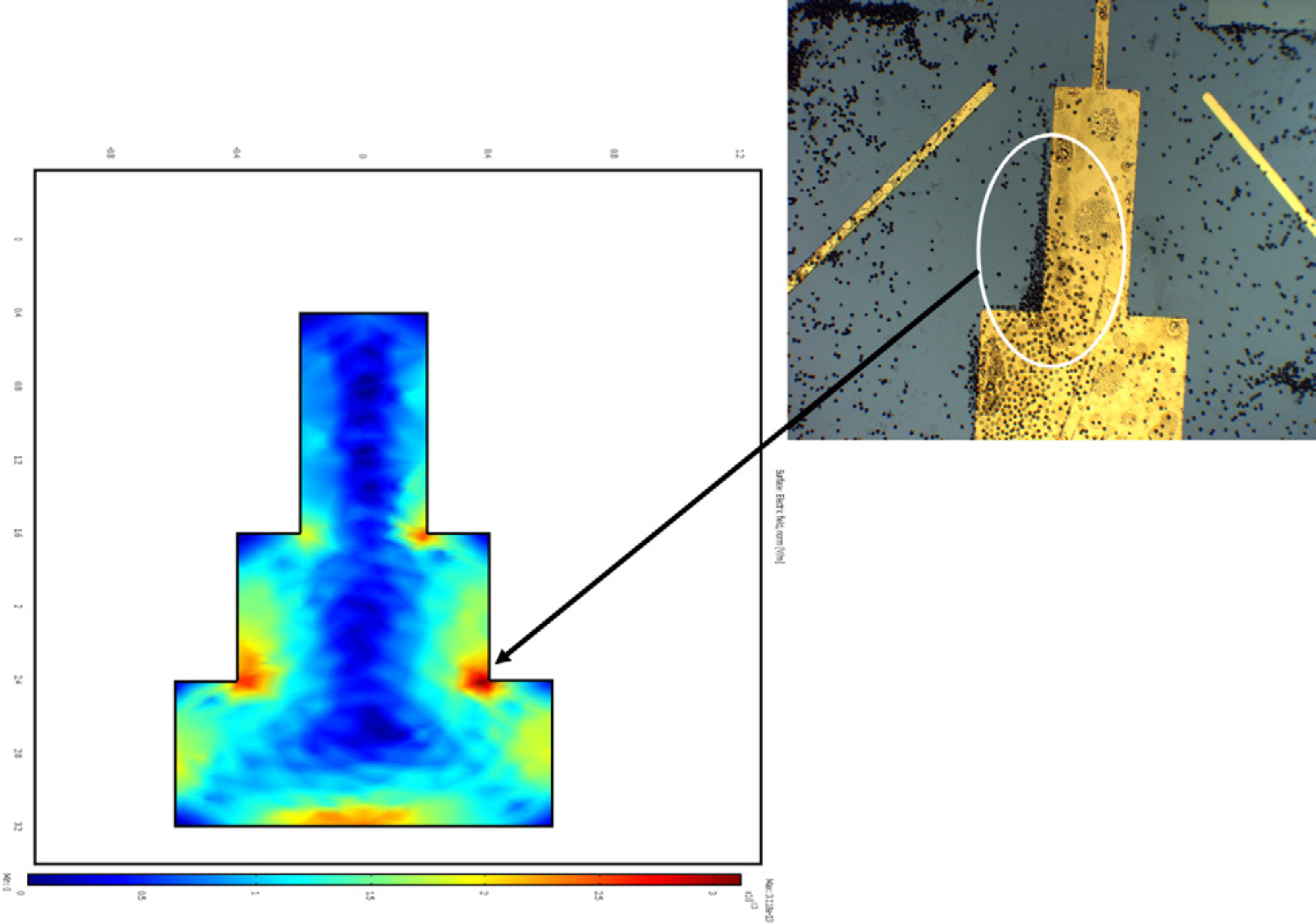
Comparison of software simulated electrode model and the actual electrode with the applied direct fields. The polystyrene beads are seen to accumulate at the corners of the step-like electrode where the strength of the electric fields are highest.
Microfabrication of Base MEA
Standard photolithography methods were used to fabricate the MEA. 4 Silicon substrate consisting of 1 mm thick phosphorous doped SiO2 is used as the platform for the MEA design. The substrate is first cleaned with piranha solution–a mixture of sulfuric acid and hydrogen peroxide in the ratio of 8:3 at 90 °C for about 30 min. Deionized water (DI water) was then used to wash the surface for 1 min after which the cleaned substrate was air-dried using dry nitrogen (N2) gas. Positive photoresist–Shipley 1827 (MicroChem, Newton, MA, USA) was spin-coated on the cleaned surface at 4000 rpm for 30 s to obtain a thickness of 3 mm. The resist coated substrate was then soft baked at 115 °C for 5 s. Contact lithography was carried out using a mask containing the electrode pattern and the photoresist-coated substrate and then exposed to UV light at 365 nm for 7 min wherein the initial 5 min was necessary for the UV lamp to attain its peak intensity. The mask-exposed substrate was then allowed to develop in a solution of Micro Dev Developer and DI water in a ratio of 1:1 for 80 s. The developed substrate was then carefully dried in N2 gas. This sample is observed under a microscope for checking the consistency of the pattern transfer. Chromium was evaporated using an electron beam evaporator to form a uniform layer of 100-nm thickness on the silicon dioxide surface. Gold is then evaporated to form a fine film of 10-nm thickness on the chromium layer. The double layer of chromium and gold is used to overcome the disadvantage of the poor adhesion of gold to silicon dioxide. Gold is then sputtered on the MEA pattern for 2 min to obtain a metal thickness of 120 nm ensuring a non-nucleated uniform coating. Standard acetone lift-off method was used to remove unwanted material on the substrate after which the sample is rinsed in DI water and dried in N2 gas. This results in the desired MEA pattern which can be used for further experimentation. Figure 2 pictorially explains the process flow for fabrication of the base MEA.
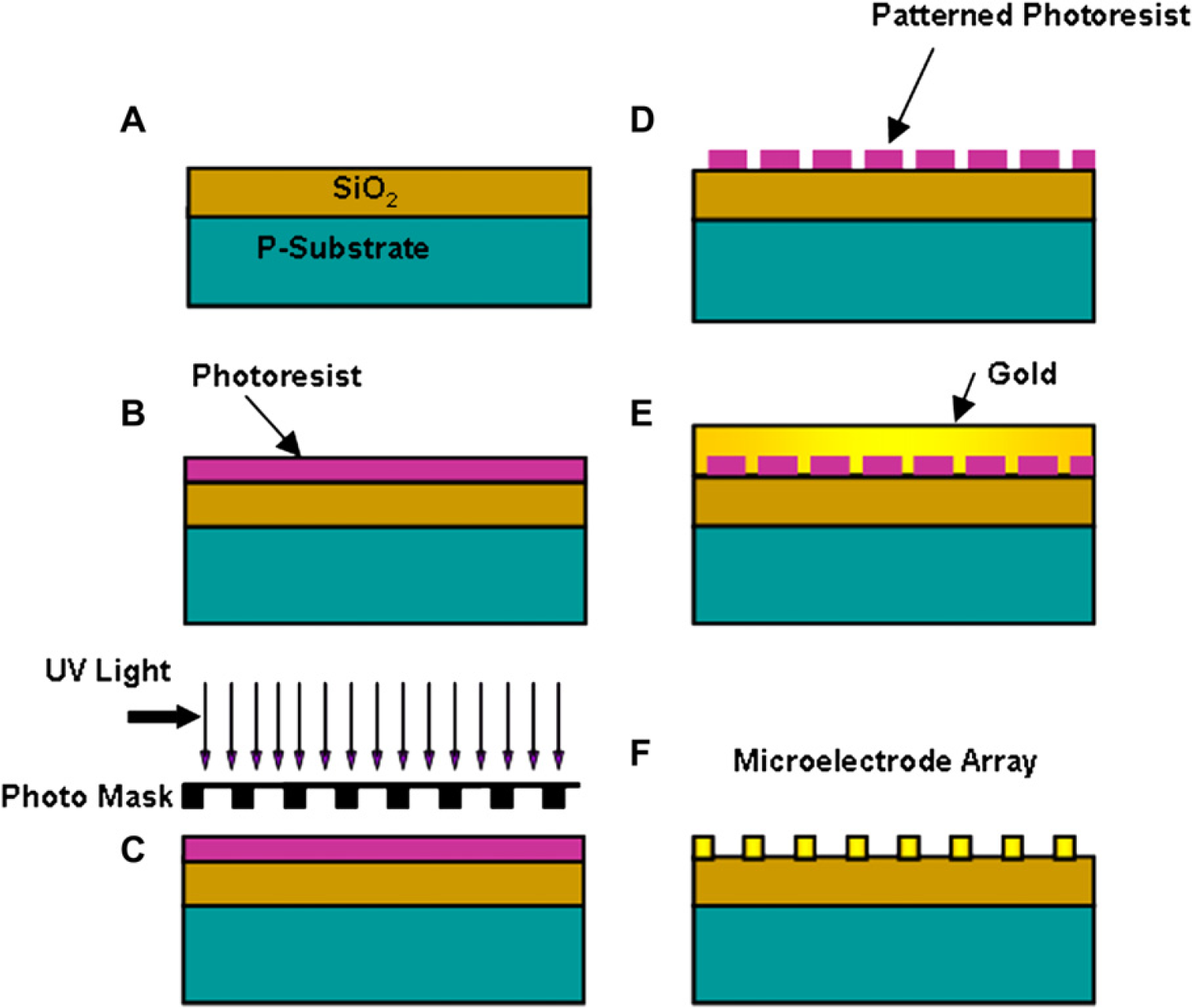
Process flow for micro-electrode fabrication using standard photolithography. (A) Cobalt doped silica-on-silicon substrate. (B) 3 μm thick positive photo resist spin coated OH 3500 rpm. (C) Spin coated photo resist soft baked at 115°C. (D) The soft baked photo resist is exposed to UV light with power densities on the order to 6.5 m W/cm 2 for 390 seconds at 365 nm. (E) The exposed photo resist pattern is developed in a solution micro posit developer arid D. 1. Water in 1: 1 ration by volume and dried with dry NZ. (F) Gold is sputter coated onto the developed substrate.
Experimental Setup
Initial electrical measurements are acquired and analyzed using the photolithographically fabricated MEA to validate the correct working of the biochip. Micromanipulators are used to establish contact between the measuring system and the contact pads on the MEA. A silicone chamber is used to enclose the functionalized polystyrene beads on the MEA and provide a static volume of solution necessary for conducting the experiment. A gradient homogenous electric field is applied to two of the microelectrodes of the MEA between which the “Microbridge” is desired to be formed. The electrophoretic movement of the antibody-functionalized polystyrene beads on the microelectrode surface is captured by the microscope fixed above the experimental setup. Figure 3 is a schematic representation of the entire experimental setup as achieved in the laboratory.
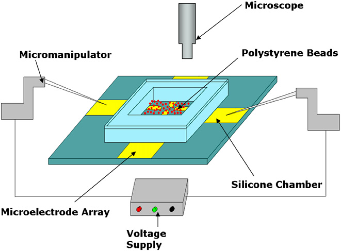
Schematic representation of the experimental set-up.
Construction of Flow Cell
After determining the correct working of the microelectrode sensor platform resulting from photolithography as described above, it is incorporated into a polydimethylsilixane (PDMS) encasement engineered to support the base chip for further interrogation during the protein-detection process. Figure 4 is a schematic representation of the flow cell device and Hamilton syringes containing the experimental fluids. (A) The Hamilton syringe containing the antibody-functionalized polystyrene beads is first injected to fill the silicone chamber on the surface of the chip followed by the injection of the analyte solution after the formation of the “Microbridge.” Figure 4 (B) explains the function of the flow cell device. The polymeric package comprises a total of three polymer microtubules (diameter of lumen 100 mm) positioned at precalculated sites during the curing of the polymeric enclosure. The microtubules are fitted with luer-lock needle holders to enable the use of calibrated syringes for administering the various experimental fluids on the sensing area of the sensor chip. Two of the microtubules are positioned such that their tips open directly over the sensing site of the chip. One of these two microtubules above the sensor platform is used for dispensing the antibody-functionalized polystyrene beads, whereas the other is used for dropping the analyte on the surface after the electrokinetic formation of the “Microbridge.” The third microtubule is placed such that its tip contacts the surface of the chip and is capable of draining the analyte mixture after one experimental iteration. The diameter size and the length of the microtubules are chosen to deliver calculated amounts of the experimental fluids at specific sensing sites on the biochip's surface. Figure 5 shows the optical micrographs of the above described flow cell device.
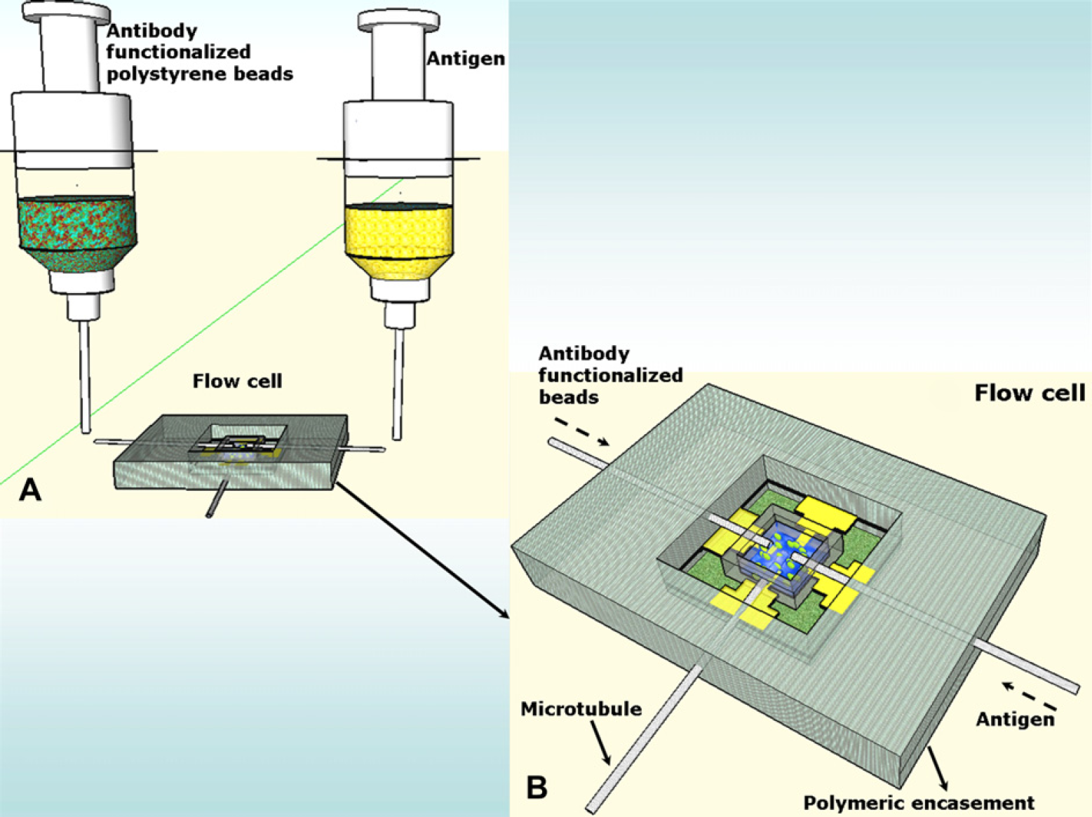
Schematic representation of the Flow Cell System. (A) Hamilton syringes containing the experimental fluids to be introduced into the flow cell. (B) Schematic of the flow cell device.
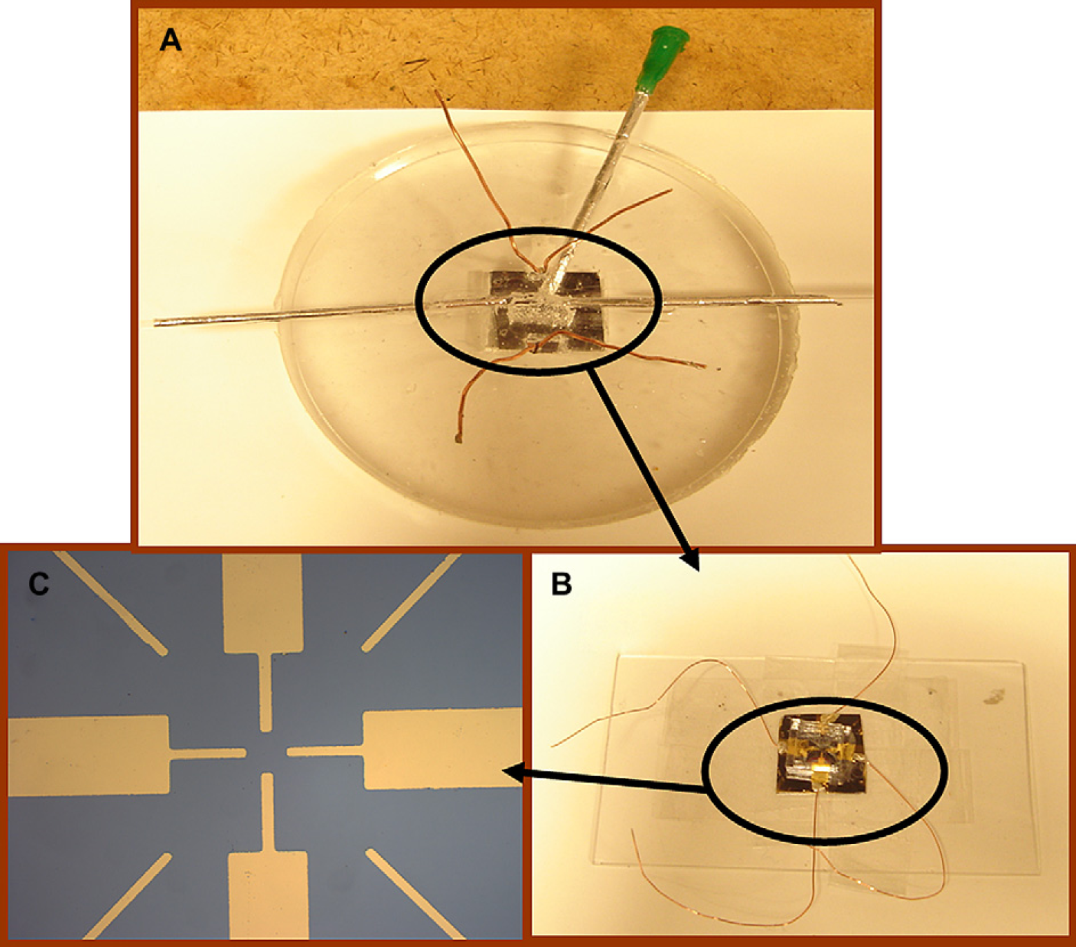
Flow cell device. (A) An optical micrograph of the Lab on a Chip device used for the formation of the “Microbridges.” The device comprises of a base MEA encapsulated by a polymeric package and (B, C) represents the core of the device and base platform.
Measurement Method
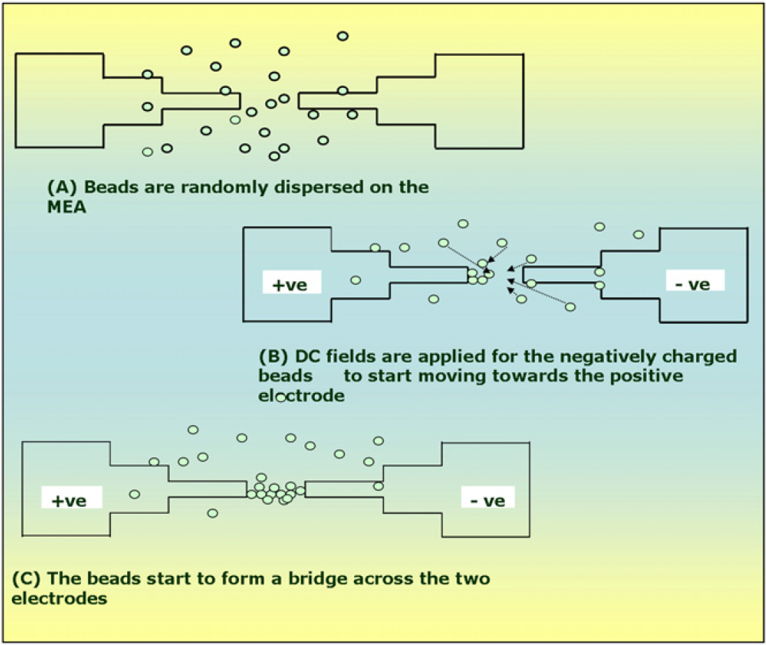
Control measurements are first acquired from the base platform from the bridge structure before the introduction of analyte solution. The antibody coating on the polystyrene beads imparts a surface charge on the polystyrene beads which is used for electrical arraying of the beads to form meaningful structures across the MEA. Figure 6 shows the formation of the “Microbridge” structure of the anti-C-reactive protein (CRP)-functionalized polystyrene beads when electrically aligned to form a conductive path between two electrodes by the application of homogenous fields across them. 4 The electrical signal measurements from the anti-CRP-functionalized polystyrene beads are tabulated. A calculated volume of antigen (CRP) is then dropped on this “Microbridge” structure to enable the binding reaction between the antigen and antibody on the surface of the polystyrene beads. The positioning of the beads in the bridge structure is such that the electrical signals arising from the antibody–antigen binding event get amplified due to the coupling effects between the various beads involved in the structure of the “Microbridge.” The amplified signal is acquired using sensitive measuring equipments such as the Keithley nanovoltmeter (Keithley Instruments Inc, Ohio). Signal acquiring and processing software LABVIEW (National Instruments, Austin, Texas) is incorporated into the measurement system to acquire real-time signals from the chip. Signals are measured dynamically by continuous recording of the electrical variations over time and analyzed to give quantitative results.
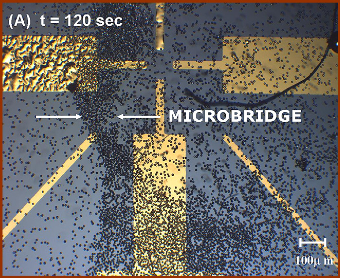
Antibody functionalized polystyrene beads form a “Microbridge” across the selected electrodes.
Discussion and Results
Principle of Operation
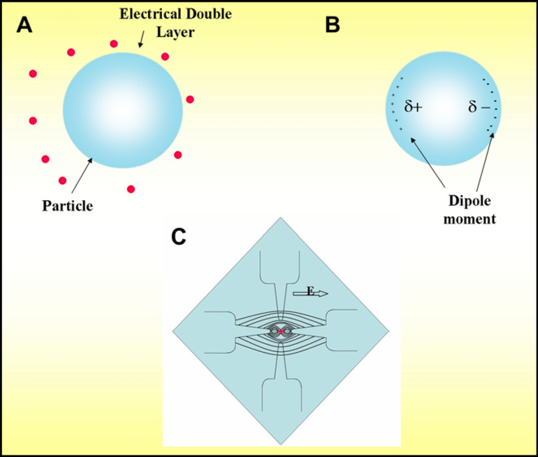
When a particle associated with an intrinsic negative charge (generated by the permanent bonds of the surfactant) is suspended in aqueous medium, its motion can be controlled by the application of homogenous fields. This occurs due to the formation of an electric double layer around it. We use this principle to accurately pattern microparticles creating highly ordered arrays “MicroBridges.” Electrical patterning enables repeatable and rapid alignment of microparticles. This can be achieved by electrophoresis. Figure 7 is a schematic representation of Electrophoretic Principle.
Formation of the polystyrene “Microbridge.”
Polystyrene Bead Properties
Polystyrene beads are manufactured by a method of emulsion polymerization using surfactants. The surfactants used are generally negatively charged sulfates or sulfonates which adsorb onto the surface of the polymer microsphere. Such surfactants modify the surface properties of the polymer spheres by imparting a negative charge around the surface. A gentle washing step is used in the process to clean the surfactant off the microsphere surface using DI water. Polystyrene beads are subjected to alternating steps of washing and centrifuging to remove excess surfactant from the surface. This cleaning step is used to create more spaces on the polymer surface thus enhancing coupling of proteins on the surface via physical adsorption. However, certain permanent sulfate bonds remain on the surface of the bead even after the wash step (Tech Notes 201 Bangs Labs).
Formation of “Microbridge”
When homogenous fields are applied across the electrodes, the electrical double layer on the polystyrene beads gets rearranged to form a dipole across each bead. The dipole moment of the beads allows them to get aligned between the two electrodes under the influence of the electric field emitted by them. The electrokinetic principle of electrophoresis 3 is used to align the surface-charged polystyrene beads to form a bridging structure between the two electrodes. Electrical alignment of beads is preferred to fluidic alignment because electrical patterning of beads is completely repeatable and rapid and can be used to accurately create highly ordered microarrays. A homogenous voltage of 2.1 V applied across the electrodes is used to attract the polystyrene beads closest to the emitted electric fields and rapidly form a bridge structure within 120 s. The polystyrene beads are trapped in their respective positions of the “Microbridge” under the influence of the electric fields. Figure 8 elaborates the formation of the “Microbridge” through the controlled movement of antibody-functionalized polystyrene microspheres.
Electrophoretic principle (A) formation of electrical double layer around the particle, (B) formation of electric dipole in the particle, and (C) application of DC field and formation of electric field lines across the microelectrode platform resulting in controlled particle movement.
Protein Detection
The protein under test (CRP) is detected using a capture system. The polystyrene beads are saturated with the protein receptor (antibody anti-CRP; EMD Biosciences). This yields a baseline signal of 0.412 V. The addition of the test sample containing the antigen CRP to the “Microbridge” of the antibody-saturated beads causes the binding of the antibody to the antigen resulting in the formation of an immunocomplex. The formation of this immunocomplex causes a shift in the DC voltage by 20 mV for a 10-mg/mL concentration of the antibody-saturated polystyrene bead surface. The DC voltage changes are thought to occur due to the variations of the surface charge on the polystyrene bead caused by the formation of the immunocomplex. Bioelectronics involves the coupling of biological agents to electronic support entities which act as a whole system required to generate measurable signals from the analyte of interest. An attempt is made to briefly explain the process of electron conduction through proteins. 5 Protein conductivity through mobile charge carriers such as electrons is said to occur through electron-localizing groups in proteins encompassing energy limits of around 2 eV (electron volt). 6 The dual property of an electron to behave both as a wave and a particle allows it to “tunnel” through the protein's localizing sites despite its insulating feature. The electronic propagation through the proteins is termed as super exchange 7 –9 which explains that the probability of finding a tunneling electron between the energy orbitals of the protein is extremely low but not zero. The electrons emitted due to the formation of the immunocomplex are electrically wired through the various aligned protein-functionalized structures which mediate electron transfer to the microelectrodes. Similar examples of obtaining signal output from electrodes is being used in enzyme-supported electron-mediated transfer in glucose sensor systems 5 where the redox units linked to the electroactive polymer electrically wire the redox center of the enzyme with the electrode. The current generated due to the tunneling electrons can be captured by the sensitive electronic measuring equipment, attributes to the signal increase from the baseline signal as observed in the output signal. Graph 1 indicates significant detection of the analyte in the lower milligram/milliliter range and linearity is observed in the dynamic range.
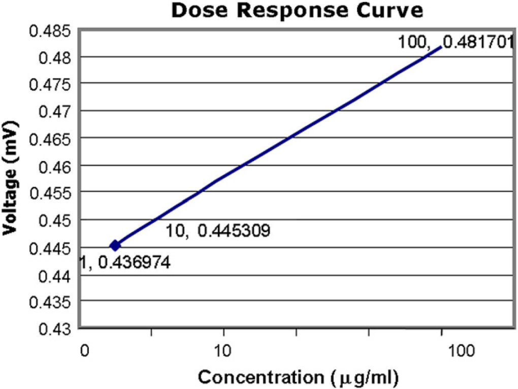
Detection data: Graph depicting an amplification of the signal captured during the Anti-CRP-CRP binding event. The bass signal is obtained from the Anti-CRP functionalized “microbridge”. Linear detection is observed in the microgram/ml range.
Future Work
Commercial immunoassay techniques require careful and long sample preparation times. Immunoassays which use antibody–antigen complex to form immunocomplexes to measure the presence of a specific analyte in the sample. All immunoassay techniques use labeled antibody or antigen to generate a measurable signal in the form of light or change of color in the solution that corresponds to the concentration of the analyte. Immunoassays are highly sensitive and detection speeds are of the order of several hours. Electrokinetically aligning the polystyrene protein supports to form ordered arrays to rapidly detect proteins is the highlight of this research endeavor. We propose to implement the principle of dielectrophoresis to create ordered microarrays. The bead-based assay system dealt with in this article is only a proof of concept device and we aim at improving the limit of detection at lower concentrations of the analyte and also addressing issues of multiplexing and using real blood samples. Multiplexing can be achieved by electrically constructing multiple “Microbridges” across the electrode array for detection of multiple biological agents where each bridge structure behaves as an agent for detection of one specific protein. The photolithographical process of fabricating the base MEA consumes very cheap material which are easily available and takes less than 10 min to manufacture one chip. A batch of 15 chips can be easily manufactured under clean room conditions of Class 100 in less than an hour if planning is done thoroughly. On a further note, this technology has commercial viability and can be manufactured on vast scale for consumption. Analogous to the commercially available glucose meter's test strip, MEA chips are cheap and can be mass produced which can hold a miniscule volume of sample blood. While the measuring and analysis electronics are integrated onto one single system, the entire setup can act as a self-monitoring device which can detect the amount of analyte present in the patient's blood. This micrototal analysis system which is rapid, label-free, sensitive, and selective can be used to detect major diseases if the corresponding combination of disease biomarkers is detected.