
Abstract
A fully automated electronic microarray control system (Nanochip 400 System) was used to carry out a combinatorial process to determine optimal conditions for fabricating higher order three-dimensional nanoparticle structures. Structures with up to 40 layers of bioderivatized nanoparticles were fabricated on a 400-test site CMOS microarray using the automated Nanochip 400 System. Reconfigurable electric fields produced on the surface of the CMOS microarray device actively transport, concentrate, and promote binding of 40 nm biotin- and streptavidin-derivatized nanoparticles to selected test sites on the microarray surface. The overall fabrication process including nanoparticle reagent delivery to the microarray device, electronic control of the CMOS microarray and the optical/fluorescent detection, and monitoring of nanoparticle layering are entirely controlled by the Nanochip 400 System. The automated nanoparticle layering process takes about 2 minutes per layer, with 10–20 seconds required for the electronic addressing and binding of nanoparticles, and roughly 60 seconds for washing. The addressing and building process is monitored by changes in fluorescence intensity as each nanoparticle layer is deposited. The final multilayered 3D structures are about 2 μm in thickness and 55 μm in diameter. Multilayer nanoparticle structures and control sites on the microarray were verified by SEM analysis.
Introduction
A key grand challenge in nanotechnology is the development of fabrication technologies that will lead to cost-effective nanomanufacturing processes. In addition to the more classical top-down processes such as photolithography, the so-called bottom-up processes are also being developed for the self-assembly of nanocomponents into higher order structures, materials, and devices. 1 –6 To this end, considerable efforts have been carried out on both passive and active types of layer-by-layer (LBL) self-assembly processes as a way to make three-dimensional layered structures which can have macroscopic x–y dimensions. Generally, most processes involve dipping an activated substrate material (electrostatic charged, chemically reactive, etc) into a solution which contains a macromolecule, polymer, or nanoparticle with an opposite charge or reactivity to the substrate material. The reaction is given some time to complete, the substrate is washed extensively, and then the next layering step is carried out. 7 –28 Unfortunately, limitations of many of these present LBL self-assembly processes provide considerable incentive to continue the development of better paradigms for LBL nanofabrication, heterogeneous integration, and in particular, the automation of these processes.
Over the past decade, electronic microarray devices produced by a top-down photolithography process have been developed for DNA diagnostic applications. In these applications, electronic microarray devices which produce re-configurable electric fields on their surfaces are used to address and bind negatively charged biotinylated DNA molecules to selected test sites on the microarray surface. Subsequently, samples containing unknown DNA sequences are then rapidly transported and selectively hybridized to the DNA sequences bound at the specific test sites. 29 –37 Thus, these devices are able to direct and accelerate the self-assembly or “bottom-up” process of DNA hybridization occurring on the microarray. In addition to the directed transport and addressing of biomolecules, the ability of electronic microarrays to carry out the rapid patterned deposition of charged nanoparticles was also demonstrated early in the development of the technology. 30 Ultimately, electronic microarrays have been used to carry out transport, addressing, and selective binding of a variety of charged biomolecules such as DNA, RNA, biotin/streptavidin, and antibodies 40 ; nanoparticles 30 , 41 ; cells 42 ; and even 20-μm-sized light-emitting diode (LED) semiconductor devices. 38 , 39 , 43 , 44 These devices have been shown to manipulate a surprisingly large variety of entities that range in size from small molecules to micron-scale objects. 45 –52
Electronic arrays have several important features that make them attractive for assisted self-assembly nanofabrication. First, a permeation layer or porous hydrogel is used to cover the microelectrode structures on the array. The permeation layer is usually impregnated with streptavidin which allows biotinylated DNA (antibodies, nanoparticles, etc) to be bound at the selected site. This layer also allows relatively high DC electric field strengths to be used for rapid electrophoretic transport of molecules and nanostructures, while protecting the more sensitive DNA, proteins, or nanostructures from the adverse effects of the electrolysis products generated at the electrodes. 29 –37 A second feature of electronic array devices is that they can be designed in a wide variety of shapes and sizes. To date, arrays have been fabricated in sizes from 2 mm × 2 mm to over 2.5 cm × 2.5 cm, with 25–10,000 electrodes and with electrode structures which range in size from 10 μm to several millimeters. A third feature is that sophisticated complimentary metal-oxide semiconductor (CMOS) control elements can be integrated into the underlying silicon structure of electronic microarrays which allows precise control of currents and voltages to each of the individual microelectrodes on the array. Finally, significant size reduction in the electronic array controller system (Nanochip 400 System) provides a relatively compact control unit for carrying out a fully automated process for LBL-directed self-assembly nanofabrication. Using the fully automated Nanochip 400 System, bread-board (B-B) controller system, and 400-test site CMOS microarray devices, we have now demonstrated a rapid and highly parallel combinatorial process for directed self-assembly of bioderivatized nanoparticles into higher order multilayered three-dimensional structures.
Automated Nanochip 400 System
Nanofabrication Technologies
Current nanofabrication technologies do not provide a satisfactory palette of methods to effectively produce materials with combined properties, for example, ionic conductivity, electronic conductivity, or structural mechanical properties that use new nanophenomena discovered in materials such as quantum dots, carbon nanotubes, dendrimers, or a combination of these materials. A predominant bottom-up method is self-assembly, in particular based on DNA (started by Seeman's group 53 ) or amyloid fibrils, where fabrication is performed using the attachment of specific sticky ends of DNA to create branched junctions in molecular structures. 53 These methods are prone to random errors because the assembly is controlled by diffusional or crystallization processes where no precise external control or force is imposed atomic force microscope (AFM) and scanning tunneling microscope (STM) technologies have been used for precise deposition or removal of molecules on the surface, and NanoInk has commercialized Dip-Pen Nanolithography that enables building patterns, layers, or structures with nearly any molecule at resolutions down to 10 nm. This technology is limited only to small surface area patterning. Next-generation lithographic technologies could provide fabrication of nanostructures or devices at a larger scale, but at high cost and with only limited number of molecules used in the assembly. ASML and Nikon are already shipping immersion lithography systems for 45-nm half-pitch production. 55 Extreme ultraviolet lithography, backed by Intel, uses 13.5 nm wavelength UV light to extend optical lithography. Electron beam lithography uses shorter wavelength and offers best resolution, however, its high complexity and low throughput are serious drawbacks in fabricating larger structures or generating sizeable materials. Nano Imprints developed the nano-imprint lithography where imprints or stamps of desired structures are directly transferred onto a wafer in steps. The company is foreseeing future resolution well beyond 45 nm, but the size and diversity of produced structures is limited. One of the major drawbacks of current nanofabrication technologies is that they are not designed for interfacing nanostructures with micro- and macroscale elements or materials. The method described here provides easy interfacing to higher structures and combining various properties within the created materials.
The NanoChip 400 System—An Electronic Microarray System That Combines Automated Fluidics and Electrophoretic Assembly of Molecules and Nano-Elements
The NanoChip 400 System is designed to integrate (Fig. 1) advanced microelectronics and molecular biology into a platform technology with broad research applications, and with potential commercial applications in the fields of biomedical research, genomics, genetic testing, drug discovery, and diagnostics. The application described here enables bottom-up directed assembly of nano-elements, such as (bio)mole-cules (e.g., DNA, proteins, dendrimers, and fullerenes), nanoparticles, nanotubes, including carbon nanotubes, organic and/or inorganic wires, or conducting and semiconducting elements into assemblies or functional devices. The system consists of the following main components: NanoChip 400 Instrument, NanoChip 400 Cartridge, Fluidics Cartridge, NanoChip 400 Software, and PC Workstation. This fully automated general-purpose system, which incorporates a proprietary 400-test site CMOS electronic microarray (with 400 50-μm-diameter microelectrode test sites), provides a flexible tool for the quick identification and analysis of test samples. It presents an open platform that can be used by the users to combine various fluidics functions, such as dispensing reagents, samples, or washing and buffer solutions and an electrophoretic addressing of the nanocomponents of interest that enables precise, controlled, and accelerated transport on the electronic microarray.
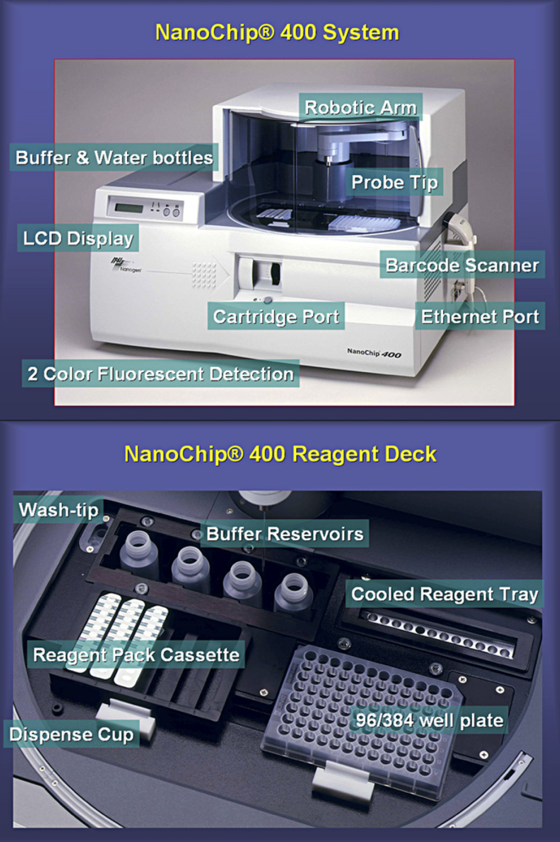
NanoChip 400 System exterior (top) with reagent and chip access points visible. The sample regions (bottom) are shown with various types of sample wells.
The system has fluorescence, LED-based optical component which is used to verify, detect or measure binding between different assembly layers, or a capture and a target system (used in medical or biological applications), for example, a specific capture DNA with a nanoparticles or carbon nanotube labeled with appropriate complementary oligonucleotide. Reporting is performed using fluorescently labeled oligonucleotides. The red excitation wavelength is 626 nm and emission wavelength is 668 nm. The green excitation wavelength is 525 nm and emission wavelength is 553 nm.
Figure 2 demonstrates the principle of operation of the instrument and how a robotized fluid transport is combined with high precision electrophoretic transport which enables a very low number of molecules to be rapidly transported by the electric field applied between the microarray electrodes. In essence, the user can define a software-based protocol that takes fluid samples, reagents, or nanocomponents for assembly from the microtiter plate and addresses them in accordance to the user defined order onto particular locations (test sites) on the microarray. The addressing comprises electrophoretic transport from the bulk solution above the microarray (ca 30 μL) to one or more array test sites. The hydrogel permeation layer covering the array serves for binding of the first or capturing layer. Subsequent layers are bound using molecular conjugation mechanisms, such as DNA hybridization, biotin–streptavidin, or similar binding mechanism. Figure 3 shows how microliter volumes of reagents, probes, samples, or more generally, nanocomponents are fluidically transported using a robotic arm to the 400-site CMOS microarray packaged in a cartridge (Fig. 2) where further transport and manipulation are performed electrically by controlling voltages and/or currents on each individual electrode. The electrophoretic transport enables rapid, highly directional movement of desired molecules toward electrodes with micro- and/or nanoprecision. This electrophoretic addressing, deposition, and binding process occurs within seconds. The main advantage of this approach is that no masks, as in photolithographic methods are needed between addressing and depositing different layers in the assembly process.
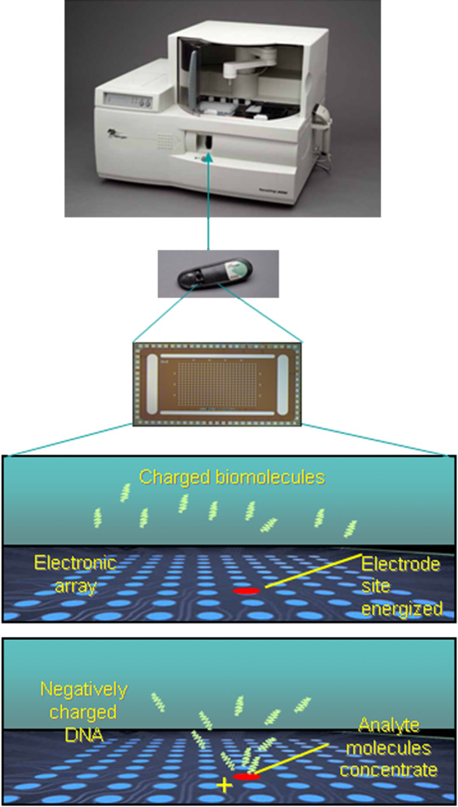
NanoChip 400 System (top) with NanoChip cartridge device (middle top), containing the 400-site CMOS electronic microarray (middle bottom). The schematic drawings (bottom) demonstrate the electrophoretic addressing on the microarray where directional electrophoretic transport is used for assembly of molecules, nanoparticles, and/or other nanocomponents (here DNA is used as an example). Charged (and noncharged) nanocomponents, biomolecules, such as negatively charged DNA, are electrophoretically attracted to the positively biased microelectrode. Transport of DNA occurs very rapidly (within seconds) at the microelectrode test site, enabling binding to molecules (DNA, biotin, and streptavidin) already present at the site.
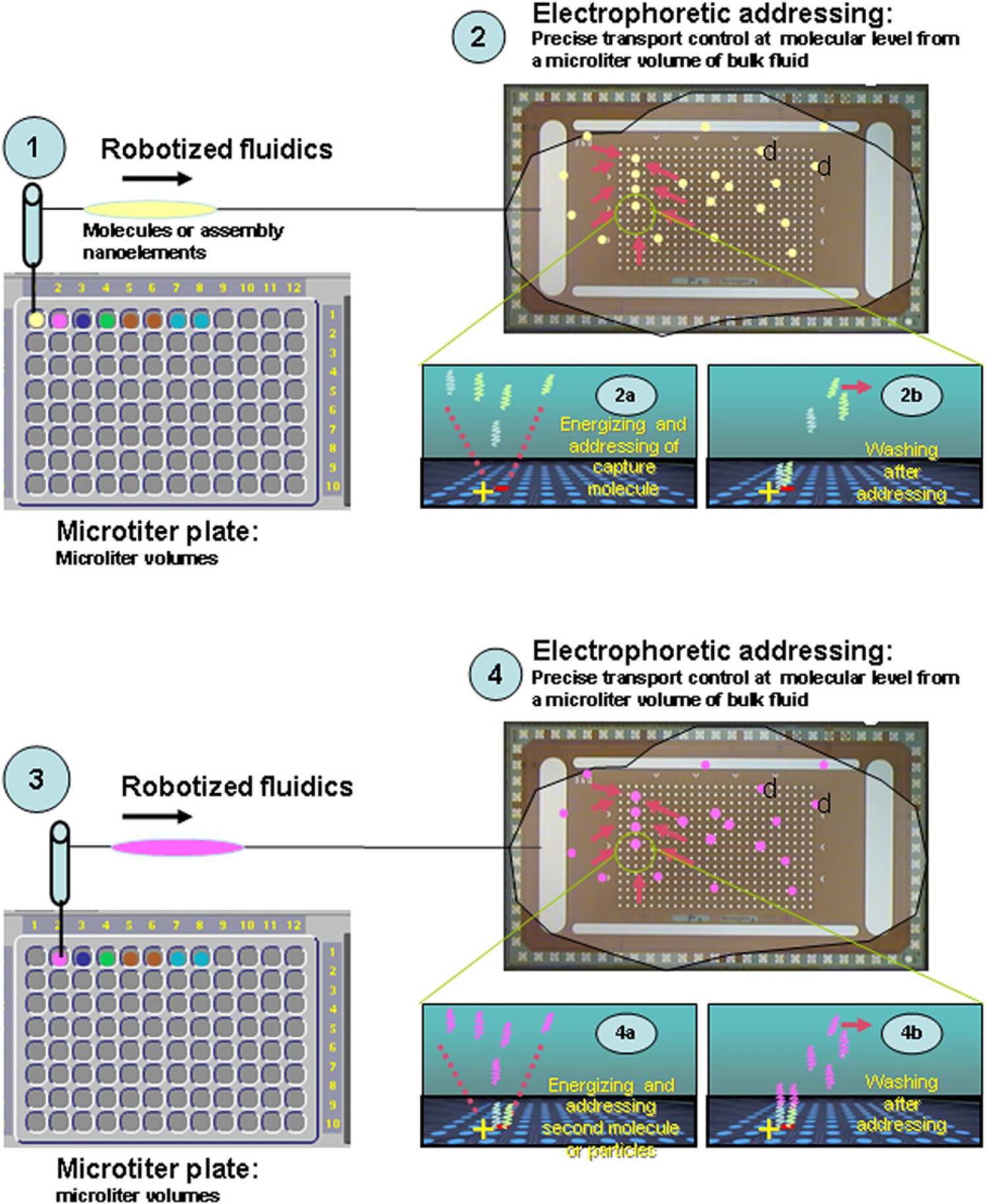
Schematic diagram of the automated operation used in the NanoChip 400 System that can provide directed self-assembly of various nanocomponents, for example, molecules, nanoparticles, carbon nanotubes, metallic/semiconducting nanotubes, dendrimers, and fullerenes on the electronic microarray. The operation provides easy combination of robotized fluidics (user input through a microtiter plate) and electrophoretic addressing: (1) a microliter volume solution of assembly element 1 or molecule 1 is transferred through a robot needle to the array; (2) particular locations on the array are energized and molecules are addressed electrophoretically to a desired position or electrode (2a); excess reagent 1 is washed away; (3) a second assembly element or second molecule is transferred through robotized fluidics to the array and addressed (4a); the secondary molecule binds to the first, for instance, through one of the conjugation mechanisms, for example, in the case of DNA binding, by hybridization. Excess reagent is washed away from the array (4b); the robotized fluidics and electrophoretic steps are repeated sequentially until the desired structure, device, or assembly is formed on the array.
An important feature for optimization of the self-assembly structures and achieving repeatability of the protocols is broad access to viewing various parameters measured during the experiment through cartridge data and cartridge session data. The user needs only to select the title of a protocol from the protocol tree that displays cartridge session data views. These views may include the following: materials configuration information (including sample names and reagent locations); calibration images (for optics calibration); any protocol error messages or warnings generated (for troubleshooting); raw fluorescence images and values (for comparison with processed images); pad activation information (for micro-electronic activity of test sites); thermal history (for temperature changes); and optics contact sheet (including all images taken during the session).
The 400-site CMOS microarray platform is an open platform and users can choose their application, thus over 200 assays have been developed by the users with medical and biological applications where the electrophoretic transport is used for accumulation and concentration of target DNA, rapid electronic hybridization, and reporting of the analyte molecules. In the research lab, other entities–peptides, proteins, antibodies, enzymes, cells, and biopolymers–have been transported to specific locations on the array. Inorganic components including most types of polymeric or metallic nanoparticles, quantum dots, and even micron-scale LEDs can also be addressed and positioned on the array. Thus, this sophisticated “electronic addressing” technology can be used to place a variety of nanoscale and microscale components at specific positions and integrate them into molecular, nanoelement and/or microstructures.
Because the transport can be simultaneously controlled at large numbers of electrodes, the platform offers integration of nanoscale precision fabrication with micro- and macroscale assembly. Relatively large structures, potentially in the range of centimeters could be manipulated using larger arrays. Three dimensional molecular and nano-element structures can be made by linking together molecules using conjugation techniques such as DNA hybridization, which has been demonstrated on carbon nanotubes, quantum dots, and other nano-elements.
Nanocomponents and Directed Self-Assembly Fabrication Method
The basic goal of this work was to use the automated NanoChip 400 System to carry out in a combinatorial fashion the electric field-directed LBL self-assembly of biotin and streptavidin 40-nm fluorescent nanoparticles into higher order structures. The goal was to test the addressing and deposition parameters of time and DC currents across the microarray, and to do so in a completely automated manner. By automating the dispensing and washing steps, it is possible to remove process variations brought about by manual depositions. Furthermore, by automating the process variations by running the microelectrodes in parallel, it is possible to quickly test a large number of addressing and deposition parameters by direct comparison. Figure 4 shows the basic scheme for carrying electric field directed LBL self-assembly of biotin and streptavidin 40 nm fluorescent nanoparticles into multilayered structures.
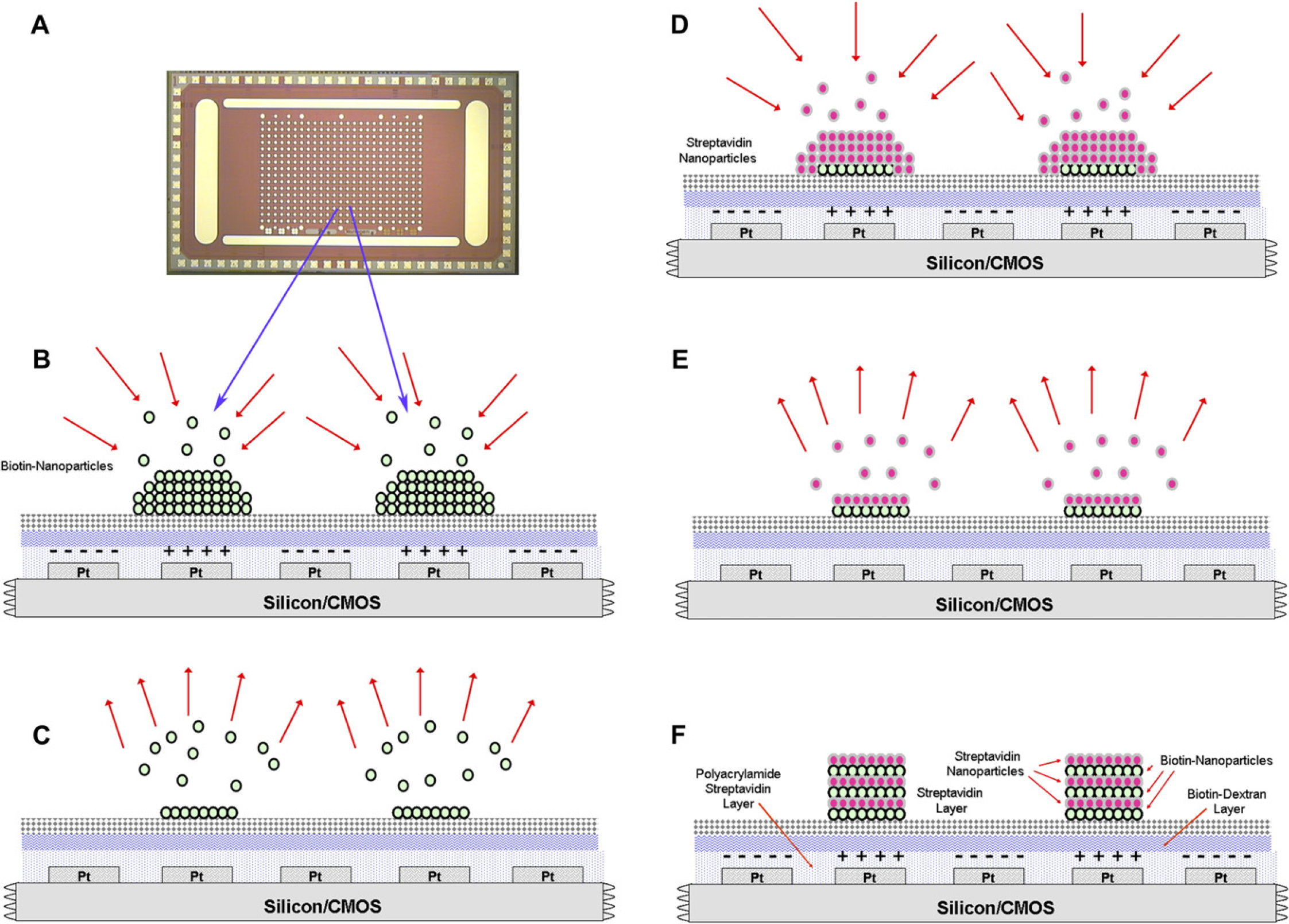
The typical workflow process is shown. Starting with a new CMOS microarray (A), biotin particles are electrophoretically pulled down to a streptavidin surface (B), and then excess particles are washed away (C). Next, streptavidin particles are pulled down to the previously deposited biotin particles (D), and then excess particles are washed away (E). The process is repeated multiple times to build up a larger number of layers (F).
The typical workflow for the directed self-assembly of nanoparticles involves (1) initial microarray preparation, (2) nanoparticle deposition and monitoring, and (3) final microarray cleanup. The entire workflow is programmed in advance and involves a series of commands to pump, wash, activate the microelectrodes, and monitor the nanoparticle layering results. In this work, we make use of biotin and streptavidin bonds to link the nanoparticles. The biotin/streptavidin system is a high strength, high specificity affinity bond which can be used to attach to larger systems. A nanoparticle containing a biotin coating will rapidly and strongly bond to a streptavidin nanoparticle or a surface covered in streptavidin (see Fig. 4). The 400-site CMOS microarray at the core of the Nanogen 400 system contains a 10-μm-thick polyacrylamide gel layer with streptavidin bound throughout. This gel layer is used to protect any fabricated structures from direct contact with the electrodes and to provide a binding surface. To prepare the surface for binding with functionalized nanoparticles the system performs three steps. First, the microarray is washed and hydrated in deionized (DI) water to remove protective layers on the microarray and to prepare the hydrogel for use. Second, a solution of biotin dextran (2 μM, Sigma Aldrich B9264) in DI water is flowed onto the microarray and allowed to hybridize for 30 min, after which the microarray is washed to remove excess solution. This coats the microarray with a biotin surface. Third, a solution of streptavidin (10 μM, Roche 11721666001) is flowed onto the microarray for 30 minutes to bind to the biotin dextran and give the microarray a more uniform and complete streptavidin surface. After this, the microarray is washed with 100 mM l-histidine to remove excess streptavidin solution and to prepare the microarray for nanoparticle deposition. After the preparation step, the microarray is then ready for nanoparticle LBL fabrication. A dilute solution of yellow-green fluorescent biotin 40 nm nanoparticles (0.5 nM, Invitrogen F8766) in 100 mM l-histidine is removed from a sample holding well and pumped onto the microarray. All the desired electrodes on the microarray are then activated simultaneously at various time and currents. The typical activation parameters for electrodes are current ramps between 0.025 and 0.4 μA in 0.025 μA increments and activation times of 10, 15, 20, and 30 seconds. Each condition is repeated multiple times across the microarray to monitor spatial uniformity and repeatability. When activated, the charged nanoparticles in solution are pulled down to the microelectrode surfaces in proportion to the time and current of activation. The microarray is then cleaned of excess solution and unbound nanoparticles with an l-histidine wash, and a fluorescent image is taken to monitor the nanolayer fabrication progress. After the deposition of a layer of biotin nanoparticles, the process is repeated with the next layer of nanoparticles. The deposition methods and parameters are identical except for the nanoparticles used, which are red fluorescent streptavidinated 40 nm polystyrene nanoparticles (0.5 nM, Invitrogen F8770). After deposition, the microarray is washed as it was with the biotin nanoparticles. To fabricate a larger number of layers to build a more complicated multilayer structure, the processes were simply repeated. By alternating the depositions of biotin and streptavidin nanoparticles, we have been able to create structures with up to 40 layers.
Results
Nanoparticle layer growth was monitored by fluorescent imaging. Brighter fluorescent signals on an electrode are taken to have a greater amount of nanoparticles. As seen in Figure 5, as current and time of deposition increase, so does the intensity of the fluorescent signal. The signal is a strong function of the total applied charge. There is a minimum particle deposition cutoff for layer growth. Without enough nanoparticles being deposited in one layer, there are not enough binding sites for a subsequent layer to form. This is manifested as pads that are electronically active but with no layers being formed. The total charge is a function of both the current at each electrode, and the time of deposition. Figure 6 shows scanning electron microscope (SEM) results of both inactivated and activated electrodes. The entire chip surface is covered with a streptavidin-functionalized surface, and is equally susceptible to nanoparticle binding. As seen in Figure 6a, even after 40 layers of deposition elsewhere on the chip there is only a small amount of background nanoparticle binding. Conversely, on regions like in Figure 6b, where nanoparticles have been addressed multiple times there is a thick layer with no gel surface visible. The difference between inactivated control and activated experimental rows can be seen in Figure 6c. The dependence of particle layering on applied current and time is shown in Figure 7, with layer growth increasing monotonically with both increased time and current. A cross section of the deposited nanoparticle layers is shown in Figure 8, demonstrating that more than a single layer of particles has been deposited.
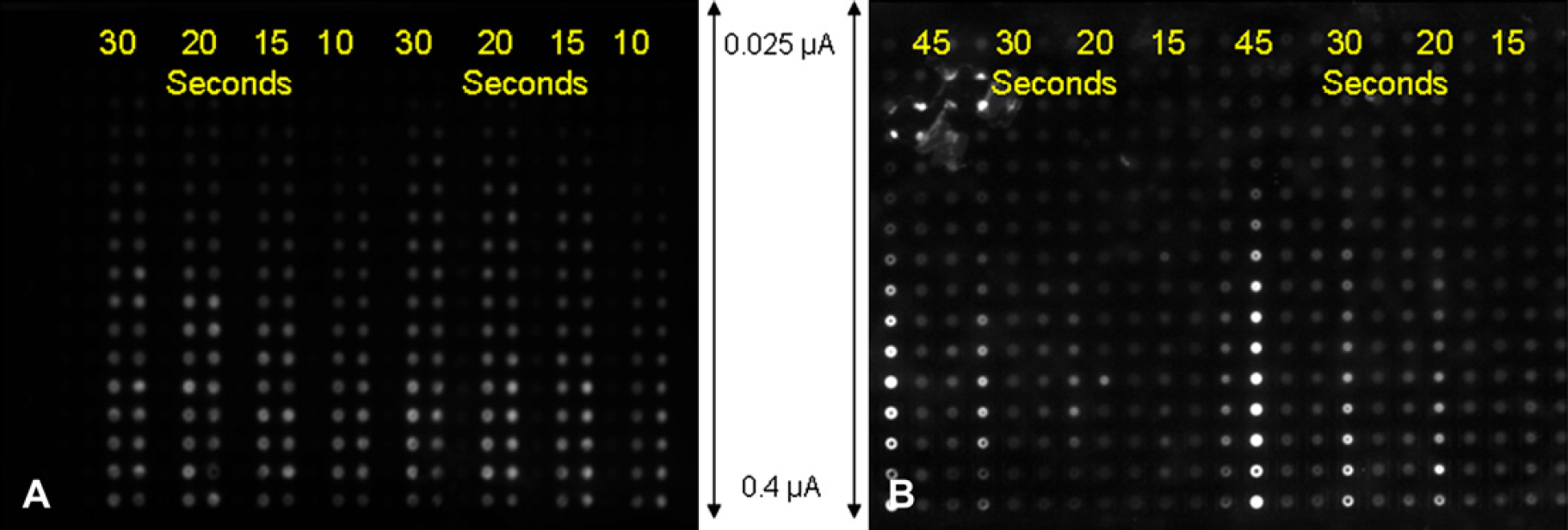
Fluorescent images of layers of nanoparticles for various times and currents of deposition. The left side is an image taken from the fully automated Nanogen 400, and shows a current ramp from 0.025 to 0.4 μA, and times of deposition from 10 to 30 s. The right image is taken from a nonautomated benchtop system which has identical electronics but no fluidic automation. The images are taken after 20 layers of deposition.
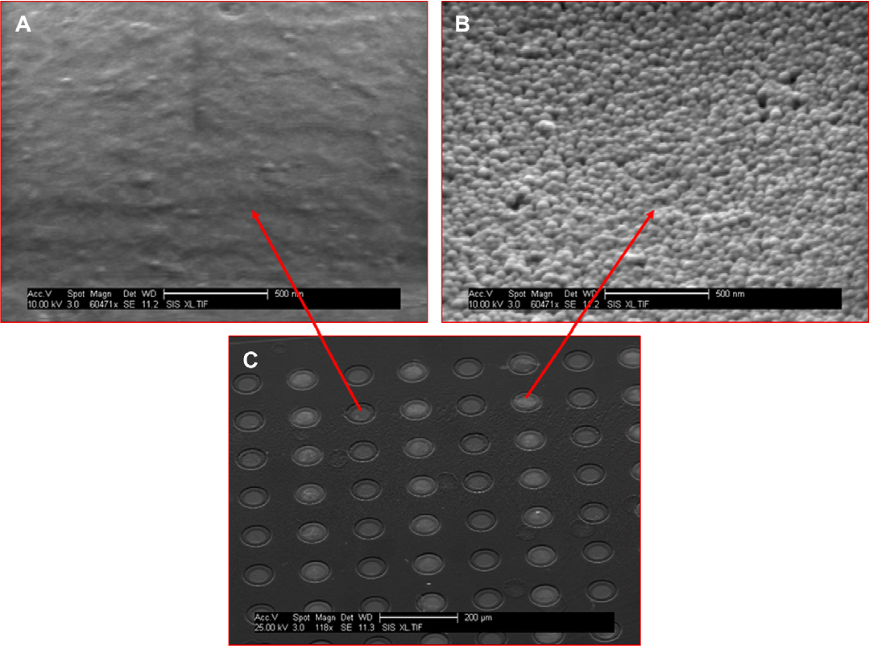
(A) An SEM image of a CMOS microarray surface which has not been activated electronically, but has been functionalized and exposed to a nanoparticle solution. Only a small amount of background particle binding is visible. (B) A section from the same chip which has been electronically activated multiple time to grow layers. The electrode surface is fully covered with nanoparticles. (C) An SEM image of multiple electrodes of the same chip, some being activated, and others not. The CMOS microarray used for these images was taken from a B-B system.
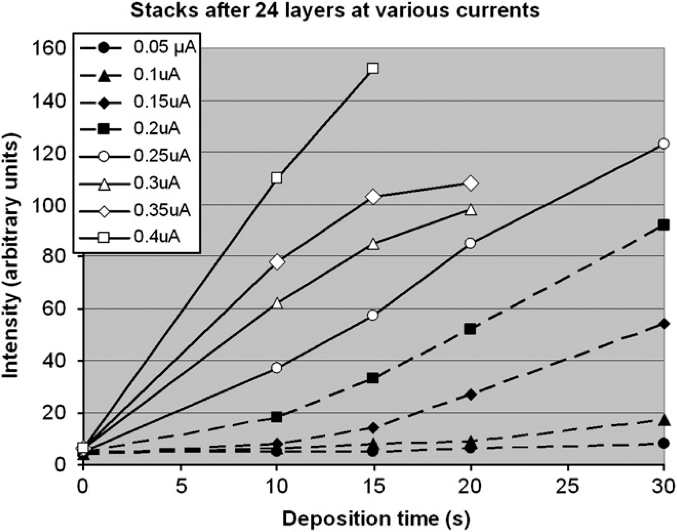
A plot showing the relative fluorescent intensity for nanoparticle layering on the microelectrodes at the various deposition times and current levels for 24 layers.
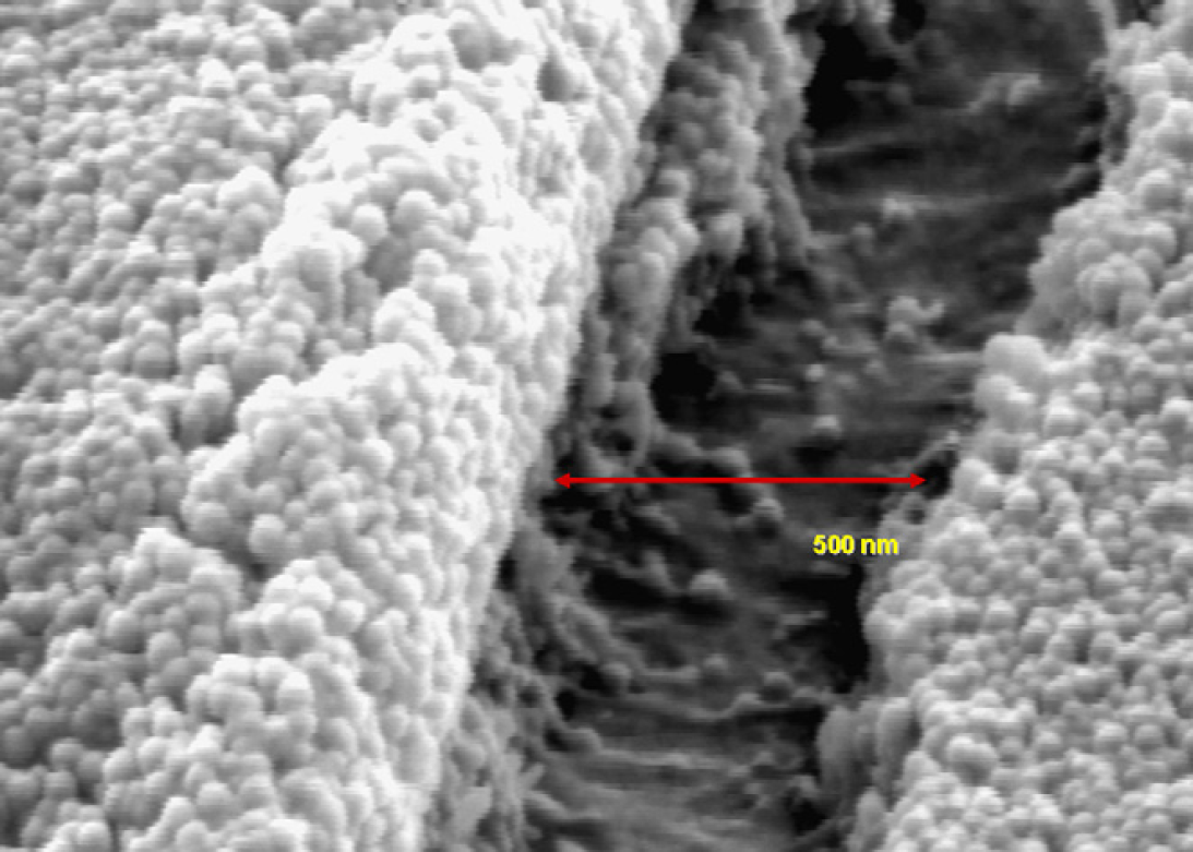
An SEM cross section through multiple layers of biotin and streptavidin 40-nm nanoparticles that have been assembled on a single electrode of the microarray. The 500-nm line is provided for scale.
Discussion and Conclusions
We have shown that automated electric field-directed self-assembly nanofabrication of 40-layer bioderivatized nanoparticle structures could be carried out in a rapid and highly parallel format using a Nanochip 400 Controller System and CMOS electronic microarray devices. Combinatorial type experiments carried out on the CMOS microarrays were used to determine optimal conditions for nanoparticle layering. Highly efficient nanoparticle addressing, deposition, and binding could be achieved in 10–20 seconds or less. With washing steps of about 60 seconds, the total time for creating a nanoparticle layer is about 2 minutes Thus, the 40-layer nanoparticle structures could be completed in less than 2 hours. The optimal electronic addressing window for creating high-quality 3D layered structures appears to be at current levels in the 0.25 to 0.35 μA range. Because the nanoparticles used in our experiments were of the same size (40 nm), it is difficult to determine from the SEM image (Fig. 8) the homogeneity of individual biotin and streptavidin nanoparticle layers within the multilayered structures. When taken together with fluorescent monitoring of depositions, and the experiments showing no layering of similar nanoparticles, the SEM images are consistent with a 40-layer alternating nanoparticle structure. Work is now in progress with different sized nanoparticles to better determine true quality of individual layers within the multilayer structures.
The results of these experiments have demonstrated a number of advantages relevant to 3D self-assembly LBL nanofabrication. First, it was shown that high electric field strengths and electrophoretic transport from the bulk solution could be maintained even through many layers of nanoparticles, allowing the new upper layers of nanoparticles to still be rapidly addressed to the activated sites. Second, our results showed that the integrity of the biotin–streptavidin ligand binding was maintained even after 40 layers of nanoparticles were addressed. This is extremely important for any 3D self-assembly process that is based on biomolecular binding using highly specific protein or DNA ligands. This ability to use high electric field strength with minimal side effects is most certainly due to the permeation layer which separates the electrode from the nanostructures, and due to the relatively short addressing times (5–15 seconds) needed for nanoparticle addressing and deposition. Third, because the high electric field strengths produce enormous concentration effects at the activated sites, only minimal concentrations of nanoparticles were needed for addressing and deposition. In fact, the concentration of nanoparticles used was so low that no significant nonspecific binding of nanoparticles occurred during the whole process. Fourth, CMOS electronic array devices appear to allow nanoparticle layering to be carried out much faster (one to two orders of magnitude) than comparable passive LBL self-assembly nanofabrication processes. Finally, a fully automated nanofabrication process including nanoparticle reagent delivery to the CMOS microarray device, electronic control of the microarray, and the optical/fluorescent detection and monitoring of nanoparticle layering process could be carried out using the Nanochip 400 System. We believe that the use of the controller system and CMOS electronic microarray devices for directed self-assembly represents a unique example of combining the best aspects of “top-down” and “bottom-up” technologies into a potentially useful nanofabrication process. Such a process may allow the assembly of integrated nano/micro/macrostructures for a variety of bio/chemsensor, nanoelectronic, nanophotonic, and nanomaterials applications.
Acknowledgments
We thank the National Science Foundation (NSF) for funding related to NSF award no. DMI-0327077; and to Nanogen for funding and supplying CMOS microarrays and the Nanochip 400 System.