
Abstract
The straight and curved gallium nitride (GaN) nanowires were successfully synthesized by controlling the gallium/nitrogen reactant ratio via a chemical vapour deposition method. The structure and morphology of nanowires were characterized by X-ray diffraction (XRD), transmission electronic microscopy (TEM), field emission scanning electron microscopy (FESEM), selected area electron diffraction (SAED) and high resolution transmission electron microscopy (HRTEM). The straight and curved GaN nanowires are composed of wurtzite and a zinc blende structure, respectively. Photoluminescence (PL) spectra of zinc blende GaN nanowires showed a strong UV emission band at 400 nm, indicating potential application in optoelectronic devices.
1. Introduction
A one-dimensional (1D) nanostructure composed of GaN has attracted tremendous attention due to its unique optoelectronic properties, high mobility and excellent thermal stability [1–2] in the synthesis of semiconductor devices, typically as field effect transistors, light-emitting diodes, logic circuits, UV photodetectors and nanolasers [3-7]. So far, various 1D nanostructures of GaN have been successfully synthesized via different routes by using catalyst mediation techniques, such as chemical vapour deposition (CVD) [8], template direct methods, which use carbon nanotubes [9] and porous alumina as scaffolds [10], or catalyst-free techniques, including laser ablation [11], molecular beam epitaxy (MBE) [12], metalorganic chemical vapour deposition (MOCVD) [13] and hydride vapour phase epitaxy (HVPE) [14].
Recent years have seen a growing interest in the synthesis of GaN nanowires with different sizes and morphologies, such as nanowires [15], nanowire arrays [16], zigzag-shaped nanowires [17], leaf-shaped nanowires [18,19] and etched GaN nanowires [20]. Most of these studies are focused on common hexagonal wurtzite GaN nanostructures because they are stable under thermodynamics. The formation of the metastable cubic GaN is difficult to synthesize under thermodynamic equilibrium conditions. However, the cubic GaN has advantageous physical properties compared to those of the hexagonal GaN due to easier p-type doping and easier cleaving for laser facets. The pure cubic GaN nanowires have not yet been produced. Here, sun-shaped high-quality single crystalline GaN nanowires, with a diameter of 15–100 nm and a length of up to several hundred micrometres, were fabricated through a facile catalytic CVD. The pure cubic GaN nanowires were prepared for the first time.
2. Experimental Section
CrCl3.6H2O (0.266g) was dissolved in ethanol (10 ml). A mixture of CrC13.6H2O (1.0ml.) ethanol solution and iron powder (0.01 g) was stirred ultrasonically for 15 min. This mixture of chromium and iron ethanol solution was used as a catalyst. The synthesis of the GaN nanowires was carried out in a conventional high temperature horizontal quartz tube furnace. Substrate of silicon (111) was respectively cleaned with deionized water, acetone and absolute ethanol in an ultrasound bath for 15 min. Then, a mixture of chromium and iron ethanol solution was dropped on the surface of the substrates of silicon. After drying the substrate at 80 °C in air, the catalysed silicon substrates were placed on the side of a quartz boat loaded with Ga powder (Ga: 99.999%). The distance between the Ga source and the catalysed silicon substrate was between 10 and 50 mm. The quartz boat, containing the Ga source, and the catalysed silicon substrate were placed inside a quartz tube at the centre of a reactor. Prior to heating, the quartz tube was evacuated to less than 0.01 Torr and filled with nitrogen until the pressure was raised to about 1 atm in the tube on three occasions. A carrier gas of nitrogen was kept flowing through the quartz tube at a flow rate of 50 sccm. Meanwhile, the temperature was increased from room temperature to 900 °C at a rate of 5 °C/min. When the temperature was raised to 900 °C, a steady NH3 flow of 200 sccm was started and maintained for 90 min (the N2 gas flow was closed during the reaction). After the reaction, the furnace was cooled to room temperature with N2, with the resulting products collected on the surface of silicon.
The size and morphology of the deposited products were examined directly by FESEM (SEM, Hitachi S-4800). The chemical composition of the products was characterized by energy–dispersive X–ray spectroscopy (EDS) using an EDS microanalysis system (Horiba, 7593-H) attached to an SEM (Hitachi S-4800). Further structure studies of the materials were investigated using a transmission electron microscopy (TEM, Hitachi, model 7700) instrument with an accelerating voltage of 80 kV. High resolution TEM (HRTEM) and selected area electron diffraction (SAED) were performed on a JEM–2010 instrument (JEOL Ltd.) and operated at an accelerating voltage of 200 kV. Optical properties of the samples were analysed on PL measurements using the excitation source of a 300 nm line of an Xe laser (Edinburgh Instruments Ltd., FLS920).
3. Results and Discussion
Figure 1 shows images of the FESEM of two kinds of sun-shaped GaN nanowire samples, which can be controlled by varying the gallium/nitrogen reactant ratio. When the growth occurred in a nitrogen-rich environment, a large number of straight sun-shaped GaN nanowires was obtained. Figures 1(a) and 1(b) show that these nanowires grow divergently around a centre with diameter of 20 to 30 nm and a length of dozens of microns. Furthermore, each nanowire is straight and uniform with a smooth surface. When the reaction condition changes to a gallium-rich environment, the curved nanowires are obtained (see Figures 1(c) to 1(e)). Figure 1(c) is a low resolution image of a single nanowire with a length of about 650 μm. Figure 1(d) shows the typical curved sun-shaped GaN nanowire, with many curved nanowires observable. The high magnification image in Figure 1(e) reveals that these nanowires possess heterogeneous diameters ranging from 20 to 100 nm. To figure out the detailed composition of these sun-shaped nanowires, an energy–dispersive EDS technique was used (inset of Figure 1(c)), which indicates the presence of gallium, nitrogen, iron, cadmium and small amounts of oxygen in the centre of the sun-shaped nanowires.

(a) and (b) are SEM images of straight sun-shaped GaN nanowires; the inset of (b) is the EDS analysis of GaN nanowires; and (c) to (e) are SEM images of curved sun-shaped GaN nanowires
Figure 2(a) shows a typical TEM image of a single nanowire with a diameter of around 20 nm, which is selected from the first sample of straight sun-shaped GaN nanowires. Figure 2(b) is an HRTEM image taken from the ring that is marked as part of Figure 2(a). The lattice spacings of 0.276 nm in the HRTEM correspond to the {10
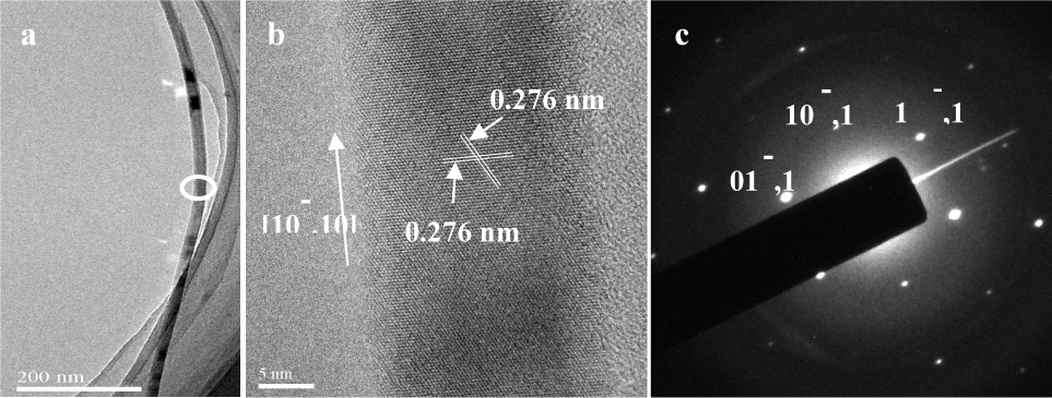
(a) shows the TEM image of straight sun-shaped GaN nanowires; (b) shows the HRTEM image; and (c) shows the SAED pattern of the ring marked partly in (a)
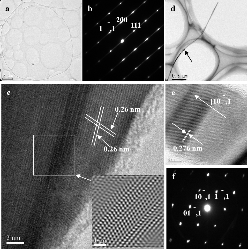
(a) shows the TEM image of a curved sun-shaped GaN nanowire sample; (b) shows the SAED pattern; (c) shows the HRTEM image of the nanowire in (a); (d) shows the TEM image of a single straight nanowire; (e) shows the HRTEM image; and (f) shows the SAED pattern of the nanowire in(d)
In order to characterize the structure of the second curved sun-shaped GaN nanowire sample, a typical individual curved nanowire with a thicker diameter of around 100nm is shown in Figure 3(a). Figure 3(b) shows a typical SAED pattern of this nanowire. From Figure 3(b), the cubic GaN can be indexed with a zone axis of [10
The PL emission spectrum at room temperature of the two kinds of sun-shaped GaN nanowires samples is shown in Figure 4. For the first sample of straight sun-shaped GaN nanowires, a strong emission peak, which was observed at 370 nm (3.35 eV) at room temperature, can be attributed to band-edge-related emission of wurtzite GaN [21] (see line a in Figure 4). In addition, the weak 542nm (2.28 eV) emission is consistent with the yellow luminescence observed in bulk GaN [22], which implied that the GaN nanowires possess high quality and few defects associated with the HRTEM analysis. On the contrary, for the sample of curved sun-shaped GaN nanowires, the emission peak was around 369 nm (3.36eV), which reveals that the band-edge emission of wurtzite GaN is relatively weak. The broad emission peak around 400 nm (3.1eV) indicates the band-edge emission of cubic GaN [23] (see line b in Figure 4). These observations, which illustrate the general existence of such a zinc blende structure of GaN in the curved sun-shaped sample as well as a limited wurtzite structure of GaN, are consistent with the HRTEM analysis.

PL spectra of (a) straight sun-shaped GaN nanowires and (b) curved GaN nanowires
As we all know, the most common growth mechanism for a one-dimensional nanostructure, especially involving semiconductor nanomaterials, is the vapour-liquid-solid (VLS) mechanism, whose obvious feature is the presence of catalyst nanoparticles on the tips of nanowires [24–25]. In our experiments, we observed the same phenomenon; see Figure 5. Combined with the analysis of SEM, EDS, HRTEM, SAED and some optical characterizations, a VLS model was also inferred in order to explain the growth of GaN nanowires.

TEM image of a single nanowire with a nanoparticle terminated at the tip
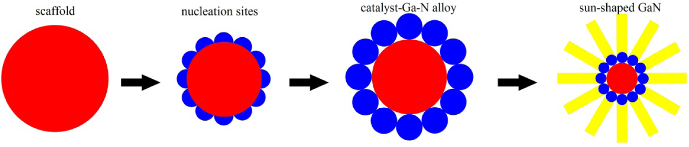
Schematic diagram of the possible growth mechanism of sun-shaped GaN nanowires: Fe-Cr metal complex acts as a scaffold; Ga and NH3 gases evaporate and dissolve in the catalyst nucleation sites; catalyst-Ga-N alloy liquid droplets; growth of GaN nanowires
Figure 6 shows a possible schematic to further illustrate the details of the VLS growth of GaN nanowires. At first, the Fe-Cr metal complex forms many large drops, which act as a scaffold, after which many nucleation sites appear on the surface of this scaffold at a proper temperature. Secondly, Ga and NH3 gases evaporate and dissolve in the catalyst nucleation sites to form catalyst-Ga-N alloy liquid droplets. Finally, when the concentration of GaN reaches saturation, these catalyst-Ga-N alloy liquid droplets can serve as nucleation sites, so that the GaN can begin to grow. In this process, we suggest the key point in forming sun-shaped GaN nanowires is the critical role played by the “scaffold”, which means that these nucleation sites are not dispersive but gather at the surface of the scaffold. Nonetheless, the important question about why the especially pure cubic GaN structure existed is still fascinating and we have presented a possible hypothesis based on many previous research results. We believe that the “stacking defects” play an important role during the growth of cubic GaN nanowires [26]; see the analysis in Figure 3. The stacking defects may change the growth energy of GaN and form a metastable cubic structure of GaN. However, further detailed investigations are necessary.
4. Conclusion
Straight and curved sun-shaped single crystalline GaN nanowires have been fabricated by controlling the gallium/nitrogen reactant ratio through the facile CVD method via a VLS process. For the straight nanowires, a straight and uniform diameter of about 20 nm with a high-quality hexagonal structure was displayed. However, the curved nanowires showed a surprisingly pure cubic structure with a diameter of 100 nm and a length of several hundred micrometres, with many stacking faults also observed in these curved nanowires. PL spectra studies revealed that both of these GaN nanowires indicated a strong UV emission band at 370 and 400 nm, respectively, which suggests a potential use in optoelectronic and electronic devices.