
Abstract
Bionic devices are implants that replace biological functions that have been lost due to damaged or lost tissue. The challenge of this area is to find the appropriate materials to match the biocompatible criteria with the same mechanical and electrical performance. In this research, a new method is introduced for the enhancement of silicon biocompatibility by fabrication of a 3D nanofibrous layer on the silicon surface, induced by nanosecond laser pulses at a high repetition rate and power. It was found that the laser treatment with smaller line spacing and a higher overlap number enhanced the biocompatibility of silicon. The results display a promising improvement in the biocompatibility of silicon for the production of biomedical devices such as sensors, bio-MEMS and nano-biomaterial fabrications.
Keywords
1. Introduction
Today's health sciences and technologies are mainly oriented around increasing quality of life. An important topic of study in this area is the development of new technologies capable of high interactions with various aspects of the human body, such as artificial organs and bionic devices. Recent improvements have extended the application of biomedical engineering to the successful evolution of highly sensitive organs, such as bioprosthetic total artificial hearts [1]. Despite the tremendous progress made in this field, there remains critical challenges in the biocompatibility and bioactivity of the materials used in bionic implanted devices; these materials include both organic and inorganic materials, such as gold, titanium, polymers, bioceramics and composites [2-6].
Nanoparticles of gold, as a completely biocompatible material, have been widely used in biosensing applications [7-9]; significant research is being conducted to allow the application of more affordable and easily accessible materials that fit the biocompatible criteria, while offering the same mechanical, electrical and chemical performances. A biomaterial frequently used for its semiconductor abilities is silicon [10-13]. Biomedical devices and micro-electromechanical systems for the biomedical field (Bio-MEMS) have been fabricated using this material [14, 15]. Silicon nanoparticles are heat-free and, when they are excited via a laser, they will not damage living biocells [16]. Other favourable properties of silicon include its nontoxicity and elasticity.
Silicon in its pure form is not biocompatible, but can be used for these biomedical devices if certain surface modifications are made to its surface [17, 18]. Any silicon-based bionic device requires a biocompatible packaging. A proposed method is to coat silicon in titanium, which is a biocompatible material. This has been done with a titanium-coated silicon implant, which results in a reduction of capsular inflammation when compared to a regular silicone implant for plastic surgery [19, 20]. A thin film of titanium can be deposited onto the surface via physical or chemical vapour deposition.
Another proposed method is to directly modify the surface of silicon by chemical etching using acid [21]. This will create a porous silicon layer that increases the specimen's capability of cell adhesion. Porous silicon is also used for other medical devices in drug delivery and cancer treatment [22-25]. Though chemical treatment is a popular approach used to modify silicon's surface, there are risks of complications with a multi-step chemical process that can prove to be inefficient or time consuming.
The most important objective of this research is to introduce a new method for the enhancement of silicon's biocompatibility by synthesis of a thin biocompatible layer of a 3D nanofibre structure (nanoporous) of silicon oxide on its untreated surface. This study focuses on laser treatment with Nd:YAG nanosecond laser pulses at a high repetition rate and power, which produces 3D nanofibrous structures on the surface of silicon. This technique uses an abundant and affordable material and pairs it with the simplest of laser techniques. The advantages of the laser system include the high controllability of parameters and a decrease in manufacturing time. The most effectual asset of this method is that it is a one-step process and that one-step process can be conducted under ambient conditions. The aim of this study is to help patients whose bodies have damaged or missing tissues. Biocompatible silicon has the potential to produce devices for replacing tissues, particularly in the eye, skin, ear or nasal cavity [21]. The silicon would be used as a scaffold where the cells will be cultured on its surface.
2. Materials and Methods
2.1 Laser processing and the generation of nanofibrous structures
The laser used in this experiment is a nanosecond Nd:YAG pulsed laser with a wavelength of 1064nm. A simple line pattern was made on silicon wafers with the orientation <100>. These patterns were made above the ablation threshold, at a submicro scale with the various line spacings of 0.15mm, 0.10mm, 0.05mm or 0.025mm. The laser would repeat the line pattern for one, two and three loops (or “overlaps”) for different samples. The scanning speed of the laser was set to 100mm/s. The power was an average of 13.8W and the frequency was kept constant at 100 kHz.
2.2 Sample soaking in SBF for in vitro assessment
Simulated body fluid (SBF) is a solution that mimics the ion concentration of human blood plasma. Two sets of samples were then submerged in SBF for the periods of two weeks and four weeks. The temperature of the incubator was kept constant at the average human body temperature of 36.5°C. The SBF was prepared according to the ingredients proposed by Kokubo and Takadama [26].
2.3 Surface characterization
2.3.1 Field Emission Scanning Electron Microscopy (FESEM) and Energy Dispersive Spectroscopy (EDS)
The samples were analysed using a Field Emission Scanning Electron Microscopy. The model used was the Hitachi SU-70 Field Emission Gun (FEG) SEM. The Schottky thermal emitter allowed for ultra-high resolution images of the samples, which were used to compare the different overlaps and line spacings. In order to verify the elements present on the samples after soaking them in SBF, the Energy Dispersive Spectrometer (EDS) was used. The EDS can determine the chemical composition of materials and is used within the FESEM apparatus.
2.3.2 Micro-Raman Spectroscopy
The Renishaw in Via micro-Raman spectrometer, equipped with 514.5 nm Ar-ion laser focused through a x50 objective lens (N. A. = 0.75), was used to further identify the chemical composition of the silicon samples, both before and after the use of SBF. The EDS results involved the individual elements of the surface, but not the chemical compounds, which were provided by the micro-Raman machine.
2.3.3 3D Optical Microscopy
This study used the Zeta-20 Optical Profiler to scan the surface of the samples in order to obtain the average surface roughness across each sample.
2.3.4 Light spectroscopy
In order to verify the optical properties of the treated silicon samples at different overlaps and line distances, the reflection spectrum was measured using the STS-NIR spectroradiometer (Ocean Optics, Dunedin, Florida, USA) with the optical resolution of 1.5 nm. The measurement was conducted for wavelengths in the range of 650–1100 nm.
2.4 Statistics
All experiments were carried out in Minitab® and the data points are averages unless otherwise mentioned. The error bars indicate standard deviations.
3. Results and Discussion
The first figure shows a series of photos taken of the untreated silicon with the FESEM before the samples were soaked in SBF. The first row, Figures 1(a) through 1(c), shows silicon with one overlap (OL) for the line spacings (a) 0.025mm, (b) 0.05mm and (c) 0.10mm. The second row, Figures 1(d) through 1(f), shows two overlaps for the same line spacings, and the third row, Figures 1(g) through 1(i), show the results for three overlaps.

FESEM images of silicon at different overlaps (a) 1 OL 0.025mm, (b) 1 OL 0.05mm, (c) 1 OL 0.10mm, (d) 2 OL 0.025mm, (e) 2 OL 0.05mm, (f) 2 OL 0.10mm, (g) 3 OL 0.025mm, (h) 3 OL 0.05mm, (i) 3 OL 0.10mm
As shown in Figure 1, both increasing the number of overlaps (scanning loops) and decreasing the laser-scanning line distances results in the formation of 3D nanofibrous structures on the treated surface of Si samples. Figure 2 shows a close-up FESEM micrograph image of the nanofibrous structure generated on the Si surface at the laser-scanning line distance of 0.025 mm for three loops. The nanofibres consisted of self-assembled bridges and closed rings in which nanoparticles of silicon oxide are bonded together. The average diameter of synthetic fibres is 57nm and, as previously stated by [27], they are made of silicon oxide.
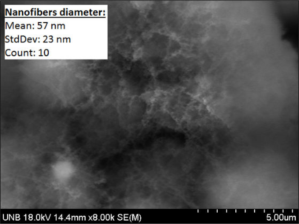
FESEM image of silicon nanofibres synthesized at: 3 OL, 0.025mm; average diameter: 57 nm
When the laser irradiates the surface, it creates a high-temperature reactive plume around the contact area and generates a shockwave. The laser ablation causes the silicon to oxidize within and around the plume. When the vapour reaches the outer wall of the plume, the SiO2 becomes supersaturated, allowing nucleation. Once the laser has passed and the pattern cools below the point of sublimation, the nanofibres being to aggregate on the surface [28, 29]. This nanoporous structure can be seen on the samples in Figure 2. Figure 3 illustrates the formation of the plume and particles.

Plume and nanoparticle formation of silicon during laser processing
It has been shown in the literature that these nanoporous structures can improve the bioactivity of the surface of silicon, as well as titanium. The porous areas increase their wettability when soaked in SBF, which results in hydroxylation of the silicon, producing an Si-OH layer. The SiO2 surface has a negative charge and leads to calcium phosphate nucleation, forming hydroxyapatite [5, 29, 30]. Figure 4 shows the same samples with the same orientation as that in Figure 1, but Figure 4 consists of FESEM images from the silicon samples that have been soaked in SBF for a period of four weeks.

FESEM images of silicon at different overlaps after soaking in SBF for four weeks: (a) 1OL 0.025mm,(b) 1OL 0.05mm, (c) 1OL 0.10mm, (d) 2OL 0.025mm, (e) 2OL 0.05mm, (f) 2OL 0.10mm, (g) 3OL 0.025mm, (h) 3OL 0.05mm, (i) 3OL 0.10mm
It can be seen in Figure 4 that as the overlaps increase in number, the more bone apatite is deposited on the surface. It can also be seen that for each of the overlaps, the most bone apatite is found on the smallest line spacing: 0.025mm. This is due to the fact that the roughness has increased as the number of lines on the surface area increases. The increased surface area due to the change in roughness enables a higher cell-attachment rate. Surface roughness can enhance the absorption of light, both by multiple reflections in microcavities and by variation in the angle of incidence. Laser-induced periodic surface structures may enhance absorption of laser energy via the generation of surface electromagnetic waves [31]. The initial pattern with one overlap increased the roughness, which allowed for more light absorption. By further increasing the overlap number to two and three, the contact surface increased, allowing more apatite to be deposited on the silicon.
To further prove that a higher number of overlaps yields the best outcome, the EDS results were taken for different overlaps at 0.025mm line spacings. These results are presented in Figure 5.

EDS results of four-week SBF samples for 0.025mm at (a) 1 OL, (b) 2 OL and (c) 3 OL
The EDS results show the increase in bone-like apatite elements such as calcium, chlorine, sodium and potassium. Greater quantities of these elements appear in Figure 5(c), and more apatite results at a higher number of overlaps. Figure 6 further proves these results with micro-Raman spectroscopy, looking at the SBF sample with a line spacing of 0.025mm at three overlaps.

Raman results for a 0.025mm line spacing at three overlaps with untreated silicon (Si) and after use of SBF (Si-HA)
The dotted line on the graph in Figure 6 shows the results before the samples were soaked in SBF. The solid line represents the results after soaking in SBF and peaks formed at a Raman shift of 600cm−1. This peak is characterized as potassium oxide (PO4), a bone-like apatite compound [32]. The 800cm−1 peak represents carbon and can be neglected due to the carbon coating required for the FESEM images. Both the EDS and Raman results illustrated in Figures 5 and 6 lead to the same conclusions and are, therefore, in close agreement.
As mentioned earlier, the roughness had increased with a higher number of overlaps and with a smaller line spacing. This is shown in Figure 7, where 3D microscopy was used to determine the surface roughness of the silicon samples. The roughness results obtained by 3D optical microscopy show the maximum roughness obtained for the laser-scanning line distance of 0.025 mm at three laser-scanning intersections (OL).

Surface roughness values for silicon for one, two and three overlaps at 0.025mm, 0.05mm, 0.10mm and 0.015mm line spacings, taken with a 3D optical microscopy
As shown in Figure 8, the reflection of the Si samples at near infrared (IR) wavelength decreases by increasing the number of overlaps (the loop number), as well as by reducing the line distance of the irradiated areas. This results in a larger volume of generated plasma plume and a higher nucleus density, as well as a higher number of evaporated silicon particles from the substrate, which leads to a higher deposition rate of generated nanofibrous (nanoporous) silicon oxide on the surface

Intensity of infrared for (a) increasing the loop number and (b) increasing the line distance
4. Conclusions
In this study, the effects of changing the number of overlaps and laser-scanning line distance on the biocompatibility of silicon were investigated. The results show that the apatite-inducing ability increases with a higher number of overlaps. Samples with a smaller line spacing of 0.025mm were also revealed to increase bone-like cell growth. With a higher surface roughness using nanofibres made with minor surface modifications, a silicon surface can become a biocompatible material.
The benefits that can result from using silicon for bionic devices fall into both the simplicity aspect and the affordability aspect of such usage. Silicon is the second most abundant element on earth after oxygen, and is consequently cost effective. When the processes involved with preparing the implant are simple and quick, time efficiency has a major effect of the availability of the final product. The biggest advantage of the treatment method used in this study is the controllability of the total process. In turn, this reduces the risks of any complications when implanting silicon into the human body. With this new research, silicon can potentially be used for the production of biomedical devices such as sensors, bio-MEMS and nano-biomaterial fabrications. In addition, this could involve the development of bionic devices for replacing damaged tissues in ears or eyes, which can receive any signal or optical information and convert them into biological signals.
Footnotes
5. Acknowledgements
This research is funded by the Natural Science and Engineering Research Council of Canada (NSERC), New Brunswick Innovation Foundation (NBIF) and the McCain Foundation.