
Abstract
This paper describes an easy and time-saving strategy for the fabrication of heterogeneous nanotubular arrays of TiO2-CdS (TCHNTAs) on transparent conductive glass (FTO) and their photoelectrochemical properties. The use of transparent FTO instead of opaque Ti substrate allows incident light from the substrate side. The anodized TiO2 nanotubular arrays were firstly detached from Ti substrate by anodization under a high voltage of 120 V and then transferred to FTO substrate using TiO2 (P25) paste as a binder, followed by sensitization with CdS nanoparticles. After optimizing the deposition cycles of CdS nanoparticles, the TCHNTAs on FTO substrate demonstrated an enhanced photocurrent density in the Na2S/Na2SO3 electrolyte under front-side illumination from the FTO side, which improved by ∼ 21% when compared with the photocurrent density under back-side illumination from the TiO2-CdS side. This improvement in photoelectrochemical properties can be ascribed to the reduced charge recombination on the interface between the TiO2 nanotubes and the CdS nanoparticles under front-side illumination. Our strategy for nanotubular transfer on transparent substrate may extend the applications of TiO2 nanotubular arrays into other fields, such as dye-sensitized solar cells, photochromism and photocatalysis.
1. Introduction
Since the discovery of the Fujishima-Honda effect in 1972, titanium dioxide (TiO2) has been used as a typical photoelectrode in water photoelectrolysis to convert solar energy for the production of H2.[1-3] Currently, anodized TiO2 nanotubular arrays are one of the most promising architectures, owing to their special features of facile fabrication, tunable structural parameters and high electron collection efficiency.[4-12] A critical drawback of TiO2 nanotubular arrays is their large band gap, which means that only the ultraviolet (UV) region of the solar spectrum can be utilized. Coupling TiO2 nanotubular arrays with a low-band-gap semiconductor of CdS nanoparticles to form heterogeneous nanotubular arrays of TiO2-CdS (TCHNTAs) has been adopted as a method to extend the photoelectrochemical activity from UV to visible light. [13-26] Traditionally, it is understood that TCHNTAs on the opaque Ti substrate can only be illuminated from the photoactive TiO2-CdS layer, which limits their photoelectrochemical activity.[13-22] Therefore, transfer of TCHNTAs onto transparent conductive glass (FTO) has great potential to improve their photoelectrochemical properties.[23-26] Bai et al. fabricated TCHNTAs on transparent substrate using anodized Ti film on FTO by sputtering. [23] Guan et al. fabricated TCHNTAs using self-standing TiO2 nanotubular arrays, which were formed by a low-voltage anodization (for 3–7 h) and H2O2 dissolution (for 2 h). [24] Liou et al. reported TCHNTAs using self-standing TiO2 nanotubular arrays formed by immersing anodized TiO2 nanotubes on Ti metal in H2O2. [25,26] However, these strategies were complex and time consuming, and offered low flexibility in regulation of tubular length. Development of an effective strategy to fabricate TCHNTAs on FTO substrate still remains a challenge.
In this paper, we describe an easy and time-saving strategy to fabricate TCHNTAs on transparent FTO substrate. The anodized TiO2 nanotubular arrays are detached from Ti substrate by anodization under a high voltage and then transferred to FTO substrate using TiO2 (P25) paste as a binder, followed by sensitization with CdS nanoparticles. Our results indicate that TCHNTAs on FTO substrate demonstrate an enhanced photocurrent density in the Na2S/Na2SO3 electrolyte under front-side (FS) illumination from the FTO side, which is improved by ∼ 21% when compared with the density under back-side (BS) illumination from the TiO2-CdS side.
2. Experiment
2.1. Fabrication of TiO2 nanotubular arrays on Ti foil
TiO2 nanotubular arrays were formed by a two-step electrochemical anodization. In the first step, Ti foil was anodized in ethylene glycol solution (Beijing Chemical Factory, China) containing 0.25 wt% ammonium fluoride (Beijing Chemical Factory, China) and 2 vol% Milli-Q water under a voltage of 60 V for 30 min. [27, 28] The voltage was applied using a DC power supply (HB17601SL2A, Shanghai Meitian Wiring Co., Ltd.). Pt foil of size 2×2 cm2 acted as a cathode. The anodized Ti foil was ultrasonically treated in 1 M HCl for 20 min to completely remove the TiO2 nanotubular arrays. In the second step, the textured Ti surface was anodized in the same electrolyte for 45∼180 min at a voltage of 60 V to form highly ordered TiO2 nanotubular arrays. After anodization, the sample was cleaned with isopropanol and dried in air, followed by annealing at 450°C for 3 h.
2.2. Transfer of TiO2 nanotubular arrays onto transparent conductive glass (FTO)
TiO2 nanotubular arrays were detached from the Ti foil by anodization under a high voltage of 120 V in the above-mentioned electrolyte for 3∼5 min (depending on tube layer thickness) under a temperature of 15°C. [29-33] The free-standing nanotubular arrays were cleaned in isopropanol repeatedly and then dried in air. Then, the crack-free membranes were heated at 100°C for 1 h in air.
A TiO2 paste was prepared by mixing TiO2 nanoparticles (P25, Degussa) with 3 vol% acetic acid solution (Beijing Chemical Factory, China) at the weight ratio of 1:20. [33] The paste was deposited on the surface of FTO substrate (fluorine-doped SnO2 sputtered on glass) using a doctor-blade technique. Consequently, the free-standing TiO2 nanotubular arrays were attached to TiO2-paste-coated FTO substrate, followed by calcination at 450°C for 3 h.
2.3 Deposition of CdS nanoparticles
CdS nanoparticles were deposited on TiO2 nanotubular arrays on FTO substrate with a successive ionic layer adsorption and reaction (SILAR) method. [14] Briefly, the as-prepared TiO2 nanotubular arrays on FTO substrate were immersed in a 0.05 M Cd(NO3)2 aqueous solution (Beijing Chemical Factory, China) for 40 s. After rinsing thoroughly with Milli-Q water, they were immersed in a 0.05 M Na2S solution (Beijing Chemical Factory, China) for another 40 s, followed by another thorough rinsing. The SILAR process was repeated until the desired amount of CdS nanoparticles was achieved. The obtained heterogeneous nanotubular arrays of TiO2-CdS were denoted as TCHNTAs.
2.4 Characterization
The morphology of the TCHNTAs was examined using a JEOL JSM-7500F field emission scanning electron microscope (FESEM) and an FEI Quanta FEG 250 environmental scanning electron microscope (SEM). The crystallization was characterized using a Shimadzu XRD-6000 X-ray diffraction (XRD) meter.
2.5 Photoelectrochemical measurements
The photoelectrochemical properties of the TCHNTAs on FTO substrate were characterized in a standard three-electrode cell with a quartz window using a CHI660D potentiostat (Shanghai Chenhua Apparatus Co., China). A Pt wire was used as a counter electrode and a saturated Ag/AgCl electrode acted as a reference electrode. The electrolyte was an aqueous solution of 0.35 M Na2SO3 (Beijing Chemical Factory, China) and 0.24 M Na2S (Beijing Chemical Factory, China). The light source was an Xe lamp (Beijing OPTPE Photoelectric Technology Co. Ltd., China) with an irradiance of 100 mW/cm2, which was calibrated by a standard Si solar cell (Beijing Perfectlight Technology Co. Ltd., China). The front-side (FS) illumination was defined such that the incident light came from the FTO side. Correspondingly, the back-side (BS) illumination was defined such that the incident light came from the TiO2-CdS side. Optical band-pass filters (Shenyang HB Optical Technology Co., Ltd., China) were used to measure the incident photon-to-electron conversion efficiency (IPCE). IPCE is defined as the ratio between the number of the photogenerated electrons (n) and the number of incident photons (N). If an electrode with 1 cm2 area generates a photocurrent density of I (A/cm2), the number of photogenerated electrons (n) per unit time is calculated by equation 1:

Flow chart for the fabrication of heterogeneous nanotubular arrays of TiO2-CdS (TCHNTAs) on transparent conductive glass (FTO)

Photographs of TiO2 nanotubular arrays on FTO substrate before (a) and after deposition of CdS nanoparticles for 30 (b) and 60 cycles (c)

Herein, e is the charge of one electron.
The number of incident photons irradiated on the electrode with 1 cm2 per unit time is calculated by equation 2:

Herein, P is the irradiance intensity of incident light; λ is the wavelength of incident monochromatic light; h is the Planck constant.
The IPCE is then calculated by the following equation 3:
3. Results and discussion
As shown in Scheme 1, the fabrication of heterogeneous nanotubular arrays of TiO2-CdS (TCHNTAs) on transparent conductive glass (FTO) involves four steps: (1) formation of TiO2 nanotubular arrays (anatase phase) on Ti foil by a two-step electrochemical anodization in fluoride-containing organic electrolyte; (2) detachment of TiO2 nanotubular arrays from Ti foil to form a self-standing membrane by anodization at a high voltage; [29-33] (3) immobilization of TiO2 nanotubular membrane on FTO substrate using TiO2 (P25) paste as a binder; [33] (4) deposition of CdS nanoparticles on TiO2 nanotubular arrays to form TCHNTAs by successive ionic layer adsorption and reaction (SILAR). The deposition of CdS nanoparticles changed the colour of the TiO2 nanotubular arrays from pale to darker yellow, and finally to orange (Scheme 2).
Figure 1 shows the typical top-view and cross-sectional SEM images of TiO2 nanotubular arrays before and after different cycles of CdS deposition. The cross-sectional image of TiO2 nanotubes (Fig. 1a) displays a uniform vertical alignment with an average internal diameter of ∼ 67.5 nm and a wall thickness of ∼ 15.1 nm, while the surface of the TiO2 nanotubes was covered by a porous TiO2 layer with pore diameter of ∼ 75.5 nm (as shown by top-view image in Fig. 1a). After several cycles of CdS deposition, the colour of the TiO2 nanotubular arrays changed from pale to darker yellow, and then to orange (Scheme 2), indicating that CdS nanoparticles were deposited on the surface. Figs. 1b, c and d indicate that after 10, 30 and 50 cycles of CdS deposition, CdS aggregates (formed by CdS nanoparticles) with a size of ∼ 22.4 nm could be observed more and more clearly, mainly distributed on the surface of the TiO2 nanotubes. From the cross-sectional image (Fig. 1c) after 30 cycles of CdS deposition, it can be seen that a small quantity of CdS nanoparticles was deposited on the inner surface.
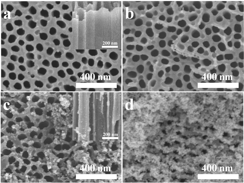
Top-viewed and cross-sectional SEM images of TiO2 nanotubular arrays on FTO substrate before (a) and after CdS deposition for 10 (b), 30 (c) and 50 (d) cycles
The crystallization of CdS nanoparticles was characterized using XRD measurements. Fig. 2A shows the XRD patterns of the FTO (fluorine-doped SnO2), TiO2-nanotube/FTO and TCHNTAs/FTO electrodes with CdS deposition of 50 cycles. The blank FTO substrate is shown in Fig. 2Aa; TiO2 nanotubular arrays on FTO were typically composed of anatase phases (Fig. 2Ab). After deposition of CdS nanoparticles, two diffraction peaks at 2θ= 26.5° and 44.0° appeared, which could be indexed to the (111) and (220) crystal faces of the cubic β-CdS phase (Fig. 2Ac). Fig. 2B shows that the broad diffraction peaks between 20° and 30° could be fitted as three diffraction peaks at 25.3°, 26.5° and 26.5°, identified as the diffraction peaks of SnO2 (on FTO), TiO2, and CdS, respectively. The wide XRD peaks at 26.5° of the cubic β-CdS phase were associated with the small size of CdS primary crystalline grains on the surface of the TiO2 nanotubular arrays.

(A) XRD patterns of FTO (a), TiO2-nanotube/FTO (b) and TCHNTAs/FTO (c) with CdS deposition of 50 cycles. (B),Fitting of the broad diffraction peak between 20° and 30°. The three fitting peaks were identified as the diffraction peaks of SnO2 (on FTO), TiO2, and CdS, respectively.
The formation of CdS nanoparticles was further evidenced by UV-visible absorption spectra. Fig. 3 depicts the UV-visible spectra of the TiO2/FTO electrode and the TCHNTAs/FTO electrodes with CdS deposition of 20 cycles and 60 cycles. The length of the TiO2 nanotubes was ∼ 12 μm. The spectra indicated that the blank TiO2/FTO electrode absorbed mainly UV light with wavelength smaller than 420 nm. However, after CdS deposition of 20 cycles, the absorption edge (λmax) of the TCHNTAs/FTO electrode shifted into the visible region at a wavelength of 535 nm. By increasing the cycles of CdS deposition to 60, the λmax was shifted to be 605 nm. The absorbance of the TCHNTAs/FTO increased significantly not only in the UV region, but also in the visible region, which was mainly due to the formation of the CdS nanoparticles.

UV-visible absorption spectra of TiO2 nanotubular arrays on FTO substrate with CdS deposition for 0 (a), 20 (b), and 60 (c) cycles
Fig. 4A shows the photocurrent density/potential (FV) curves of the TCHNTAs on FTO substrate with CdS deposition for 60 cycles under back-side (BS, from TiO2-CdS side) and front-side (FS, from FTO substrate) illumination, respectively. The length of the TiO2 nanotubes was ∼ 8 μm. The electrolyte was an aqueous solution of 0.35 M Na2SO3 and 0.24 M Na2S. The open-circuit photopotentials (OCP) under both BS and FS illumination were ∼ −1.2 V (vs. Ag/AgCl). It was clearly shown that the FS illumination generated a much higher photocurrent density than BS illumination in the potential interval between OCP and 0 V (vs. Ag/AgCl). At a typical potential of 0 V (vs. Ag/AgCl), the photocurrent density under FS illumination was 5.93 mA/cm2, which was improved by 21.3% compared with that under BS illumination (4.89 mA/cm2). CdS nanoparticles were proven to be an effective sensitizer for TiO2 nanomaterials, which could extend the photoelectrochemical responses of the electrode in the visible region. [34-38] The spectra of incident photon-to-electron conversion efficiency (IPCE) indicated that the TCHNTAs on FTO substrate under FS and BS illumination demonstrated strong photoelectrochemical activity in the visible region (Fig. 4B). It was clear that the IPCE under FS illumination was higher than that under BS illumination in the wavelength range between 430∼510 nm.

(A) Photocurrent density-potential curves of TCHNTAs on FTO under illumination from front side (FS, a) and back side (BS, b), and under darkness (c). The inset shows schematic diagrams of FS and BS illumination. (B) IPCE curves of TCHNTAs on FTO under FS (a) and BS (b) illumination. The length of TiO2 nanotubular arrays is ∼ 8 μm. The cycle of CdS deposition is 60.
We systematically studied the effect of CdS deposition cycles (i.e., the amount of CdS nanoparticles) on the photoelectrochemical properties of TCHNTAs on FTO under FS and BS illumination. As shown in Fig. 5, for both illumination directions, the increase in the deposition cycles of CdS improved the photocurrent density because of the increased amount of photogenerated electrons transferred from excited CdS nanoparticles under illumination. However, the relative magnitude of photocurrent density under FS and BS illumination showed a significant dependence on the deposition cycles of CdS nanoparticles. When CdS deposition was less than 30 cycles, TCHNTAs under BS illumination generated a larger photocurrent density than those under FS illumination at a typical potential of 0 V (vs. Ag/AgCl). Meanwhile, when CdS deposition was more than 30 cycles, the photocurrent density of TCHNTAs under FS illumination surpassed that under BS illumination at a potential of 0 V (vs. Ag/AgCl).
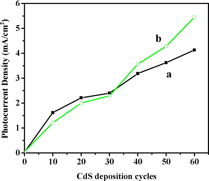
The effect of CdS deposition cycles on the photocurrent density of TCHNTAs on FTO substrate at 0 V potential (vs. Ag/AgCl) under BS (a) and FS illumination (b). The length of the TiO2 nanotubular arrays is ∼ 8 μm.
When CdS deposition was less than 30 cycles, the amount of CdS nanoparticles on the surface of the TiO2 nanotubular arrays was small, with the particles being tightly attached. When the TCHNTAs were illuminated from the TiO2-CdS side (back side), excited CdS nanoparticles could quickly release photogenerated electrons to the TiO2 nanotubes, and then to the FTO substrate. However, when TCHNTAs were illuminated from the FTO side (front side), the incident light could be absorbed and scattered by the FTO substrate and the TiO2 nanotubular layer, which reduced the irradiance intensity of incident light that could reach CdS layer, resulting in a reduced amount of photogenerated electrons collected by the FTO substrate. Therefore, when CdS deposition was less than 30 cycles, the TCHNTAs under BS illumination generated a larger photocurrent density that than those under FS illumination (Fig. 5).
Increasing the deposition of CdS nanoparticles to 60 cycles would increase the amount of CdS nanoparticles on the TiO2 nanotubular layer, improving the photocurrent density of TCHNTAs under both FS and BS illumination. However, FS illumination generated a much larger photocurrent density than BS illumination (Fig. 5). This phenomenon could be explained as follows. When the amount of CdS nanoparticles increased, the thickness of the CdS layer increased because the CdS nanoparticles were mainly distributed on the surface of the TiO2 nanotubes. The outer CdS nanoparticles could not come into direct contact with the surface. When the TCHNTAs were illuminated from the TiO2-CdS side, excited outer CdS nanoparticles were unable to quickly release photogenerated electrons to the TiO2 nanotubes, which then recombined with the photogenerated holes, resulting in low charge separation efficiency. Correspondingly, when the TCHNTAs were illuminated from the FTO side, although some incident light was absorbed and scattered by the FTO substrate and the TiO2 nanotubular layer, CdS nanoparticles attached on the surface of the TiO2 nanotubes would be excited first, which resulted in high charge separation efficiency and therefore a high photocurrent density.
4. Conclusions
In conclusion, this paper has reported an easy and time-saving means of fabrication of heterogeneous nanotubular arrays of CdS-TiO2 on transparent conductive substrate (FTO) by filling TiO2 nanotubular arrays with CdS nanoparticles via a successive ionic layer adsorption and reaction method. TiO2 nanotubular arrays were firstly detached from the Ti substrate by anodization under a high voltage and then transferred to FTO substrate using TiO2 (P25) paste as a binder. After optimizing the deposition cycles of the CdS nanoparticles, an enhanced photocurrent density was obtained in an Na2S/Na2SO3 electrolyte by front-side illumination from the FTO substrate, and compared to the results with back-side illumination from the TiO2-CdS side. The reduced charge recombination on the interface between TiO2 nanotubes and CdS nanoparticles under front-side illumination contributed to the improved photocurrent density. We believe that TiO2 nanotubular arrays on transparent conductive substrate might find other applications in the fields of dye-sensitized solar cells, photochromism and photocatalysis.
Footnotes
5. Acknowledgements
This work was supported by the National Natural Science Foundation of China (21571011), Beijing Natural Science Foundation (2133066), “Young Talents Plan” for the Universities in Beijing City, Fundamental Research Funds for the Central Universities (YWF-15-HHXY-019), Scientific Research Foundation for the Returned Overseas Chinese Scholars, State Education Ministry of China.