
Abstract
The last decade has seen an extensive development of the field of nanomaterials which are currently being used in their first commercial applications. This rapid development is necessarily connected with certain technological demands. This paper describes a technology for the manufacture of nanomaterials from solutions by electrostatic spinning or spraying. Although this method has been well known since the last century, there are still only a few high-quality devices that can be used for the research of new nanomaterials. The main reason for this is that the process of nanomaterials manufacturing is influenced by numerous processing parameters which need to be properly regulated, and furthermore all device components must be resistant to interference from high voltage. The technological requirements are thus stringent. Moreover, such a device must be multifunctional, compact and affordable. This paper describes the technical aspects of a unique laboratory device, i.e., device modules and central control, measured processing parameters, and their effect on the produced materials. The developed laboratory device meets the most demanding criteria for a nanotechnological laboratory device and helps facilitate and speed up the research and development of new nanomaterials produced in high electrostatic field.
1. Introduction
The method known as electrospinning (or electrospraying, which yields nano- or microparticles due to lower solution concentration) is well-known [1] and used in laboratory production of nanomaterials (most commonly synthetic and natural polymers, but also other inorganic materials), as well as for the theoretical study of electrohydrodynamic effects [2]. There is a multitude of various potential applications for materials produced by this method, the most important fields being, for example, media filtration, medicine, optics and electronics, among others [3, 4]. The wide use of this method has been facilitated by low purchase costs and the possibility of scale-up [5]. Its basic operation and nanomaterial production requires only a high-voltage power source (between approximately 50 and 500 kV/m) and two electrodes connected to opposite potentials. One of the electrodes (emitter or jet) feeds a polymer solution and shapes it into curved shapes with low curvature radius [6]. The forces of a high-voltage electric field create the so-called Taylor cone [7] and cause a fibre to form. The fibre is pulled by electrostatic forces towards the other, oppositely charged electrode (collector) which serves to collect the flying fibres [8]. During the flight of the fibre, an extremely fast evaporation of the solvent and solidification of the material occur. The whole movement of the fibre between the two electrodes is highly complicated and follows a completely random trajectory [9]. This chaotic movement causes the flying fibre to be deposited randomly on the opposite electrode, where it forms a fibrous material with fibre diameters ranging from 10 nanometres to tens of micrometres. This nanomaterial manufacturing process is affected by many parameters which can be divided into four categories: solution properties, processing parameters, electrode geometry and environmental conditions.
High-quality and repeatable production of nanomaterials with identical properties necessitates the regulation of processing parameters and environmental conditions according to the chosen settings. Moreover, all device electronics must be protected from interference from high-voltage wiring and extensive electromagnetic interference. This entails a significant increase in technological and design requirements for the device [10]. Here we report the development of a brand new device design with a transparent cylindrical deposition chamber and a control panel. The shape of the deposition chamber has been designed for optimal formation of the desired electrostatic field, user-friendly observation of the process, easy accessory installation, and easy access and cleanability of the interior. The materials used have the necessary chemical resistance to solvent systems applied in solution preparation. Central control with a distributed network of peripherals has been chosen specially for this device to meet the requirements concerning control quality, repeatability and operational safety. The user interface features a touchscreen with graphical environment designed to simplify and improve the efficiency of operation and to automate the production process automation. Several safety elements have been integrated into the device to ensure user safety and minimize the risk of injury by electric current from low- and high-voltage wiring.
2. Materials and methods
The device has been designed as a table-top device with outer dimension of 1090 × 980 × 660 mm, see Figure 1. The cylindrical chamber dimensions are (Ø660 × 650) mm. The device frame is plastic; parts of the interior walls are made of sheet metal. In order to operate, the device requires a power supply voltage of AC 230 V and a supply of compressed air of 3.5 ± 0.5 bar. The input power of the device in operation is lower than 150 W, reaching peak values of up to 600 W. The deposition chamber may be accessed via sliding cylindrical door (secured with a safety lock); electrodes (emitters and collectors) and syringes with a solution can then be attached on the inside.

A ballooned diagram of the device and its parts. (1) Exhaust aperture, (2) Collector bracket, (3) Spinning chamber, (4) Sliding door, (5) Emitter and air connector, (6) Dispenser, (7) Fuse box door, (8) Fuse board and instrumentation inside the machine, (9) Touchscreen, (10) Multifunction control, (11) Standby signal, (12) On signal, (13) Emergency stop button, (14) Compressed air, (15) Power (16) Safety clip, (17) Peripheral Ethernet connection, (18) Power button.
The inside of the chamber is illuminated with LED lights which provide sufficient illumination of the deposition chamber and make the process of the formation of a nanofibrous material clearly visible. The device is fully controlled with a touchscreen and a multifunctional knob, both located on the control panel. A block diagram of the central system is shown in Figure 2. The system can be divided into groups of modules for emitters, collectors, internal sensors, control elements and safety features.
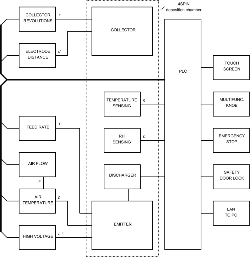
A block diagram of the central control system with a PLC
2.1 Emitter modules
The emitter modules provide all the functions of the emitter electrode, which are as follows: transmitting strong electrostatic voltage, solution dosing, supplying heated air and discharging residual charge from the electrode. The high-voltage source module (SMS60P60, Spellman) is regulated at 0 to 60 kV directly by the programmable logic controller (PLC; BMX Modicon, Schneider Electric) via an analogue signal of 0 to 10 V and resolution of 15 bits. The values of the incoming voltage and of the electric current flowing through the high-voltage branch are directly measured at the output of the high-voltage source (also an analogue signal of 0 to 10 V). There is a universal connector in the lower part of the deposition chamber compatible with all emitter types. The high-voltage source outlets are connected to a three-way connector, the third connection of which is connected to a ground clamp whenever the manufacturing process is not running. When the process is finished, a pneumatic drive connects the contacts, connecting both the emitter and the high-voltage power source outlet to zero potential. The operator can then safely handle the electrodes. In order to minimize waste during solution distribution, the container (a syringe of a volume of 10, 20 or 30 ml) has been integrated directly into the deposition chamber. Solution dosing from the syringe is controlled by a precise translation stage. A step drive (SX series, Microcon) moves the piston at a minimum speed of 1 μm/s. The drive and the container with the solution are mechanically connected to the plastic piston. The piston insulates sensitive electronic translation elements from high voltage which spreads from the emitter through the dosed solution.
2.2 Electroblowing
Controlling environmental conditions with an air-conditioning unit regulating humidity and temperature would significantly increase the total costs of the developed device. For this reason, an alternative solution has been designed which can influence the atmosphere around the emitter. Dry, filtered air from an external source is fed to the space closely surrounding the metal electrode of the emitter. The flow of the air is regulated with a flow meter with a proportional directional control valve (SFAB and MPYE, Festo) and kept at 3–100 lit/min. The temperature of the incoming air can be set independently of the flow to up to 100 °C. The air is heated with a heating unit (AHP series, Omega) connected to a power source of 230 V via a thyristor switch (Solitron Midi, Gavazzi). A thermocouple measuring the temperature of the flowing air is connected next to the heating unit. Each module is controlled by a special predictive PID algorithm developed specifically for this device. The algorithm allows the tangent forces influencing the produced Taylor cone to be set in the vicinity of the emitter. It also enables humidity to be reduced and the surrounding temperature to be adjusted throughout the space where nanofibrous material is formed. The ability to set these processing parameters has proven to be highly advantageous for three reasons: it allows even hard-to-spin materials to be processed using this method, the morphology of the material formed to be influenced, and production to be increased (all these advantages are demonstrated with examples below).
2.3 Collector modules
Collectors are grounded electrodes, either static or rotating. After attaching any collector, its contact is connected to the ground with a contact resistance of less than 0.3 Ω. Moreover, rotating collectors must be mechanically connected to the drive (Minimotor SA, Faulhaber). Depending on the type, rotating collectors can rotate at speeds of up to 5000 rpm and thus must be perfectly balanced. The distance of the collector from the lower emitter electrode is adjusted by vertically repositioning the whole collector (using Minimotor SA, Faulhaber). The distance can be adjusted between 50 and 250 mm. For this purpose, all collectors have been sized in such way that their lower plane is always at the same height and the emitters have been designed to be uniformly high.
2.4 Internal sensor modules
The modules of the internal sensors consist of heat sensors and relative humidity sensors. The detector itself (PTSV 120, Sensit) is located on the top part of the deposition chamber. The values of these processing parameters are informative and cannot be regulated by the device itself.
2.5 Control modules and safety features
The device is operated via a 10.4” touchscreen (HMI Magelis XBTGT, Schneider Electric) with control features for device and processing parameters setting, process controls, maintenance controls, user reports, saved procedure reports and regulating constant setting controls. The development of this unique interface was based on extensive experience with laboratory application of the electrostatic spinning method. Its main features have been designed in such way as to, among other things, ensure intuitive and simple operation, process automation and operational safety. After entering basic data (the types of the connected emitter and collector, their distance, etc.), the operator sets up the processing parameters (initial value of high voltage, collector revolutions, dosing speed, etc.) and activates the process. The device automatically initializes air heating, collector rotation and other subprocesses, and after reaching the values that have been set for the process, the operator activates high voltage. At that moment, solution dosing is automatically initiated. During the device's operation, the operator may select a parameter to be adjusted on the touchscreen. The set value can then be adjusted with a control knob while the operator observes the resulting changes in the process (the operator does not need to keep watching the display). When the set processing time elapses or the operator terminates the process, the subprocesses are automatically deactivated in order to reverse their activating order, residual charges are discharged and the deposition chamber door is unlocked.
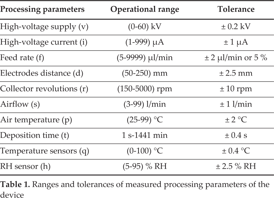
Processing data can be recorded and displayed with an external PC. Focusing on the data collection and recording speed, we have developed a mini SCADA system using the Modbus protocol. In test runs (with simulated data generation), the system reaches a recording speed of more than 3000 samples per second (kSPS = kilo samples per second) including their display in graphs. When the data are gathered in a real environment, the process is affected by connection latency and the speed of request processing by a remote system. With the central control (PLC) in place the speed is limited to 100 SPS. This value qualifies the system as a real-time monitoring system. To ensure maximum degree of experimental freedom in the preparation of new nanomaterials, the processing parameters can be set in wide ranges; the control system then regulates the parameters with deviations given in Table 1.
Ranges and tolerances of measured processing parameters of the device
2.6 Device accessories – emitters
Various accessories, mainly emitters and collectors, have been developed together with the device itself. The emitter system has been designed in such a way that the individual electrodes correspond to the individual stages of the production of a new nanomaterial. Usually, the initial necessary step is to convert the selected material into a nanostructure. An emitter with a single capillary jet is applied due to its exceptional ability to form the Taylor cone and accelerate the solution towards the collector (due to massive electric field gradient and the formation of a solution droplet with low curvature radius). After the solution has been successfully spun into a defectless nanomaterial with the desired properties, the process continues in the next development stages which focus on the production at higher throughput. Emitters with more capillary jets and other jetless systems are applied in these stages. By gradually increasing the production and simultaneously optimizing solution parameters, the fastest possible production of nanomaterials attainable with this method can be achieved. All the designed emitters are installed in the device with a universal quick coupler that ensures mechanical stability, connection with high-voltage source and hot air supply.
2.7 Device accessories – collectors
The system of basic collector types has been designed to meet the needs for the formation of nanomaterials of various macroscopic and microscopic parameters. A static plate collector or a rotating cylinder regulated at low revolutions are used for the production of larger layers with a random internal structure. The description of the principle of the electrostatic spinning method given above makes it evident that the fibres are deposited on the collector completely randomly. Single-axis arrangement of the fibres is obtained with a static or a rotating patterned collector [13] or with a cylindrical collector revolving at high speed. Depending on the intended application, by choosing from these collectors it is possible to produce either materials of large area with maximum dimensions of (36 × 25) cm2 and a random internal structure or smaller area layers with a high-quality regular internal structure. The designed collectors are attached to a special arm which provides mechanical stability to the attachment, vertical translation, grounding contact and mechanical connection with the rotating drive. This ensures a high degree of experimental freedom in the development of new nanomaterials and facilitates the installation of additional, newly developed collectors.
3. Results and discussion
The developed device was first tested for its ability to operate according to certain specified processing parameters and to produce these parameters within set tolerance limits. A set of production tests followed, focusing on the quality and repeatability of the produced nanomaterials at various device settings. The last testing phase was centred on the ability of the device to spin natural hard-to-spin polymers and synthetic polymers routinely processed with this method.
3.1 Processing parameters of the device
The data from the regulated processing parameters were recorded directly during the spinning process. A recording of voltage and current in the high-voltage branch is shown in Figure 3.

A recording of the changes in voltage and electric current between an emitter and a collector. The peaks in the current at the beginning of the process are caused by the formation of the Taylor cones.
The recording clearly shows initial peaks in electric current as the process initiates. Voltage is constant during the process. A time recording of airflow speed and air temperature in the vicinity of the emitters is shown in Figure 4. The temperature is sufficiently stable. The airflow recording shows a steep increase at the end of the process which is set automatically and helps speed up cooling of the internal parts of the device. Figure 5 shows the development of temperature and relative humidity in the whole deposition chamber. It is apparent that at the beginning of the process there was a decrease in humidity in the deposition chamber due to the incoming hot air.

A recording of air temperatures and flow speeds during the application of the electroblowing method. The examples also show an automatic increase in airflow speed after the conclusion of the spinning process that speeds up cooling of the internal components of the device.
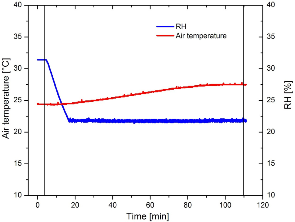
A recording of air temperature and humidity inside the deposition chamber. The decrease in humidity is caused by the incoming dry air during the application of the electroblowing method.
3.2 Production device tests
A 6 % solution of hyaluronic acid and polyethylene oxide (in a ratio of 80:20) dissolved in distilled water was used. A total of 10 samples with an exposition time of 10 minutes were prepared at identical device settings. An analysis of electron microscope images (Ultra Plus, Zeiss) yielded the values of average fibre diameters which are indicated in a graph in Figure 6. The average fibre diameter was (154 ± 58) nm (the uncertainty of the result is due to image analysis method error). Further samples were prepared at deposition times of 5, 10, 20 and 40 minutes. The resultant nanomaterial samples were weighted on an analytical balance (XS204, Mettler Toledo) and the measured weights are shown in a graph in Figure 7.

Measured average fibre diameters formed by repeated spinning of the same solution at identical processing parameter settings
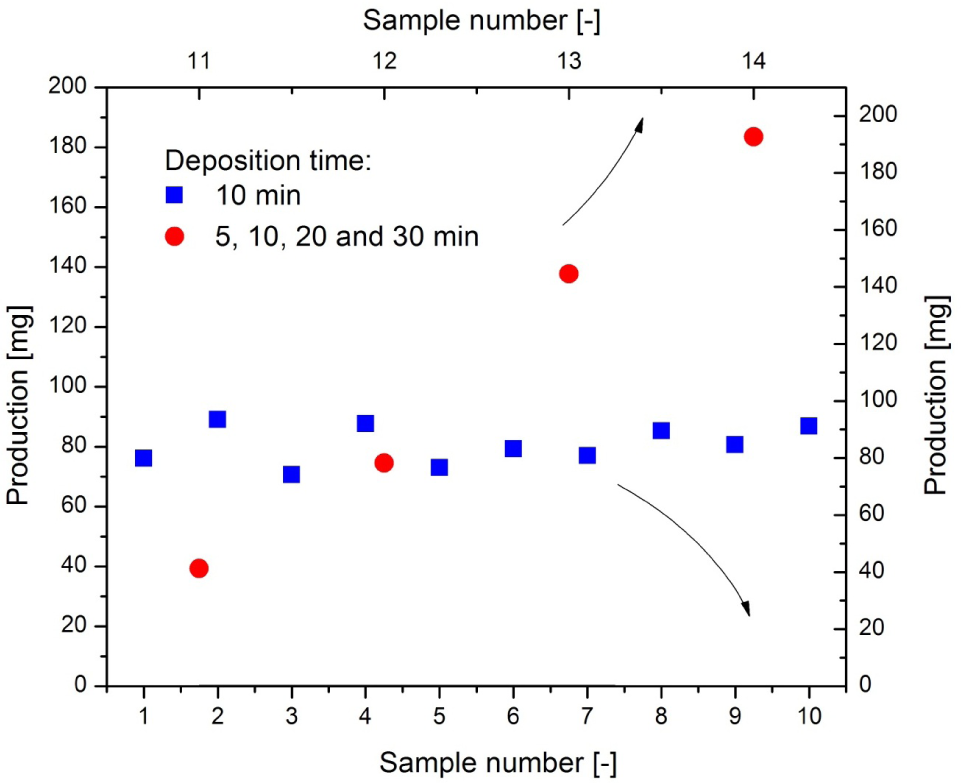
The weights of the produced nanofibrous layers formed by repeated spinning. Samples 1 to 10 were prepared at deposition time of 10 minutes and samples 11 to 14 at deposition times of 5, 10, 20 and 40 minutes, respectively.
The results indicate that a repeated production of a nanomaterial from an identical solution yield a material consisting of fibres of approximately the same diameters (see Figure 6) and weight (see Figure 7). The production speed was identical in all the repeat runs (81 ± 7) mg over 10 minutes of deposition (samples 1 to 10, see Figure 7); this production speed is directly proportional to the deposition time (samples 11 to 14, see Figure 7).
3.3 Produced nanomaterials
Approximately 20 different materials have been processed on the device so far; this paper presents only on overview of demonstrative examples in Table 2. Most of the materials were converted from their solutions into a solid form with a nanostructure without much difficulty; however, in all instances the process required optimization of solution parameters (especially concentration) as well as optimization of processing parameters. For example, hyaluronic acid in its native form (a 1 % solution in a mixture of water and acetic acid mixed in a ratio of 1:1) when spun at standard settings formed fibres with numerous structural defects caused by insufficient solvent evaporation. The electroblowing method had to be applied, helping to decrease the viscosity of the solution and speed up solvent evaporation.
An overview of spun materials. The average fibre diameter values are indicated for the given microscope images.

4. Conclusions
This paper describes in detail all parts of the device and its individual modules. The processing of materials into the form of nanofibres of desired qualities is facilitated by the device's wide array of reliable experimental functions. The developed laboratory device is controlled centrally by a PLC with programmed automatic and safety functions. Operating methods and technological capabilities are summarized by the process parameters and their tolerances achieved, which are supported by the results obtained within the data process record. These are the main advantages that distinguish our device from other devices on the market. It has been shown that accurate and stable control of process parameters contributes to the repeatability of new nanomaterial production. The functional capabilities of the device contributed to the research and development of new nanomaterials.
Footnotes
5. Acknowledgements
This research is partly conducted under financial support provided by the Technology Agency of the Czech Republic (project TA02011238: Novel wound dressings based on nanofibers and staple microfibers of hyaluronan and chitin/chitosan-glucan complex).