
Abstract
We report a thermal sensor composed of two multiwalled carbon nano-tubes (MWCNTs) inside a field-emission-scanning electron microscope. The sensor was assembled using a nanorobotic manipulation system, which was used to construct a probe tip in order to detect the local environment of a single cell. An atomic force microscopy (AFM) cantilever was used as a substrate; the cantilever was composed of Si3N4 and both sides were covered with a gold layer. MWCNTs were individually assembled on both sides of the AFM cantilever by employing nanorobotic manipulation. Another AFM cantilever was subsequently used as an end effector to manipulate the MWCNTs to touch each other. Electron-beam-induced deposition (EBID) was then used to bond the two MWCNTs. The MWCNT probe thermal sensor was evaluated inside a thermostated container in the temperature range from 25°C to 60°C. The experimental results show the positive characteristics of the temperature coefficient of resistance (TCR).
1. Introduction
Nanomechanical and nanoelectromechanical devices have been widely investigated in recent years. Our nanorobotic manipulation system has keys feature of nanometre-scale resolution and multiple-positioning degrees of freedom (DOFs) in real time. The nano-manipulator has been installed inside both a field-emission-scanning electron microscope [1] and a transmission electron microscope [2] to enable the assembly of nano-devices and the characterization of the properties of nano-blocks. Precise and controllable nano-fabrication methods are important to develop the novel type of nano-devices. One-dimensional nano-structures such as nano-wires and nano-tubes are basic building blocks for NEMS.
Since the discovery of multiwalled carbon nano-tubes (MWCNTs) [3], numerous applications of these materials have been developed, such as mass sensors [4], nano-radios [5] and nano-motors [6]. Nano-wires are solid one-dimensional nano-structures that include metallic nano-wires [7], semiconductive nano-wires [8] and non-metal nano-wires [9]; these nano-wires have applications as nano-needles [10], nano-hotwires [11], transistors [12], and nano-generators [13]. One challenge is to assemble and use a nano-sensor to detect the local environment of a single cell. The single cell is the basic element of life and represents the conjunction of energy and information. A nano-device is needed to measure and manipulate single cells because of their small size. A thermometer measures temperature or temperature gradient using a variety of mechanical, thermojunctive, thermoresistive, and radiative principles (infrared and optical pyrometers). When MWCNTs are used as a sensor, their extremely small size enables accurate temperature measurements at the nano-scale and reduces the possibility of disturbing the local environment. In addition, the small sensor size implies very low power consumption. To be used as a temperature sensor, a MWCNT-based thermal sensor should have the smallest possible time constant and provide an extremely rapid time response to the measured object's temperature. Fung et al. have reported the fabrication of an MWCNT-based thermal sensor. The bundled MWCNTs were assembled between two Au electrodes on a substrate [14]. Kuo et al. laterally grew MWCNTs between two electrodes to fabricate a thermal sensor. The MWCNTs were grown on the substrate between the electrodes [15]. Arai et al. reported a single-MWCNT thermal sensor with an MWCNT assembled on four electrodes [16]. The aforementioned sensors have the advantages of small size and low energy costs and are suitable for temperature measurements within the 2D surface of specimens. Because of the restrictions of their architectural design, these sensors can only be used to measure the temperature of specimens larger than 1 mm.
We here propose the fabrication of a thermal sensor composed of two MWCNTs inside a field-emission-scanning electron microscope. The advantage of such an MWCNT probe sensor is the ability to detect the local environment of a single cell with high accuracy, as shown in Fig. 1. The basic idea is to detect temperatures on the basis of the coefficient of resistance. Biological cells commonly live and are cultured at temperatures from 35°C to 37°C. When their temperature exceeds 43°C, most cells will be exterminated. We aimed to evaluate the performance of the thermal sensor in the range from 30°C to 60°C, as shown in Fig. 1.

The concept of a dual-CNT-probe thermal sensor
2. Nanorobotic manipulation system inside a field-emission-scanning electron microscope
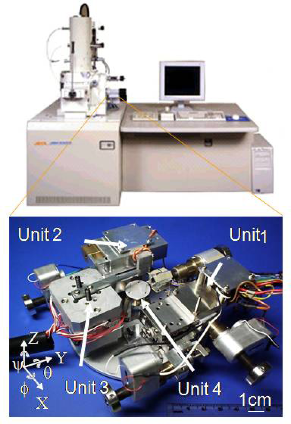
A nano-laboratory based on a nanorobotic manipulation system is presented in Fig. 2, and its specifications are listed in Table 1. The nano-laboratory consists of a nanorobotic manipulation system with a nano-instrumentation system and a nanofabrication system. It can be used to manipulate nano-materials – primarily but not limited to MWCNTs – to fabricate nano-building-blocks, assemble nanodevices, and analyse the properties of such materials, building blocks, and devices in situ. As a fundamental technique for the nano-laboratory, nanorobotic manipulation has opened a new path to construct nano-systems in 3D space, and will substantially broaden the possibilities for nano-analysis and nano-fabrication.
Specifications of the nano-laboratory
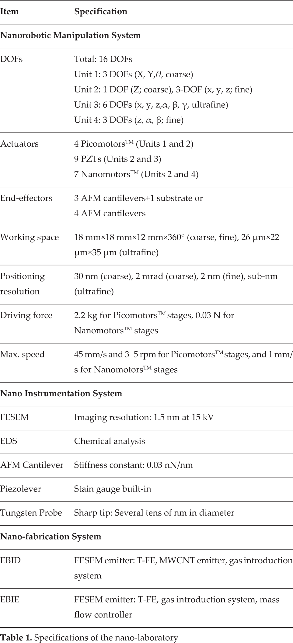
The nanorobotic manipulation system inside a field-emission-scanning electron microscope
A simplified conventional gas supply system was constructed for the electron-beam-induced deposition (EBID) system. The gas supply system can directly provide the precursor vapour and does not require that the precursor be heated because both of the precursors used in this work have low sublimation temperatures; the precursors can therefore be vaporized at room temperature through the opening of the glass tube to participate in reactions under the electron beam. A simplified precursor gas injection system (GIS) was constructed. A graduated pipette tip was used to deliver the precursor to the sample inside the field-emission-scanning electron microscope. The precursor powder was placed inside the pipette tip (the tip inner diameter was 400 μm), and the end of the pipette tip was sealed with tape. The precursor powder sublimed to form a gas inside the vacuum chamber. The GIS was positioned several cm from the sample [17]. In our study, EBID was investigated using organometallic compounds, including tungsten hexacarbonyl (W(CO)6).
The following kinematics derivation of the nano-manipulator is based on the Denavit–Hartenberg (D–H) notation. Modelling of the Unit-1 nano-manipulator is shown in Fig. 3. As evident from the link frame assignments in Fig. 3, frame 0 and frame 1 are coincident. Frame 1 has a translational movement in the |Z0| axis away from frame 0. Frames 2, 3, and 4 will be moved relative to the movement of frame 1. Frame 2 has a translational movement in the |Y0| axis, and its movement will drag frames 3 and 4 together without affecting frame 1. Frame 3 has a translational movement in |X0| and only drags frame 4 during its movement, without affecting the position or orientation of frames 1 and 2. Frame 4 is a tool frame.
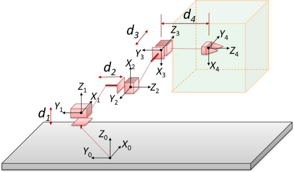
Kinematic parameters and frame assignments for nano-manipulator Unit 1
Frame i has an offset to frame (i − 1), which is described by three dimensions Xi−1,iii, Yi−1,i,iiZi−1,iii along Xi−1i, Yi−1i, Zi−1i, respectively. These values are constant and are based on the dimensions of the manipulator. The cubic region indicates the working space of the nano-manipulator.
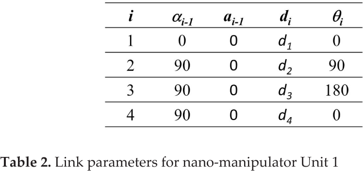
The link parameters of nano-manipulator Unit 1 are shown in Table 2, where i denotes the code number of the joints, ai−1 i is the link length, ai−1 i is the link twist, dii is the distance between links, and θii is the angle between links. The offset parameter of each frame is not listed in Table 2. To overcome this issue, we intentionally added the offset parameters to the transformational matrix. Because of this slight modification, we are able to include all of the dimensions, including the variable and constant values, in the kinematics derivation of Unit 1.
Link parameters for nano-manipulator Unit 1
By defining new symbols for sin and cos as s and c, respectively, we can represent the homogeneous transformations for each link as follows:

Finally, the product of all four link transformations is:

where d is the sliding transformation of each motor and X, Y, and Z are the constant values related to the nano-manipulator's structure.
3. Design and assembly of the nano-probe thermal sensor
A nano-wire probe was designed by the temperature coefficient of resistance (TCR) method. The electrical resistance of a conductor depends upon collisional processes within the wire. The resistance is expected to increase with temperature because the number and frequency of collisions increase. An intuitive approach to temperature dependence leads one to expect a fractional change in resistance that is proportional to the temperature change. Other researchers have previously used bundled MWCNTs or a single MWCNT assembled on a substrate. As current flows through the MWCNTs, the phenomenon of remote joule heating will directly heat the substrate. To decrease the interference from the local substrate, we designed a probe-type MWCNT thermal sensor. Dual MWCNTs were attached to a cantilever probe. This design not only decreases the local heating interference, but can also potentially be used for single-cell analysis.
On the basis of the temperature coefficient of resistance, we designed a probe-type thermal sensor using MWCNTs. The basic design is based on the change in resistance of MWCNTs in response to a temperature change. An atomic force microscopy (AFM) cantilever was used as a substrate; the cantilever was constructed of Si3N4 and coated with an Au layer on both sides. MWCNTs were assembled on the surfaces of the ATM cantilever; another cantilever was then used to force the MWCNTs to touch each other.
In the assembly, an AFM cantilever (Olympus, OMCT-TR400PB-1) was used as an end-effector to pick-up the MWCNT. The AFM cantilever was constructed of Si3N4 and was coated with a layer of Au on both sides. We used the AFM cantilever as a robot hand to pick up and assemble the MWCNTs. The MWCNT probe was fabricated from its bulk, which was synthesized by the arc-discharge method. First, an AFM cantilever was manipulated to pick up an MWCNT from the MWCNT bulk. The top surface of the cantilever was used to pick up MWCNT 1. The cantilever was positioned below the MWCNT and then raised to use the Au surface to touch and bond to the MWCNT via Van der Waals forces. EBID points were used to reinforce the bonding between MWCNT 1 and the Au substrate, as shown in Fig. 4(a). In the second step, we turned the cantilever over and attached MWCNT 2 to the back surface of the Au surface, as shown in Fig. 4(b). In the third step, we used another cantilever to manipulate MWCNT 1 to touch MWCNT 2, as shown in Fig. 4(c). Then, an EBID point was deposited onto the MWCNT contact point to improve the bonding, as shown in Fig. 4(d). In total, four MWCNT-probe thermal sensors were fabricated. Defects in MWCNTs are problematic with respect to mechanical and electrical applications. Annealing can solve this problem. We applied a sweep voltage of −1 V to 1 V to anneal the MWCNTs. Fig. 5 shows the I–V curve of the annealing process. The results show that the electrical annealing process totally fixed the defects in the MWCNTs and resulted in a linear I–V curve. Because the electrical annealing requires little time at pressures less that 10−4 Pa, the resistance of the MWCNT-probe thermal sensor was the same as that before annealing.

Assembly of an MWCNT-probe thermal sensor using a nanorobotic manipulator: (a) pick-up of MWCNT1; (b) pick-up of MWCNT 2; (c) two-manipulator cooperation to bring dual MWCNTs into contact and bond them in place; (d) reinforcement of the MWCNTs' bonding via EBID
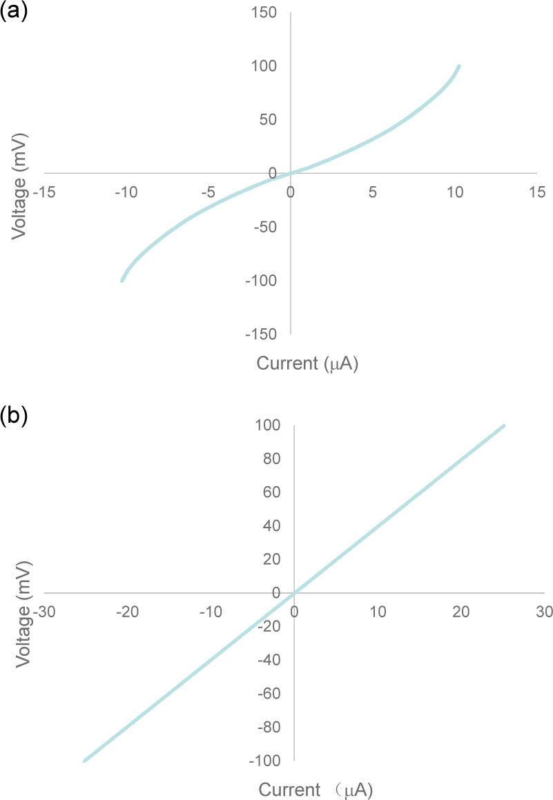
I–V curves demonstrating the effects of annealing of the MWCNTs
4. Results and discussion
Fig. 6 shows a schematic of the thermal-sensor experiment. A probe thermal sensor was positioned near the holder, which is shown in yellow in the Fig. 6. The two sides of the AFM cantilever were individually connected to positive and negative electrodes. The probe sensor was placed in an oven, and I–V curves were recorded at temperatures from for 30°C to 60°C at intervals of 5°C.

Schematic of the MWCNT-probe thermal sensor test setup
The oven was set to 30°C and was maintained at this temperature for 2 h. We then measured the I–V response of the MWCNT-probe thermal sensor. The resistance was 3960 Ω, with a standard error of 1.5 Ω. In the next step, we increased the oven temperature by 5°C to 35°C over a period of 1 h and maintained this temperature for 2 h. The resistance was 3970 Ω, with a standard error of 7.4 Ω. After this step, we measured the I–V response from 40°C to 60°C in steps of 5°C. The resistance values at 40, 45, 50, 55, and 60°C were 3980,3990,4000,4010, and 4030 Ω, with standard errors of 1.0, 1.9, 1.3, 11.1,and 1.0 Ω, respectively.
The experimental results in Fig. 7 show that the temperature coefficient of resistance of the MWCNTs is linear. The relationship is temperature=resistance −3891.8/2.2, and the standard error is in the order of 10 Ω. Metallic MWCNTs usually exhibit a resistance of several kΩ. Here, the temperature was increased in increments of 5°C because of the oven's limitations. The temperature coefficient of resistance was calculated as 0.05%.
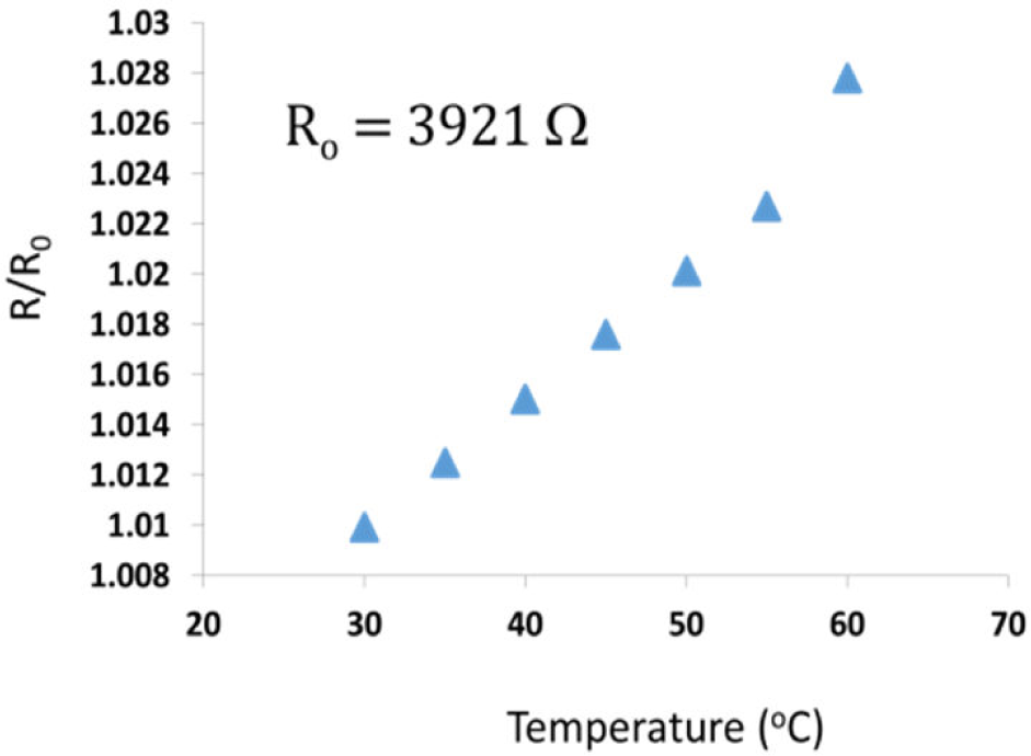
Evaluation of the MWCNT thermal sensor: R/R0 and temperature linear relation results
The total resistance of the nanothermal sensor Rtotal is given by

where Rc1 is the contact resistance of MWCNT 1 and its Au substrate, Rc2 is the contact resistance of MWCNT 2 and its Au substrate, Rc3 is the contact resistance between the two MWCNTs. The resistance of a carbon nanotube (CNT), RCNT, can be calculated by the following equation:

where ρCNT is the resistivity of the CNT, L is the length of the CNT, and d is the diameter of the CNT. In this work, CNT 1 is approximately 3 μm in length and 37 nm in diameter and CNT 2 is approximately 3 μm in length and 42 nm in diameter. The ρCNT is 3.5×10⁻⁵ Ω cm [18]. According to equation (7), RCNT = 1.8 kΩ.
Lan et al. discussed the metal carbon contact resistance and resistance of CNTs [19]. They reported that the resistivity of a MWCNT is 0.33 kΩ/μm and that the specific contact resistance of a CNT and Au surface is 4.4 kΩ/μm.


Therefore,
The calculated CNT resistances agree with the reference data and the theoretical calculations. The MWCNT can be considered as a graphene cylinder. Single-crystalline graphite exhibits a linear thermal response at temperatures greater than 200 K. [20] The evaluation result for our nanothermal sensor is also linear.
5. Conclusion
In summary, nanorobotic manipulation is a promising technique for the assembly of nano-sensors. With nanometre-lever resolution and real-time manipulation, we attached MWCNTs to a probe thermal sensor. An AFM cantilever was used as a substrate; the cantilever was composed of Si3N4 and both sides were covered with a layer of gold. MWCNTs were individually assembled on both sides of the ATM cantilever using nanorobotic manipulation. Another AFM cantilever was then used as an end effector to manipulate the MWCNTs to touch each other. EBID was subsequently used to bond the two MWCNTs. The MWCNT probe thermal sensor was evaluated inside a thermostated container at temperatures from 25°C to 60°C. The experimental results show the positive characteristics of the temperature coefficient of resistance (TCR).
Footnotes
6. Acknowledgements
This work was supported partly by the National Natural Science Foundation of China (No. 61403270 and No. 51205267), Natural Science Foundation of Jiangsu Province (No. BK20140331), National High Technology Research and Development Program of China (No. 2015AA042702).