
Abstract
In this work, three-terminal ballistic junctions, made of three-branch graphene nanoribbons (GNRs), are considered and simulated at the nanometric scale. The analysis is carried out by a scattering matrix approach, in a discrete formulation optimized for GNR devices. The ballisticity and the scattering properties of the junction contribute to the nonlinear behaviour, as, in fact, a sinusoidal voltage between two GNR branches results in a non-sinusoidal current at the third branch. The input-output characteristic is hardly predictable at the nanoscale, as it depends on several cooperating factors, namely the potential distribution and the geometry of the junction. Several numerical examples are shown to illustrate the above concepts.
1. Introduction
In the recent past, three-terminal ballistic junctions have been shown to feature nonlinear and asymmetric transport properties [1]. In particular, the central branch of a Y-shaped device is found to be at non-zero voltage when the other two branches are subjected to voltages of opposite sign.
The Landauer-Büttiker transport theory can be applied to demonstrate such nonlinear response of a Y-junction. Usually, the following assumptions are made: i) hard wall confinement potential used to constrain transport in the Y branches, ii) neglect of the self-generated potential arising from the charges scattered across the junction in excess to the charge neutrality (self-consistency), iii) a flat potential in the junction area, with potential drops just at the terminal electrodes, iv) small applied voltages.
In the case of graphene Y-junctions, the above approach has to be focused on the analysis of graphene nanoribbon (GNR), that features very particular, and chirality-dependent, dispersion curves, directly related to the density of states and charge-propagation characteristics. In addition, a proper modelling of the GNR-metal contacts is required in order to account, at least, for the metal-graphene band offset [2,3].
As a matter of fact, the use of graphene and graphene nanoribbons in nonlinear devices has been proposed for many purposes: namely to realize rectifiers, harmonic generation, mixers, switches, and logic function devices [4,5]. This is likely to be a successful choice, owing to the high mobility, the long mean free path, and the easy electrostatic tunability.
In order to fully solve the problem of coherent charge transport across the junction, a ‘scattering matrix’ approach, in a discrete version introduced recently [6], can be fruitfully applied, as it is suitable for large (as compared to the inter-atomic distance) planar structures and consequent multimodal analysis: as a matter of fact, tens of propagating electronic wavefunctions are required even for GNR of width as small as 10 nm. The scattering matrix approach has already been used to investigate the quantum effects of many-terminal graphene devices, and thus will be directly particularized to the case of three-terminal ones.
The analysis of GNR nanodevices requires, in order to self-consistently account for the mutual coupling between the electrostatic potential and the charge density, the solution of the Poisson equation throughout the devices: charge diffused into the channel has to be used to update the Poisson equation, whose potential output is put back into the transport equation, namely the Schroedinger equation. However, due to the small voltages considered, and to the absence of sharp resonances of charge, the effect of the self-generated potential is very likely to be negligible; at least, it does not change qualitatively the described phenomena. We avoid considering this effect, which does not change the already complex physics of the nonlinear response of the junction. In the present context, a time-resolved calculation for ac operation is not strictly necessary, due to the typical small size and high charge velocity [7,8].
2. Theory
Considering a GNR, the starting point for the scattering matrix approach is given by a particular formulation [6] of the graphene Hamiltonian, arising from the tight-binding approach:
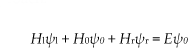
where ψ1,ψ0 and ψr are the wavefunctions of three consecutive unit cells, matrix H1(Hr) denotes the hopping elements of a unit cell of GNR to the previous cell on the left (right), E is the charge energy, and H0 contains the self-energies and eventually the self-generated/external potential. The above approach makes use of well-defined conditions that ensure numerical consistency: all electronic wavefunctions have to be properly normalized, and the excitation ports, i.e., the metal contacts, are to be properly set as transparent, i.e., perfectly absorbing, ports. The physical observables, i.e., charge density and current-voltage characteristics, are derived by energy integrals over the occupied electronic states.
Although some works use density functional theory (DFT) to construct relevant input Hamiltonians, as for instance with four-terminal junctions [9,10], this is not capable of simulating very large devices. However, they become important for small graphene devices, where edge effects are not negligible.
The nonlinear response of graphene Y-junctions arises from the dependence of the conductivity on the Fermi level, which, in turn, depends on the applied voltage [11]. In this perspective, the predicted non-linear response may occur also in devices larger than their ballistic size. This has been shown experimentally [12]. However, the junction nonlinearity may feature specific signatures of the scattering at the junction discontinuity and of transport ballisticity, in contrast to what happens in diffusive or classical devices. In order to visually show the origin of a non-zero voltage in the central branch, with push-pull voltage configuration of the other two branches, let us consider Figure 1. The voltage V2 of branch 2 is actually set to zero; in fact, having a current flowing with V2=0, i.e., metal contact at 0 V, is the same as having V2≠0 with zero current, i.e., open or non-contacted branch. In the figure, I12 is the current from contact 1 to contact 2 and I23 is the current from contact 2 to contact 3. The net current I2 at contact 2 is simply found by I2 = I23-I12.

a) Band structure of the Y-junction; b)
With opposite voltages applied at pot 1 and 3, the current I12 is not, in general, perfectly balanced by current I23, and this leads to a non-zero current at port 2. The reason is explained in the following. Although the potential path of charges coming from port 1 and going to port 2 is similar to the potential path of charges going from port 2 to port 3, the overall potential distributions that they respectively see are actually different, due to the presence of the coupled third branch: for instance, with reference to Figure 1, the path from port 1 to port 2 borders with a low-potential third branch (3), whereas charges from 2 to 3 are confined within a high-potential first branch (1).
The potential in the junction region has been considered in a simplified fashion, i.e., considering it as constant over each of the three branches, but with different values equal to the respective applied voltage. This assumption does not substantially affect the concepts reported in this work.
In some of the cases considered here, we are faced with a second important reason for the imbalance between I12 and I23: the assumption of a central branch wider than the other two branches, as seen in the figure above. This yields different densities of electronic states, directly affecting the current delivered in the three branches. The situation is depicted in Figure 2, where the darker yellow, in the central branch, means a higher density of states; the orange arrow, representing the current I12, originates from a channel with low density of states and points to a branch with higher density, whereas the opposite happens for the green arrow, representing the current I23.
A third effect contributes to complicating the picture: branches 1 and 2 are eventually different from each other, or not symmetrically placed with respect to the central one. Again, this asymmetry may emphasize the nonlinear behaviour by increasing the discrepancy between I12 and I23. In this work, the asymmetry comes from the shape of the unit cell of the GNR branches (see Figure 1(b)), but, in general, other differences may exist: geometry, size, chirality, Fermi energy, metal contact, or doping level. Here, a GNR Fermi level of 0.4 eV in all the GNR branches is assumed.
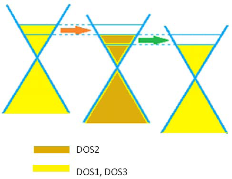
Band structure of the Y-junction: the darker yellow, in the central branch, means a higher density of states associated to a wider branch (DOS2>DOS1=DOS3)
It is observed whether the above three effects cooperate constructively or not; they depend on several parameters, namely the scattering properties among the different branches, and their semiconducting or semimetallic nature. As a matter of fact, simulations suggest that, at the nanoscale, the output of the system, i.e., the voltage at the second branch, is hardly predictable unless a very precise control of the chirality, relative position, and size of the three branches is made experimentally possible.
A general expression for the current flowing from port i to port j of the Y-junction is derived from the Landauer formulation:

where e is the (negative) unit charge, h is the Plank constant, i and j indicate port number, t is the charge transmission coefficient, f is the Fermi function at each port, the integers p and q span the mode channels of port i and port j, respectively.
3. Numerical results
All the following calculations are performed by the scattering matrix approach, as described above.
In Figure 3(a), we report the transmittivity between port 2 and ports 1, 2 and 3, including the contributions of all their electronic channels:

a) Charge transmittivity T2j from port 2 to port j=1,2,3 with respect to the energy; b) sum of the transmittivities of (a)

where the Fermi probability is included in the coefficients.
For completeness, the sum of reflection (T22) and transmittivities from port 2 (T21 and T23) is reported in Figure 3(b), in order to assess the numerical consistence of the calculation: at any energy, the above sum must return an integer number, equal to the number of the (propagating) electronic channels of port 2, for the considered energy (energies are referred to the Dirac point of port 2).
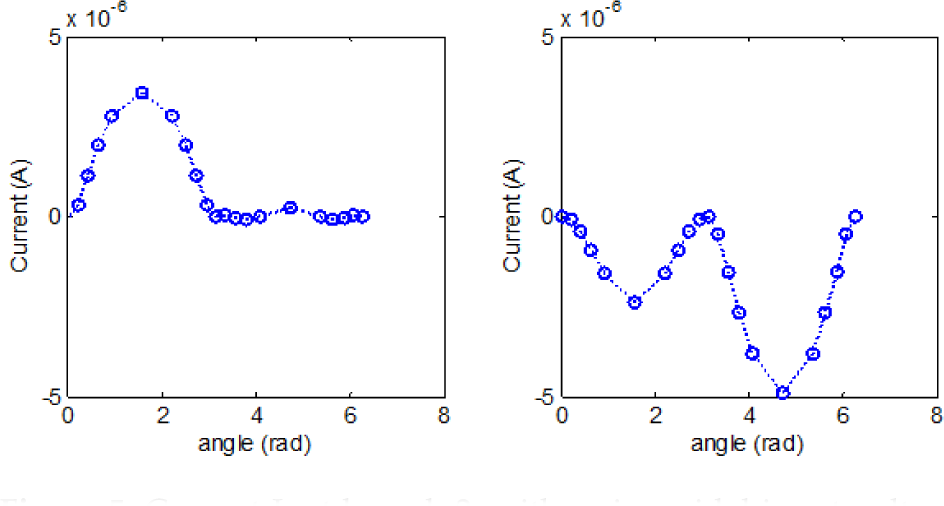
Figure 4 shows the output current I2 at port 2, when a sinusoidal input-voltage is applied between ports 1 and 3, with 0.4 V from peak to peak, i.e., V1-V3=0.2sin(angle), where angle is the phase in radiants.

Current I2 delivered at contact 2, with a sinusoidal input voltage across the ports 1 and 3; left plot:
The output current is not linearly proportional to the input voltage, but looks more similar to the absolute value of the input (with negative sign), and contains a DC component. This suggests the application of the Y-junction as logic port and RF detector [13].
Figure 5 reports the output current I2 as a function of the sinusoidal input voltage V1-V3 as above. The form of the output strongly depends on the scattering properties of the junction, defined, in the central plot, by
Current I2 at branch 2, with a sinusoidal input voltage across ports 1 and 3; left plot:
In the examples of Figure 6, we set

Current I2 at branch 2, with a sinusoidal input voltage across ports 1 and 3; left plot:
As can be seen from the figures above, the output current I2 features high variability, and strongly depends on the scattering properties of the junction, which depends, in turn, on the parameters
4. Conclusions
In this contribution, we report the nonlinear effects of three-terminal graphene ballistic junctions. The ballistic calculation, fully developed by a scattering matrix approach, shows that, at the nanoscale, the behaviour of the junction is strongly affected by even small differences in the junction shape. A self-consistent calculation that accounts for the potential self-generated by the charge scattered through the channel, including bound states of charge, is the subject of a forthcoming paper.
Footnotes
5. Acknowledgements
This work has been supported by the European Project, “Carbon Based Smart Systems for Wireless Applications”, (NANO-RF, n. 318352).