
Abstract
In this paper, the analysis of charge injection from metal to a contacted graphene nanoribbon (GNR) is developed by means of a scattering matrix approach. The charge transport, described by the Schrödinger equation in the 2D domain of the GNRs, is solved, together with the 3D Poisson equation for the potential distribution. Varying the work function of the metal contacted to the GNR, alters the so-called “metal doping”, i.e., the amount of charge in the GNR. As easily expected, this in turn affects the I-V characteristic of a GNR channel across two electrodes. Interesting effects appear as the contribution of GNR sub-band is considered and included in the self-consistent calculation.
1. Introduction
The planar carbon nanostructures, such as graphene nanoribbon (GNR), are fated to become an important alternative to the established silicon devices, as they hold promise for extremely low noise and high speed electronics [1–35]. The limitations of Moore's law in term of physics, but also in terms of manufacturability, flexibility and multi-functionality, have motivated research and development to implement new technologies and new wireless architectures. In this context, the properties of graphene, coupled with CMOS compatibility, offer promise for a new generation of smart miniaturized wireless systems. The electromagnetic response of graphene and graphene nanoribbons under plane wave excitation can be represented by a macroscopic complex conductivity. A spatially non-dispersive model, expressed by an integral in
In general, all the integral expressions mentioned above follow from the knowledge of the graphene dispersion curves and, when non-ballistic behaviour is to be accounted for, of the charge lifetime.
One of the most challenging and not completely understood problems that limits the production and reproducibility of nanodevices arises due to the difficulty of engineering the contact resistance between metal and one- or two-dimensional nanostructures. At the contact, band alignment arises from a self-consistent charge diffusion between metal and nanostructure, and vice versa: equilibrium is reached when the electric potential due to the charge redistribution compensates for the initial difference of Fermi energy at the two sides of the contact. Fermi level alignment, band bending and the Schottky barrier are all consequences of this redistribution of charges, and are relatively easily obtained by standard numerical routines. In such an analysis, the main input parameters are the work functions of the joint materials.
Although the above mechanisms are relatively clear, in nanocontacts involving carbon structures some difficulties arise from the need to account for a multitude of different effects that contribute to the contact characteristics [21–24]: the overall geometry, the operation temperature, the material work functions, the external voltages, the low dimensionality, the lattice orientation, the scattering due to defects/impurities or to other effects such as phonon-coupling and charge interaction. Furthermore, the fabrication process is a key feature as it decides the quality of the nanostructure and of the metal morphology responsible for good charge-coupling. On the experimental side we observe in the literature that very different values of nanocontact resistance can be found even for similar devices.
In the case of GNR lying over a conducting substrate, we address the issue that with just one atomic layer - or a few layers if double or three layer graphene is considered - a continuum of energy states around the Fermi level of the substrate is induced in the GNR by the exponential tails of the substrate wavefunctions. Thus, the GNR Fermi level only aligns to the conductor Fermi level, moving up or down depending on its initial position, and this results in a sort of n- or p-type doping for the GNR [21–23]. Hence, the potential distribution has to be computed accounting for proper boundary conditions at the electrodes, determined by work functions and applied voltages.
Within this relatively simple model, the metal contact produces an n/p-type doping on contacted graphene: the smaller the metal work function, the larger the electron density on the contacted graphene. The electron density in turn affects directly the current-voltage characteristic by means of an increased change injection that means a better ohmic contact. This gives rise to a so-called “induced uniform metal doping”. For instance, nanocontacts of n or p type are simply obtained by using respectively low or high work function metals.
Recently, we have introduced full-wave techniques both in the frequency (energy)-domain [25–32] and the time-domain [33–40] for the investigation of new devices based on carbon materials, e.g., multiwall (MW) CNT, graphene and graphene nanoribbon (GNR). The quantum transport is described by the Schrödinger equation, or its Dirac-like counterpart, for small energies. The electromagnetic field provides source terms for the quantum transport equations that in turn provide charges and currents for the electromagnetic field.
2. Device under test and modelling
In the present work, we use the frequency (energy)-domain method reported in [25–32]. We assume that the e.m. wavelength is small as compared to the charge spatial variation, and that the frequency of the e.m. field is very small as compared to the time dynamic, i.e., the energy of the travelling particles. This kind of analysis can be applied in order to explore the basic working principles of graphene in its use as an interconnect and as a channel for FET. For instance, a lumped circuit model with parasitic capacitances, including the quantum capacitance of the graphene channel, can be easily derived from the simulation results. This leads to a rough estimation of the gain and the unit-gain frequency. In practice, the non-ballistic effects reduce the conductance of the interconnect and the unit-gain frequency of the transistor.
The main result of the present work resides in that it shows, by means of some new examples, the effectiveness of the scattering matrix approach for the solution of relatively large graphene systems involving thousands of carbon atoms and consequent multichannel transport.
In fact, differently from simulations performed at the atomic scale, where it is very difficult to deal with large carbon devices, we consider structures made of many thousands of carbon atoms. Other common approaches that, similarly to ours, avoid ab initio calculation, like Non Equilibrium Green's Function (NEGF), could be successfully applied. The NEGF [24] describes the carrier interaction through a spatial charge density that locally perturbs the graphene neutrality. The scattering matrix approach is equivalent to the NEGF, but, in our opinion, it better highlights the physical behaviour of the system, because: i) it makes use of electronic modes that are easily normalized with respect to the physical current, ii) it considers the physical ports of graphene circuits by the same standard as the virtual ports, i.e., all the accessible electronic wavefunctions, iii) it treats all the ports as adapted ones, i.e., transparent or perfect absorbing, iv) it allows an easy check of the lossless and reciprocity constrains involved in charge transport through the scattering matrix properties, v) it allows the use of concepts well-known in the microwave and RF community, such as cascade of transmission lines, transformers, lumped circuit elements, etc., all useful in order to model long graphene structures eventually containing defect, bending, discontinuities and electrostatic perturbations.
An important parameter for the operation of an FET is given by the gate differential capacitance: this parameter directly affects the frequency characteristics of the transistor as the unit gain frequency. The derivative, with respect to the gate bias of the charge density in the channel after self-consistent solution of the transport/electrostatic problem, provides the channel contribution to the gate capacitance. Some simple models, based on the geometric and dielectric characteristics of the gate and the channel, may provide some partial results, by employing a metallic approximation for the channel. However, it is well-known that the electromagnetic screening is much less effective in two dimensions than in three dimensions, and graphene behaves, to some extent, as an ideal two-dimensional electron gas. Hence, a rigorous analysis must include the knowledge of the actual electronic structure of the GNR channel and its change under external voltage. The result is what is usually referred to as quantum capacitance, that is, the change of the channel energy levels and of the corresponding wavefunction distributions due to an external applied voltage.
The Schrödinger equation is formulated in its discrete version [25]:


One of the difficulties of the proposed method resides in that the scattering formulation has to be adapted to a periodic waveguide, where the right basis to be used for describing charge transport is given by the complete set of Floquet, or periodic, modes. Within the latter choice the scattering parameters can be shown to obey, for example, the expected reciprocity and losslessness constraints, respectively
The number of modes at any port depends on the port size, on the Fermi level and on GNR chirality. Regressive modes, either above or below cut-off, are scattered out of the GNR without reflection: this means perfectly transparent ports.
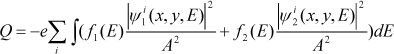
In the case of a two-port GNR, the charge density is obtained by summing the normalized wavefunctions of carriers injected from the two opposite ports:
For a multiport device, all physical quantities are obtained by including the charge contributions from all ports. For instance, the total current flowing through the p-th port includes the contribution of all modes transmitted from port p to all the other ports:

3. Simulation results
According to the model of the metal contact described above, the Fermi level of the GNRs over metal is chosen slightly away from the symmetry point of the GNR dispersion curves, leading to a nonzero charge density. We consider the latter as a free parameter resulting, in practice, from the contact with metals with different work functions.
In the simulations of Fig. 2, the boundary conditions are given by: Vg=0V, V ranges from 0 to 0.4V. Each curve corresponds to a different metal work function, ranging from 4.1eV to 4.35eV. The GNR work function is assumed 4.5eV.

a) GNR-FET; b) definition of mGNR.

a) I-V characteristic for different values of metal work function (W
The iterative Poisson/Schrödinger (PS) scheme requires the 3D potential solution φ, evaluated in the (x,y) plane, to be consistent with the 2D charge density Q, calculated as in (4), that is also a function of x and y. Thus, the target where Si,jpq is the scattering coefficient from mode i to mode j and from port p to port q.
A schematic view of the device under study is shown in Fig. 1a): a semiconducting GNR connects source and drain of an FET-like device. A potential difference of 0.1V is applied between drain and source; the source is assumed at 0V, equipotential with the lateral gate (G). A rectangular waveguide approximation is assumed for the electrodes - see [25] for further detail - and the half space under the GNR is realistically filled by SiO2, whereas air is assumed in the half space above. Figure 1b) shows the armchair GNR considered in this work, with the general definition of a m: in the present case, m=18. solution (Q, φ) has to converge in a two-dimensional domain, point by point. This is a strong requirement and, as a matter of fact, a large number of iterations, i.e., >10, could be needed in order to obtain a stable solution. Moreover, a well-known limit cycle problem may occur when a particular charge density Qn-1 gives rise to a certain potential φ n-1 and, in the next numerical cycle, a different pair Qn and φ n is produced, so that charge and potential simply bounce back and forth from state (n-1) to state (n), never converging. In this case, a different choice of the starting potential should be tried.
In Fig. 3 we report the same curves as Fig. 2, with included information about self-consistency: the self-consistent (dashed) and not self-consistent (dot-dashed) I-V characteristics feature fairly small differences. The potential profile in the GNR, in the non-self-consistent case, is that of the device without GNR.
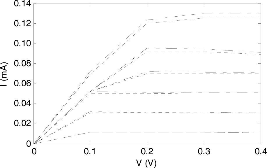
Comparison between self-consistent (dashed) and not self-consistent (dot-dashed) calculation: the difference is quite small.
Figures 2 and 3 above show that the current increases as the metal doping increases, i.e., as the metal work function reduces. There is however an apparently strange behaviour at V=0.1V: in the figure below we mark in red this particular situation where there is no significant sensitivity of the current to the metal work function.
The explanation is quite simple and can be resumed graphically in Fig. 4(b-d), where the arrows point to the higher values of the Fermi level of the contacted graphene, i.e., smaller values of the metal work function.

a) zoom of Fig. 1a at V=0.1V; from b) to d), a decreasing metal work function, i.e., an increasing Fermi level, as indicated by the arrows, is assumed in the calculation.
In the situation of Fig. 4b, marked by a blue circle, an increase of the Fermi level allows more electrons to be injected from the left contact so that the current increases. In the situation c), marked by a red circle, an increase of the Fermi level is ineffective because it allows more electrons to be injected both from the left and right contacts, so that the net current remains unchanged. Actually, the charge density in the channel changes, and, according to self-consistency, also the local potential and the overall I-V characteristic change, but, as already observed in Fig. 3, this effect is not very important. In the situation d), marked by a green circle, again a situation similar to b) is reproduced, but now just involving the second sub-band.
4. Conclusions
In this paper, we consider the debated issue of the metal-to-graphene contact from a numerical point of view. The question of what happens as the metal Fermi level varies is solved numerically, at least for small displacements of the metal work function with respect to the GNR work function. The result is not completely obvious as, in fact, current-voltage characteristics do not simply increase with the above displacement: some more complicated effects are shown to appear as the contribution of GNR sub-bands is included in the calculation. We are currently working on comparing the results from this metal-carbon model with experimental results. Beyond the metal-carbon transition model, we are investigating further features of the presented techniques [25,–40], with regard to using graphene in multifunctional nano- and bio-nano-electronics [41–42]. Among the graphene properties in the THz and optical regime, a very challenging issue to be analysed is the quenching fluorescence of aromatic molecules that seems to be greatly associated with photo-induced carrier transfer [43].