
Abstract
We investigated the effects of dopants on epitaxial growth of Si NWs, with an emphasis on synthesizing vertical epitaxial Si NW arrays on Si (111) substrates. We found that addition of boron with a B:Si feed-in atomic ratio greater than 1:1000 improved the percentage of Si NWs grown along the vertical <111> direction to more than 90%, compared to 38% for i-Si NWs. We also demonstrated a stemmed growth strategy and achieved a 93% percentage of i-Si NW segments along the vertical <111> direction on Si substrates. In summary, our study opens up potential for using chemical synthesized vertical Si NW arrays integrated on Si substrates for large-scale applications.
Keywords
1. Introduction
Silicon nanowires (Si NWs) have been demonstrated to work as building blocks for applications in electronics, optoelectronics, energy conversion, energy storage and sensing [1, 2]. The bottom-up synthesis methods, especially vapour depositions, offer controls at nanoscale in Si NW and nanowire heterostructures, enabling modifications of electronic [3] and/or photonic [4] properties by bandgap engineering. Further integration of nanowires in large-scale applications often requires precise control of the position and orientation of individual nanowires in an array. Vertical Si NW arrays on Si substrates are a desirable configuration as it can be used directly for potential three-dimensional applications, avoiding the time and cost required for post-growth alignment [5, 6]. To this end, epitaxial growth of Si NWs along the vertical <111> direction on Si (111) substrates is of particular interest, as the (111) plane is the lowest energy plane observed for Si, and growth along the <111> direction epitaxially on Si (111) substrates is preferred [7–10], leading to high-yield vertical Si NW arrays.
In order to improve the homoepitaxial Si NW growth along the vertical <111> direction on Si (111) substrates, strategies such as optimization of growth conditions and fabrication of buffer layers to confine the catalyst and the growth have been considered [11–13]. However, specific understanding of effect of dopants on epitaxial growth of doped Si NWs [14], which are essential for operations in electronic applications, is limited. In this work, we investigate the effects of dopants for epitaxial growth of Si NWs on Si (111) substrates, and demonstrate a strategy to improve the vertical growth yield in a Si NW array by exploiting doping effects.
2. Experimental details
Si NWs were synthesized on Si(111) substrates using a chemical vapour deposition. Hydrogen chloride produced by pyrolysis of silicon tetrachloride (SiCl4) has been found to promote the epitaxial growth of Si NWs on Si substrates through reacting with oxide residue [13, 15]; therefore, SiCl4 was used. Au films with 10 nm thickness were deposited on the substrate by an e-beam evaporator after removing the native oxide layer using buffered hydrogen fluoride. After loading the substrate into the quartz tube in the vapour deposition system, we filled up the quartz tube with H2 until the total pressure and the temperature were ramped to the desired 760 Taorr and 850°C, then started growth by flowing a mixture of 45 sccm H2 carrying SiCl4 and 200 sccm H2. SiCl4 flow rate as a function of carrying H2 is given by
Scanning electron microscopy (SEM) images of the grown samples were taken using a field emission SEM (Hitachi S-4800). The top view and tilted view of the samples were utilized to analyse the growth orientation of the nanowires. The angle between the NW axis and the substrate plane in the 90° tilted view and the angle between the symmetrical NW axis in the top view were the key parameters focused on. For instance, on Si (111) substrates, the vertically grown NWs are along the normal direction of the substrate, a <111> direction. Three other <111> directions show an angle of 19.5° to the (111) plane in the side view and 120° between each other in the top view. The <112> and <110> directions show 70° and 55° to the (111) plane.
To reveal the different sections in the stemmed Si NWs, we exploited potassium hydroxide (KOH) etching of synthesized stemmed NWs. Vertically grown stemmed nanowires were first sonicated in isopropanol and dispersed on Si substrates. After removing native oxide on nanowires using buffered hydrogen fluoride solution for 5–10 s, the substrate with nanowires dispersed was immersed in a mixture of KOH (20 wt% in water) and IPA solution with a volume ratio 3:1 at 80°C for 45 s.
3. Results and discussion
Representative as-grown intrinsic silicon nanowires (i-Si NWs) (figure 1(a)–1(c)), and B and P doped Si NWs on Au-coated Si (111) substrates (figure 1(d)–1(f) and figure 1(g)–1(i)) are shown in figure 1. For doped Si NWs, the feed-in atomic ratios of B:Si and P:Si were estimated to be 1:550. We analysed the growth orientations of 174 i-Si NWs in total in the 90°-tilted SEM images, and estimated that the percentage of i-Si NWs grown along the vertical <111> direction was approximately 38%, while 57% of NWs were along the tilted <111> directions. Addition of B2H6 resulted in a substantial increase in the percentage of NWs in the vertical <111> direction, up to 98% of total 118 NWs analysed, as shown in figure 1(d)–1(f). Addition of PH3 seems to randomize the orientation distribution of P-doped Si nanowires, in which 63% of 93 P-doped Si NWs examined were inclined to <112> orientations and 24% were grown along the <110> direction. Note that few P-doped NWs were observed along the <111> directions. The strong dependence of NW growth orientation on the dopant types implies that doping is a key parameter when fabricating arrays of vertically aligned Si NWs on Si (111) substrates. Specifically, the promotion of vertical <111> growth orientation observed from B-doped Si NW growth is remarkable, opening up the potential for the direct assembly of vertical B-doped Si NWs for applications.
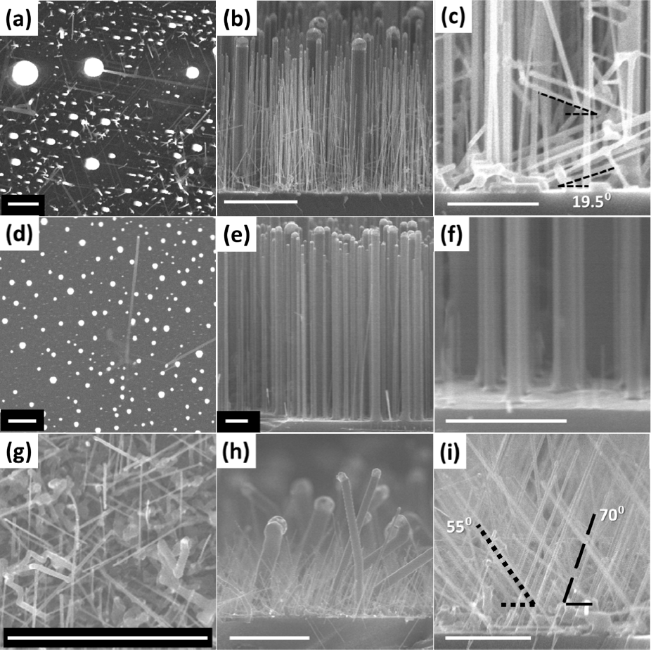
SEM images showing (a, b, c) i-Si NWs, (d, e, f) B-doped Si NWs, and (g, h, i) P-doped Si NWs. (a, d, g) top view; scale bars are 5 μm. (b, e, h) cross-sectional view; scale bars are 5 μm. (c, f, i) magnified cross-sectional view; scale bars are 1 μm. Doped NWs were grown with an atomic B:Si ratio of 1:550 and a P:Si ratio of 1:550, respectively.
To further evaluate the doping effect of B for epitaxial growth, we performed the growth of B-doped NWs when varying the doping concentration. In all trials, the flow rates of H2 carrying SiCl4 were fixed at 45 sccm and the total flow rates of the gas mixture, including H2 processing gas, H2 carrying SiCl

Percentage of vertical Si NWs as a function of B2H6 flow rates. Corresponding B:Si feed-in atomic ratio estimated is also shown.
In order to understand how B2H6 doping contributes to the promotion of vertical wire growth on Si (111) substrates, we first compared the kinetics of i-Si NW and B-doped Si NW growth. The NW growth length as a function of growth time is plotted in Figure 3a for i-Si NWs and B-doped Si NWs with a 1:550 B:Si feed-in atomic ratio. It is notable that growth rates for NWs with different diameters can vary; for instance, a reduced growth rate was observed for smaller-diameter NWs and attributed to the Gibbs-Thomson effect [17]. Therefore we have specifically measured the lengths of NWs with a diameter of approximately 100 nm. Each data point in figure 3 was obtained from 30 vertical NWs. The growth rates of i-Si NWs and B-doped Si NWs were estimated to be 91 nm/s and 106 nm/s, respectively. The faster growth rate observed for B-doped Si NW growth here was consistent with the well-explored phenomenon of dopant-induced growth rate change in thin films [18].
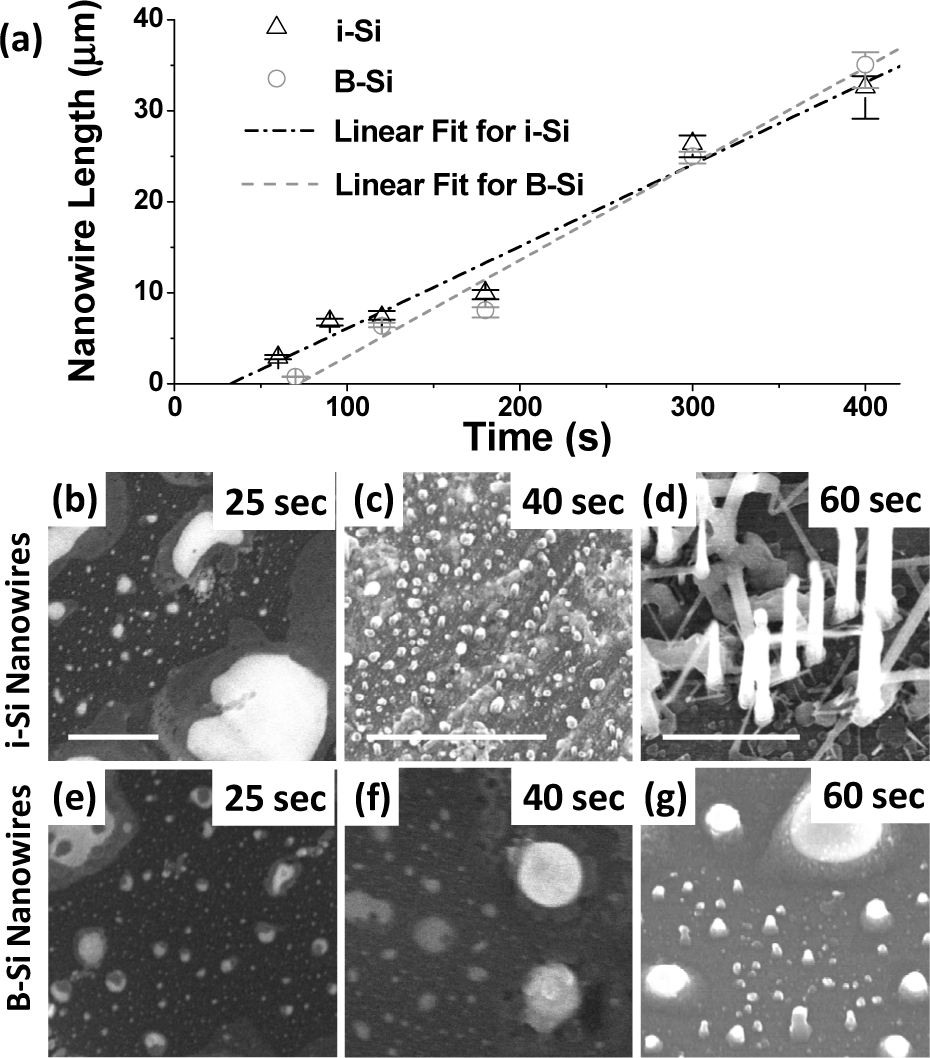
(a) Length of vertical nanowire measured as a function of growth time. (b-g) SEM images of different growth stages for i-Si NWs (b-d) and B-doped Si NWs (e-g). (b-c) SEM observations of different evolution steps of nanowire over reaction time. Growth time is 25 s for (b) and (e), 40 s for (c) and (f) and 60 s for (d) and (g). (a,b) are top view and (c) is 15° tilted view. All scale bars are 1 μm.
The linear extrapolations of the length vs. growth time curves reveal different intersections of the x axis [11], which indicate different nucleation times - the time period required for precipitation of the supersaturated Si from Au/Si liquid alloy [19] - for i-Si NWs and B-doped Si NWs. The nucleation time for B-doped NWs was found to be 71 s, compared to 35 s for i-Si NWs. The presence of highly concentrated B2H6 results in a delay in the nucleation.
To confirm that these differences in nucleation time was not due to fitting of the plot, we captured the SEM snapshots of the samples undergoing different stages in the growth process and terminated by rapid cooling and evacuating the deposition chamber. Si NW growth from Au films is considered to go through three steps: Au film agglomeration, nucleation from the supersaturation of Si in AuSi alloy, and Si NW elongation. As shown in figure 3(b) and figure 3(e), similar morphology changes of Au agglomeration were observed for both i-Si NW and B-doped growth at 25 s after starting of SiCl4. Au films were dewetted and agglomerated, and a broad distribution of the agglomerated Au islands was observed [20]. In the SEM images taken at 40 s into the growth (figure 3(c) and 3(f)), the nucleation of Si was observed for the i-Si NW growth while for the B-doped case the morphology of the Au film remained similar to figure 3(e). At 60 s after the initiation of growth (figure 3(d) and 3(g)), elongation of i-Si NWs with the average NW length measured to be 2.9 μm was clearly observed and B-doped Si NW growth started to show nucleation and initial elongation. Collectively, these snapshots together with the analysis of x-axis intersections highlight that the nucleation in B-doped Si NW occurred after 40 s, a greater delay than in i-Si NWs. We hypothesize that this delayed nucleation facilitates a better interface formation between the epitaxially grown nanowires and the Si substrate, a key factor promoting vertical growth. Phase separation was noticed in some catalyst sites through all stages. We speculate that this was due to the precipitation of dissolved Si from liquid alloy during the cooling step.
A closer inspection by SEM, shown in figure 4, reveals the different shapes of bases for i-Si NWs and B-doped Si NWs. The bases of i-Si NWs observed tend to be more faceted and wider than the body, whereas B-doped Si NWs show a smoother transition at the bases towards vertically grown NW bodies. Such a smooth base morphology is a feature of epitaxial vertical growth. The wider base for i-Si NW can be attributed to the changing contact angle of Au-Si eutectic droplet during growth [20]. The contact angle, for a fixed substrate, depends on the eutectic-air (surface) and eutectic-substrate (interface) surface tensions. For B-doped Si NWs, the eutectic droplet is a ternary mixture of Au-Si-B, which would exhibit surface and interface tensions significantly different from the Au-Si binary mixture. Hence, we expect this to result in a vastly different contact angle, and subsequently give rise to different NW base morphology. For instance, such a change in the surface tension can result in lowered growth rates, as observed in Sb-doped Si NWs [22]. Although the Sb dopant was not introduced during the nucleation stage, this work elucidates the complex phases and substantial surface tension changes in ternary mixtures. Similarly, for P-doped NWs grown under identical conditions, it is reasonable to expect that the change in the contact angle leads to a distinct NW base morphology. Further modelling and studies are required to establish a quantitative understanding of the effect of dopants on surface tension, interface tension and the contacting angle of ternary mixtures, as well as their connection to epitaxial growth orientation.

30° titled SEM images of Si NWs showing the detailed morphology of the bases of nanowire. (a) i-Si NWs and (b) B-doped Si NWs. Growth time for both samples was 3 min. Scale bars are 500 nm.
The doping effect on epitaxial growth of Si NW on Si substrates can be utilized to improve the yield of vertical epitaxial i-Si NWs or lightly B-doped Si NWs in a NW array. To this end, we have developed a stemmed strategy in which i-Si NW segments are grown on B-doped Si stems through axial dopant modulation [23] (figure 5a). A two-step growth process was used: the first step involved growing B-doped Si NW stems (B:Si feed-in atomic ratio = 1:550) for 90 s, and in the second step B2H6 was terminated and main segments of i-Si NW grown for 90 s. SEM imaging and analysis of 80 nanowires produced showed that 93% of stemmed wires were epitaxial and vertical, which is comparable to 98%, the percentage observed for the B-doped Si nanowires (figure 2) and a substantial improvement on 38%, expected from the i-Si NWs (figure 2). To confirm such improvement was due to the stemmed strategy, we performed a selective etching using KOH solution [24]. Figure 5(c) shows representative SEM images of stemmed nanowires after KOH etching, clearly indicating two distinguished segments in each wire: a shorter and thicker segment close to the base corresponding to the B-doped stem, and a longer and thinner one close to the Au tip corresponding to the i-Si segment. The result is consistent with the previously reported etching study showing that the etching slows down drastically or stops for Si with high concentrations of boron (>1019 cm−3) [25]. Further tests also verified that the improved vertical <111> yield of i-Si NW segments was observed as long as the B-doped Si stems were grown for longer than 50 s with a B:Si feed-in atomic ratio of 1:550.
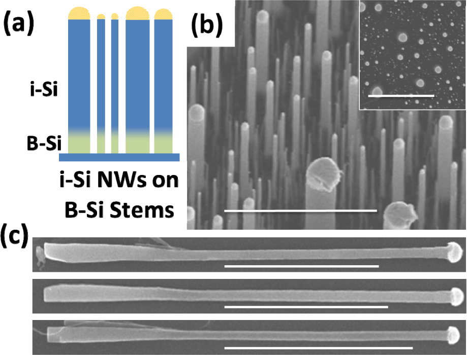
(a) Schematics of i-Si NWs on B-doped Si stems. (b) 15°-tilted SEM images of i-Si NWs on B-doped Si stems; (inset) top view of the sample; scale bars: 5 μm. (c) representative SEM images of selectively etched stemmed nanowires; scale bars are 5 μm.
To promote i-Si NW growth along the vertical <111> orientation, this stemmed strategy was also found to be able to shift the diameter distribution. Figure 6(a) and figure 6(b) demonstrated diameter distributions along the vertical <111>, tilted <111> and other directions for i-Si NWs and B-doped Si NWs. In both cases, broad distributions ranged between approximately 20 nm to exceeding 250 nm. Such broad distributions are expected from Au-film-catalysed Si NWs. Specifically, for i-Si NWs where vertical and tilted <111> are both present, thinner wires prefer the tilted <111> orientations while thicker wires prefer the vertical orientation [11, 15]; consequently, an average 45 nm diameter is obtained for tilted <111> and 103 nm for vertical NWs. Notably, i-Si NWs with diameters less than 50 nm and along vertical <111> orientations, which is a likely desired diameter and the configuration for nanoelectronic applications, only take less than 5%. 12% B-doped Si NWs are thinner than 50 nm and along the vertical direction (figure 6(b)), and are much better represented compared to the i-Si NWs. This result suggests that we can improve the yield of thin and vertical i-Si NWs utilizing the stemmed strategy discussed above. Figure 6(c) confirms that the i-Si NW segments grown using the stemmed strategy show 25% of vertical wires with a diameter below 50 nm.

Diameter distributions of different growth orientations for (a) i-Si NWs, (b) B-doped Si NWs, and (c) stemmed i-Si NWs with B-doped Si bases grown on Si (111) substrates. B:Si was 1:550 in both (b) and (c). Data presented in (a)-(c) were obtained from 123, 135, and 80 nanowires, respectively.
4. Summary
We have investigated the effects of dopants on epitaxial growth of Si NWs, with an emphasis on synthesizing vertical epitaxial Si NW arrays on Si (111) substrates. We found that addition of boron with a B:Si feed-in atomic ratio greater than 1:1000 improved the percentage of Si NWs grown along the vertical <111> direction to more than 90%. Compared to i-Si NWs, a delayed nucleation and a smoother base were observed for B-doped NWs, indicating that kinetics and thermodynamics both contribute to the improved epitaxial growth in the B-doped case. We also demonstrated a stemmed growth strategy, in which i-Si NW segments are grown on B-doped Si stems through axial dopant modulation. Exploiting this stemmed strategy, we have achieved a 93% percentage of i-Si NW segments along the vertical <111> direction on Si substrates, a substantial improvement on the 38% obtained for the i-Si NWs. In conclusion, our study opens up potential for applying chemical synthesized vertical Si NW arrays integrated on Si substrates in large-scale applications.
Footnotes
5. Acknowledgements
The work was supported by the Defense Advanced Research Project Agency (DARPA) award N66001-08-1-2037.