
Abstract
One-dimensional nanostructures of Tin oxide (SnO2) have been synthesized by thermal evaporation method with and with out a catalyst on silicon substrate. The nanostructure growth was carried out by using a mixture of SnO2 and graphite powders at a temperature of 1050°C in nitrogen (N2) ambience. The synthesized SnO2 nanostructures show polycrystalline nature with tetragonal rutile structure. SEM investigation reveals wire-like and rod-shaped nanostructures on silicon substrate, with and without the gold catalyst layer respectively. EDX and TEM observation concludes that the uniform SnO2 nanowires (diameter ∼ 25 nm and length ∼ 50 μm) grow with vapor-liquid-solid (VLS) mechanism whereas, the SnO2 nanorods with varying diameter grow with vapor-solid (VS) mechanism. UV-Vis spectra estimates that the optical band gaps of the SnO2 nanowires and nanorods were 3.92 eV and 3.67 eV respectively. As synthesized single SnO2 nanowire based gas sensor exhibit relatively good performance to ethanol gas. This sensing behaviour offers a suitable application of the SnO2 nanowire sensor for detection of ethanol gas.
1. Introduction
Growth of one-dimensional (1D) nanostructures has attracted increasing attention in recent year due to research and practical applications of these novel structures in next-generation devices and sensors. [1–2]. 1 D nanostructures may be formed in the form of tubes, belts, rods, wires, etc. These structures with high aspect ratio (i.e., size confinement in two coordinates) offer better crystallinity, higher integration density, and lower power consumption. Tin Oxide (SnO2) is an n-type semiconductor with a wide band gap (Eg =3.62 eV, at 300 K) and is well known for its potential applications in gas sensors [3], dye-based solar cells [4], transparent conducting electrodes [5] and optoelectronic devices. The SnO2 nanostructures can be synthesized by laser ablation [6], electro-deposition [7], thermal evaporation [8–9] and rapid oxidation [10]. Among these, thermal evaporation is the most popular method for the growth of nanostructures due to its process simplicity, easy-to-handle equipment, low cost infrastructure and high throughput. In addition, this method can also be used to synthesize several types of nanostructures such as nanowires, nanobelts and nanorods. The morphology and properties of nanostructures is generally determined by the growth parameters such as temperature, carrier-gas flow rate, catalyst layer and type of substrate.
In this paper, we have synthesized SnO2 nanostructures by thermal evaporation method with and without gold thin film on Si substrate. The nanostructures were characterized with different characterization techniques for investigating the effect of the substrates on the structural morphology, crystal structure, composition and optical properties of SnO2 nanostructures. The gas sensing behavior of SnO2 nanostructure is also studied.
2. Experimental Details
(a) Synthesis of SnO2 nanostructures
N-type (100) Si wafer was used as a substrate for the growth of SnO2 nanostructures. First, the Si substrate was atomically cleaned in the following solutions: Isopropyl alcohol (IPA) with ultrasonic vibrations for removing dust and organic substance, a mixture solution of H2SO4 and H2O2 for removing the grease and inorganic impurities, and 10% HF solution for removing the native SiO2. The gold (Au) catalyst thin film (∼ 100 nm) was then deposited on the Si surface in radio-frequency (RF) sputtering chamber at the pressure of 1×10⁻⁶ mbar and 100 watt power. Next, the Tin oxide (SnO2) nanostructures were grown at an elevated temperature by using the thermal evaporation method. The evaporation apparatus used in the present experiment contains a quartz tube mounted inside a horizontal tube furnace. An alumina crucible, filled with analytically pure SnO2 and Graphite (4:1) powder was located at the center of the tube and the Si and Au coated Si (Au/Si) substrates were located at some distance from the source. Then, the carrier gas of nitrogen was introduced into the tube and kept flowing at a rate of 100 sccm and the furnace was heated at 1050°C for 2 hours.
Finally, the substrates were cool down to the room temperature and than unloaded from the furnace. The as-synthesized SnO2 nanostructures were characterized and analyzed by Scanning Electron Microscopy (SEM), X-Ray diffraction microscopy (XRD), Energy Dispersive X-ray Spectroscopy (EDX), Transmission Electron Microscope (TEM) and UV-Vis spectroscopy.
(b) Gas sensor fabrication
The Si substrate was used for sensor fabrication. A silicon oxide (SiO2) layer of about 100nm thickness was thermally grown on Si substrate. Then Au electrodes were deposited on SiO2/Si substrate by using R.F. sputtering process. The Shadow mask was used for electrode formation. The as-grown SnO2 nanowires were scratched, transferred and dispersed in IPA solution by ultrasonication process. These dispersed SnO2 nanowires were transferred on pre-fabricated gold electrodes. This assembly with SnO2 nanowire bridging between sensor electrodes were post annealed in air at 300°C for 1 hour. This fabricated sensor was than used for the study of I-V characteristics and ethanol gas sensing properties of single SnO2 nanowire.
3. Results and Discussion
3.1 Morphology and optical characterizations
Fig. 1 and Fig. 2 shows the typical scanning electron microscopy (SEM) images of the samples annealed at 1050°C for two hours in the N2 ambience. Fig.1 shows that the SnO2 nanowires are homogeneously grown over large area on Au/Si substrates; their lateral dimensions depend on the deposition parameters. The typical length of the SnO2 nanowires is several tens of micrometers whereas, the diameter is in the nanometer range. Fig. 2 shows that the SnO2 nanorods i.e. rod-shaped nanowhiskers are grown on Si substrate. These nanorods grow sparsely on the substrate with several micrometers in length. From this analysis, this can also be observed that the nanowires grow with uniform diameter whereas, the nanorods are having non-uniform diameter. Further insight into the detailed structure of the SnO2 nanostructures is taken by TEM.

SEM images of Tin oxide nanowires grown on Au deposited silicon substrate [Au (100 nm)/Si].

SEM images of Tin oxide nanorods grown on silicon substrate.
The XRD pattern (Fig. 3) reveals the overall crystal structure and phase purity of the SnO2 nanowires and nanorods. All diffraction peaks can be indexed to the tetragonal rutile structure of SnO2 with lattice constants of a=4.740 Å and c=3.190 Å. No characteristic peaks of impurities, such as elemental Sn or other tin oxides, were observed. The strong and sharp reflection peaks suggest that the well-crystallized SnO2 products were successfully obtained through the present synthesis method.

X-Ray patterns of Tin Oxide nanostructures.
Fig. 4 shows EDX spectra of the as-synthesized products on Au/Si and Si substrates annealed at 1050°C for two hours in the N2 ambience. The EDX analysis of SnO2 nanowires on the Au/Si substrate indicates that the synthesized products consist of Au, Sn and O elements and the EDX analysis of SnO2 nanorods on Si substrate indicates the presence of only Sn and O elements, regardless of position in the SnO2 nanostructure. The impurities such as C and Cu in EDX spectra are due to Cu grids and carbon film on Cu grids.

EDX spectra of the SnO2 nanostructures on (a) Au/Si (b) Si substrates.
Fig. 5 shows the TEM analysis of the as-synthesized products on Au/Si and Si substrates annealed at 1050°C for two hours in the N2 ambience. In this analysis, a polygonal shaped particles is found at the tip of the SnO2 nanowires (Inset in Fig. 5 (a)), which demonstrates strong evidence that the growth of SnO2 nanowires is controlled by the vapor-liquid-solid (VLS) mechanism [11] and its diameter was estimated to be 25 nm.

TEM images of single nanostructures of Tin Oxide on (a) Au/Si substrate (b) Si substrate.
The insets TEM image in Fig. 5 (b) shows two nanorods together which represents the non uniform diameter of grown nanorods throughout the Si substrate. Fig. 5 (b) shows the absence of the Au nanoparticle or any other catalyst on the tip of SnO2 nanorods. This supports the fact that the nanorods grow with vapor-solid (VS) mechanism [12] and the diameter of different nanorods was estimated in the range of 80 nm to 350 nm.
The optical bandgap of SnO2 nanowires and nanobelts were investigated using UV-visible absorption spectrometer. Fig. 6 shows UV-Vis spectra of the as-synthesized products on Au/Si and Si substrates annealed at 1050°C for two hours in the N2 ambience. The calculated band gap energy is ∼3.92 eV for nanowires and ∼3.67 eV for nanorods, as shown in the inset of Figure 6. The larger band gap of nanowires than that of nanobelts also agrees well with their lower sizes as observed from TEM analysis.

UV-Vis absorption spectra of the SnO2 nanowires and nanorods. The inset shows the (αhν)2 versus photon energy curve.
3.2 Electrical and gas-sensing properties of single SnO2 nanowire
SEM image of the as-fabricated sensor is shown in Fig. 7 (a) and shows the presence of single SnO2 nanowire between two gold electrodes. Fig. 7 (b) represents current-voltage (I-V) characteristics of the gas sensor in air at different temperatures. The (I-V) curve of as fabricated sensor shows good ohmic behavior. The ohmic behavior is very important to the gas sensing properties, because the sensitivity of the gas sensor is affected by contact resistance. We have measured the I-V characteristics at temperature up to 200°C and found that there is no difference in the I-V curve. The resistance of single SnO2 nanowire was in the range of 50 MΩ.
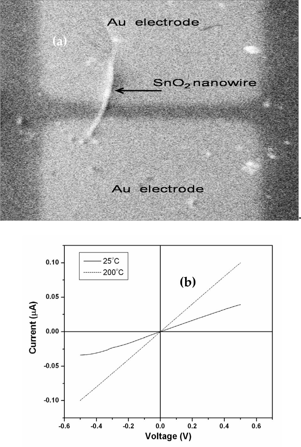
(a) Scanning electron micrograph of as fabricated SnO2 nanowire gas sensor (b) I-V characteristics of the sensor at different temperatures.
The gas-sensor testing was successfully done by using set-up at our laboratory. Fig. 8 shows the schematic diagram of gas sensing measurement setup. During the gas sensing measurement, firstly the sensor assembly is mounted on heater and all connections are made.

Schematic of gas sensing measurement system used in present study.
Then heater is allowed to heat upto 200°C. When heater temperature reaches upto 200°C than we have recorded the response of sensor by using Keithley electrometer and response of sensor is recorded by computer that is connected serially with sensing set up. The response of sensor is recorded in air ambience as well as in the presence of ethanol vapors. 0.5 ml amount of ethanol vaporizes 100 ppm of ethanol vapors in the test chamber of about 5 liter capacities. Fig. 9 (a) shows the responses of SnO2 nanowire sensor under exposure to 100 ppm of ethanol gas at 200°C. This response curve is stable. Ethanol was dropped on the heating element inside test chamber and micropipette was used for this purpose. The ethanol causes a change in the resistance of SnO2 nanowire from 50 MΩ to 20 KΩ, where Resistance in air (Ra) = 50 MΩ and Resistance in ethanol (Rg) = 20 KΩ. The response and recovery time is about 3 seconds and 10 seconds respectively, which is very much less than SnO2 thin films.

(a) Response characteristics of single SnO2 nanowire sensor to ethanol at 200°C. (b) Sensor response as a function of ethanol concentration (c) sensor response for 100 ppm ethanol concentration at different temperatures.
Fig. 9(b) shows the sensor response of SnO2 nanowire gas sensor to various ethanol concentrations at a constant temperature of 200°C.
The different ethanol concentrations of 100 ppm, 200 ppm and 300 ppm are attained by dropping 0.5 ml, 1 ml and 1.5 ml of ethanol in test chamber of 5 liter capacity. The response of sensor is increased linearly with increasing of concentration of ethanol gas with a small fluctuation. This linear dependence offers a suitable application of the SnO2 nanowire sensor for detecting ethanol gas. The linear sensor response (Fig. 9 (c)) is also observed from the response of SnO2 nanowire sensor to 100 ppm of ethanol concentrations at various temperatures.
4. Conclusions
We have demonstrated that the SnO2 nanostructures can be successfully prepared with and without the Au catalyst film on the Si substrate by using the thermal evaporation method. The surface morphology study of the grown nanostructures concludes the growth of the nanowire (uniform diameter ∼25 nm) on the Au coated Si substrate whereas, the growth of the nanorods (varying diameter ∼ 80 nm to 350 nm) on the Si substrate. The synthesized nanostructures show polycrystalline nature with tetragonal rutile structure. The TEM analysis confirms the VLS growth of the nanowires on the Au/Si substrate and VS growth of nanorods on the Si substrate. In addition, the larger band gap of the nanowires than that of the nanorods was also examined by UV-Vis Spectra. The as-synthesized SnO2 nanowires were used to fabricate ethanol gas sensor. As synthesized single SnO2 nanowire based gas sensor exhibit relatively good performance to ethanol gas. This sensing behavior offers a suitable application of the SnO2 nanowire sensor for detecting ethanol gas.