
Abstract
We investigated the morphological and structural change in silicon nanostructures embedded in the silicon oxynitride matrix. The study has been carried out on thin films thermally annealed at high temperature, after deposition at 400°C by Electron Cyclotron Resonance Plasma Enhanced Chemical Vapour Deposition (ECR-PECVD), under different deposition parameters.
Our study evidenced the existence of a well defined threshold for the silicon content in the film (around 47%), to get Si nano-crystallization in the silicon oxynitride matrix. Both Si nano-crystals and Si nano-columns have been observed by TEM analysis in two samples having a similar Si content but deposited under different conditions.
1. Introduction
Nanostructured silicon-based materials have emerged out as a promising system in optoelectronics applications and devices. In particular, silicon oxynitride (SiON) combining various physical properties (such as: optical, mechanical, electrical, etc.) of silicon dioxide (SiO2) and silicon nitride (Si3N4) materials, has attracted considerable attention in optoelectronic industry. This material can be easily deposited at low temperature with the reliable and mature Plasma Enhanced Chemical Vapour Deposition (PECVD) technique.
SiON exhibits low absorbance and adjustable refractive index between 1.46 (SiO2) and 2 (Si3N4) [1] by changing the ratio of precursors gas flow, during deposition. However, these properties can also be suitable for photovoltaic solar cells, especially for the antireflection layer.
In addition, the antireflection layer is not the only possible application of SiON. In fact, due to the increasing price of silicon solar cells, the fabrication technology is oriented to use thinner wafers, thus the quality of the rear passivation surface is becoming increasingly critical for maintaining high efficiency in solar cells [2].
Finally, the search for photo-conducting and luminescent materials compatible with technology processing of silicon-based integrated-circuits is another need for optoelectronic applications, and it has been receiving great attention in recent years [3]. In this respect, silicon rich silicon oxynitride exhibit very interesting features as a luminescent material as well as a dielectric matrix for silicon nanocrystals nucleation [4, 5, 6].
In this work we studied some physical properties of thin films of silicon oxynitride containing silicon nanostructures whose nucleation has been induced by high temperature annealing.
By means of several techniques, we investigated how the deposition process and the thermal annealing affect the final film crystalline structure.
2. Experimental details
The ECR-PECVD, has been used to deposit silicon oxynitride (SiON) films on quartz and silicon substrates. In the deposition chamber, with a background pressure of about 10−7 mbar, the reactive gases have been excited by microwaves at 2.45 GHz. The effect of the rf power addition to the microwave one, during the film deposition, has been also checked.
The SiOxNy films, with different composition, have been deposited by changing the ratio flows, R, of the N2O to SiH4 precursor gases. Two different set of samples have been deposited with two fixed values of the SiH4 flow, 20 sccm (first set) and 40 sccm (second set). R values, ranging from 0.5 to 3, have been obtained by varying the N2O flow.
Both sets have been deposited fixing the Microwave power at 500 Watt, substrate temperature at 400 °C and deposition time at 5 minutes.
All the deposited samples have been thermally annealed at 1100 °C for 1 hour, in an Argon atmosphere, to induce silicon crystallization. A great care has been devoted to control the parameters of the film heating and cooling, during the thermal process.
The relative atomic composition of the layers (Si, N, O, H), before and after thermal treatment, have been obtained from Rutherford Backscattering Spectrometry (RBS) and elastic recoil detection analysis (ERDA).
A Renishaw RAMASCOPE 2000 μ-Raman spectrophotometer, using the 488 nm excitation wavelength of an Ar+ laser has been used for room temperature characterization of annealed films deposited on quartz substrates.
The structural analysis of the annealed films, deposited on silicon substrates, has been performed by using both High Resolution Transmission Electron Microscopy (HRTEM) and Energy Filtered Transmission Electron Microscopy (EFTEM) with a JEOL 2100F microscope operating at 200 kV.
3. Results
3.1 Composition of the SiOxNy films
The atomic percentage of silicon, nitrogen and oxygen, has been investigated by RBS as a function of the gas ratio R, on as-grown and annealed samples belonging to the two sets, both deposited on silicon substrates.
Fig. 1 reproduces the behavior for the set deposited at 20 sccm of SiH4 flow.

Atomic percentage of the main film elements vs R, for as-grown (open symbols) and annealed films (filled symbols) deposited at 20 sccm of SiH4. Broken and continuous lines are only guides to eyes. Squares: Si; circles: O; triangles: N.
Concerning the as-grown samples, the relative Si percentage monotonically decreases from 46% at R = 0.5 up to 28,5% for R = 3, (see the Fig. 1). The R dependence of the nitrogen and oxygen contents show a specular behavior one respect to the other. In detail, the N percentage raises from about 18% at R = 0.5 to about 25% at R = 0.75 and then slowly lowers to 8,6 % for R = 3. On the contrary, oxygen slightly decreases from about 23 % up to 21% in the range 0.5 ≤ R ≤ 0.75, followed by a continuous rise up to about 48% at R = 3.
After the annealing process, the film composition show a behaviour as a function of R and a content value similar to those of the as-grown ones (see the Fig. 1) except for the suddenly reduction of the nitrogen content, for the sample deposited at R = 3, accompanied by a symmetric raise of the oxygen content.
Film composition, experimentally observed, corresponds to that of a silicon rich SiOxNy at low R (R = 0.5), to a quasi-stoichiometric SiO2 at high R (R = 3).
Concerning the set deposited at 40 sccm of the SiH4 flow, film composition shows a behavior, as a function of R, qualitatively similar to the first one, except for a higher Si content 1 and a lower value for the oxygen and nitrogen when compared with those of the first set, at the same R. Together with Si, O and N, all the as-grown SiOxNy films contain also hydrogen. This has been detected by ERDA technique only in the as-deposited samples. In both set of films, the H percentage ranged from about 11% to 17%, with a negligible dependence on the R value. This fact is in agreement with the constancy of the SiH4 flow rate for each group of samples.
Atomic film composition as a function of R, is the result of complex electro-chemical reactions taking place during the plasma deposition, whose detailed description requires the detection and monitoring of all chemical radicals, in the plasma process, such as SiHm, O and N which can react to form energetically favorable bonds, such as the SiHm and Si-O ones [7, 8].
Film composition is directly dependent on the N2O gas flow (and then on R) since the silane flow remains constant for each set. As reported in literature, for high N2O/SiH4 flow ratios (high R values) an excess of O radicals will be present with respect to SiHm ones [7, 8], even if the possible presence of non bonded N atoms in the film matrix has been reported by Alayo et al. [8].
Despite the larger number of N atoms (theoretically double) with respect to O ones, the Si-O bonds will be preferentially formed with respect to Si-N, since the energy of the Si-O bond (799.6 kJ/mol) is higher than that of Si-N one (470 kJ/mol) [9], and it is stable even at high temperature.
This result is in agreement with the behaviour of the O and N content in the film (see the Fig. 1). Decreasing R, the number of SiHm radicals for O ions will increase, causing oxygen deficiency and then the appearance of Si-N and Si-H bonds in the layers. A further decrease of R (R < 0.75) will cause a strong reduction of O and N ions too, making homonuclear SiHm reactions more favorite, leading to the deposition of Si rich SiOxNy:H films [7, 8].
As reported in literature, a lower density of as-deposited silicon oxynitride films with respect to the annealed ones could be due to the partial substitution of Si by H and N, with a possible formation of voids which are occupied by non bonded H and N [8]. H and N desorption, upon the annealing treatment, causes a film densification by a network arrangement which may account for the small difference in the element content at the same R value, before and after annealing [1].
As regard as the film composition after thermal annealing, the behaviour as a function of R remains qualitatively similar to that observed for the as-grown samples, except for the N and O content in the sample deposited at R = 3. The drop of the N content, can be explained with the thermal desorption of not bonded N present in the film matrix and it agrees with the above mentioned mechanism.
In particular, in the as-grown films at R ≥ 2, the available N and O ions increase in the plasma phase, leading to a high number of favored Si-O bonds and an high concentration of non bonded N in the film matrix. During the thermal annealing, film undergoes densification as a consequence of N and H desorption from the matrix. This fact alters the relative content of the film components. Finally, the sizeable increase of the relative O content, in the sample at R = 3, may be the result of a sample oxidation during the annealing since the film structure arrangement and densification makes available more Si dangling bonds to react with the O.
3.2. Raman analysis of SiOxNy films
In order to evidence the presence and features of silicon nanostructures embedded in the silicon oxynitride matrix, Raman analysis has been carried out only on the annealed samples of both sets. Investigation has been accomplished on samples suitably deposited on a quartz substrate and then annealed. The measurement system has been calibrated to the well known peak associated to the mono-crystalline silicon, located at 520.1 cm−1.
The Raman spectra of some films of both sets are reported in Fig. 2.

Raman spectra carried out on annealed samples belonging to the first (SiH4 = 20 sccm) and second (SiH4 = 40 sccm) set.
Crystalline volume fraction (Xc) has been deduced from the following relation [10]:

where Ic and Ia are the integrated Raman scattered intensities of the crystalline and amorphous phase, respectively, and

is the ratio of the Raman diffusion cross-sections for c-Si (Σ c ) to that of a-Si:H (Σ a ) [10]. Since the mean grain size is only few nanometers, we can consider η = 1.0 [11]. Silicon crystalline fraction has been evaluated by using the integrated area calculated by the deconvolution of the Raman spectra. These have been fitted by gaussian and lorentzian peak functions, ascribed to the amorphous and crystalline silicon contribution, respectively [12].
The value of Xc decreases with the raise of R up to R = 1 and then it attains a constant value up to R = 1.5 (see Fig. 3).
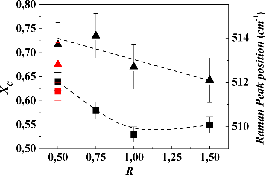
Crystalline fraction (squares) and Si Raman peak position (triangles) as a function of R. Red symbols: samples deposited at 20 sccm of SiH4 flow rate; black symbols: films belonging to the set prepared at 40 sccm of SiH4 flow rate.
Concerning the Raman spectra of the set deposited at 20 sccm of SiH4, an asymmetric peak, located at 512.8 cm−1, is observed only at R = 0.5 and assigned to a Si crystalline phase. At higher R values a broad band appeared, located around 400 cm1, ascribed to the amorphous silicon phase.
Spectra analysis, carried out on the set prepared at 40 sccm of SiH4 flow rate, revealed a linear shift of the Raman peak position, from about 514 cm−1 to 512 cm−1, passing from R = 0.5 to R = 1.5 (see the Fig. 3).
Moreover, for films with R ≤ 1, a broad band located around 480 – 490 cm1 has been also detected and ascribed to the amorphous phase.
The intensity of the Raman peak increases as the R value decreases (see the Fig. 2), due to the increase of the Si content in the film, in agreement with the results of the RBS analysis.
Several groups have observed a shift of the position of the Raman peak associated to the silicon, with respect to the crystalline value located at 520.1 cm−1, in several silicon based materials. This shift has been attributed to the presence of silicon nanostructures and its value has been considered proportional to the mean size of the nanostructure [12, 13].
In our case, based on the electron microscopy observations (see the following section) we have attributed the Raman peak to the presence of Si nanocrystals embedded in the SiON matrix. From the value of the peak shift with respect to the Si bulk crystalline value (520.1 cm−1) we have calculated the average size of the Si nanocrystals by using the following relation [12, 14]:
where Δω(D) is the Raman shift for a nanocrystal with a diameter D, a is the Si lattice constant parameter (a = 0.543 nm), A = 47.41 cm−1 and γ = 1.44 are fitting parameters, reported by Zi et al [12], that describe the phonon confinement in spheres of diameter D. We got values ranging from about (2.0 ± 0,2) nm to about (2.3 ± 0,25) nm, depending on the R value. Using another model proposed by Viera et al [15, 16] we got higher mean sizes, ranging from (3,5 ± 0,3) nm to (4,0 ± 0,5) nm. Even though, these last values are higher than those obtained by the Zi model, they still continue to be lower than those experimentally measured by TEM (see the next section).
The discrepancy between the theoretical predictions and the experimental values in the nanocrystals size has been reported in the literature and ascribed to effects of strain induced in the nanocrystalline structure and/or to a local heating effect in the nanostructure caused by laser excitation during Raman spectroscopy [17, 18, 19].
Several authors [17, 20, 21] have considered the contribution of strain to the silicon Raman peak shift, induced in the nanostructures. Starting from the difference in the nanostructure dimensions obtained directly by TEM analysis and the corresponding value calculated by the Viera model, we have transformed these size differences in a wavenumber shift, A S , by using the following formula:
where Δωexp is the experimentally measured Si Raman shift with respect to 520.1 cm−1; Δω (DTEM) is the expected Si Raman shift taking into account the Viera model for a nanostructure of size DTEM, as measured by TEM.
The uniaxial strain value has been calculated by using the Wolf model, assuming the same parameter of the bulk Si [17]. The estimated values range from 1200 MPa to 1700 MPa. These values are 4
The other possibility to explain the above mentioned differences in the nanostructure sizes, is to take into account the heating effects induced by laser excitation. In fact, the local heating, due to a higher light absorption by the Si nanostructures, causes a broadening and a downshift of the Raman peak position, proportionally to the increase of the local temperature reached by the nanostructure. This effect can mask the shift due to the phonon confinement and sums it up and, if not taken into account, contributes to underestimate the nanostructure size with the currently available models.
In literature, very small Raman shifts has been observed by a laser radiation powers of few tens of μW. At laser powers of few mW, a large shift and a peak broadening have been reported for Si nanowires (NW). In this last case, a Si NW temperature of about 325 °C
In our case, the size of Si nanocrystals (TEM) is slightly larger than the values obtained by the theoretical model of Viera et al. i.e. the Si Raman peak downshift is higher than expected. This fact can be explained by a local heating of Si nanocrystals with respect to the surrounding matrix.
Following the same procedure described above, for the estimation of the strain induced in the nanostructure, we computed the contribution to the Si Raman peak downshift due to the local temperature heating.
As reported by Wolf [17], for every degree of temperature increase, a shift of the Si Raman peak of about −0.025 cm-1 will result. For our samples, the local temperature has been estimated to be 130 °C - 160 °C. These values are lower than those reported in the literature for Si NWs [18, 19] and could be explained with a higher dissipation of the thermal energy for the Si nanocrystals with respect to the Si NWs. In fact, our Si nanostructures are embedded and packed in a SiON network, which allows for a faster dissipation of the thermal energy built up by the Si nanostructures upon laser irradiation, resulting in a lower temperature of the nanostructure.
Finally, based on results obtained by two single effects above mentioned, we can conclude that it's reasonable to assume that both can act simultaneously even if we cannot estimate their relative weight.
3.3. TEM analysis of SiOxNy films
TEM observation, carried out on annealed films deposited on silicon substrates, reveals the presence of silicon nanostructures embedded in the SiON matrix, whose features depend on the deposition parameters. HREM and EFTEM allowed to get additional and complementary features from the investigated films.
In detail, for a sample of the first group (sample A: R = 0.5, SiH4 = 20 sccm) the film exhibits a columnar structure made of crystalline silicon, with a mean diameter of 5÷6 nm, extending from the substrate to the film surface as evidenced in the EFTEM micrography (see Fig. 4).
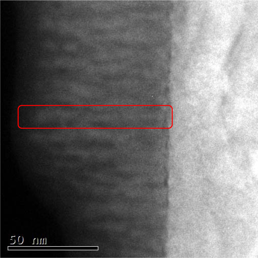
EFTEM micrograph of the annealed sample A (R = 0.5, SiH4 = 20 sccm). Si columns (evidenced by red rectangle) and the SiON matrix appear white graded and dark grey graded, respectively.
This observation agrees with the results of the Raman analysis about the presence of a Si crystalline phase, even though the mean size (diameter) of the Si crystallites is higher than that obtained by the shift of the Si Raman peak.
The crystalline structure of a film of the second set evidences different features. In fact, the electron microscopy observation of a film belonging to the second set (sample B: R = 1.5, SiH4 = 40 sccm) with a Si content similar to that of the sample A, revealed the presence of Si nanocrystals homogeneously distributed in an amorphous SiON matrix (see Fig. 5). The nanocrystals have a mean size of about 5÷6 nm.

EFTEM micrograph of the annealed sample B (R = 1.5, SiH4 = 20 sccm). Si nanocrystals appear white graded while, the SiON matrix, dark grey graded.
The structural differences in the two analyzed samples can be related to the different Si crystalline fraction, higher in the case of the sample A with respect to the sample B, (see the Fig. 3). The higher value of Xc, in the sample A, may result in a coalescence of the Si nano structures to form continuous nano-columns. This fact seems to be supported by the value of the column diameter, showing a mean size comparable to the mean size of nanocrystals observed in other samples.
4. Discussion
The compositional and structural analysis carried out for the two sets of samples suggests the existence of a well defined range for the silicon content in the film to get silicon nano crystallization upon thermal annealing.
In fact, considering the set at 20 sccm, we observed nanocrystals only in the sample with R = 0.5 corresponding to a Si content of about 50%. However, increasing the R value, silicon decreases to about 43% for R = 1, and the lacking of the characteristic Si Raman peak indicates the absence of Si nanocrystals.
For annealed films of the set deposited at 40 sccm, the Si content is always higher than about 47% and in all the samples we found the Si crystalline phase related to the excess of silicon.
Taking into account these results, we can deduce that to induce silicon nano-crystallization, the Si content in the SiOxNy films must be higher than 47%.
However, the silicon content is not the unique parameter responsible of the final structures exhibited by the annealed SiOxNy films. In fact, the TEM micrographies of the two samples A and B, having a similar composition 2 , evidence a different Si crystalline structure: columnar for the sample A and nano-dots for the sample B. This structural difference, related to dissimilar values both of the SiH4 flow rate and R, is related to different reactions of the dissociated precursor gases in the plasma phase with the film surface, occurring during the deposition process.
A comprehension of the reactions involved during the film deposition, requires the monitoring of all the radicals present in the plasma phase.
5. Conclusion
In this work, we have studied the process of Si nano-crystallization in SiOxNy thin films undergone to high temperature annealing. The film composition has been changed by varying the N2O/SiH4 gas flow ratio (R), during the deposition. Two sets of samples have been prepared as a function of R, at 20 sccm and 40 sccm of the SiH4 flow.
We found that the composition of SiOxNy layers can be varied gradually from silicon rich silicon oxynitride to a quasi stoichiometric silicon dioxide, by changing the R value.
Our investigation evidenced the existence of a narrow threshold of values for the silicon content, from about 47% to about 50%, in order to induce nucleation of crystalline silicon nanostructures upon thermal annealing. TEM analysis evidenced the homogeneous nucleation of Si crystalline nanostructures embedded in the SiOxNy host matrix. However, the nano-crystallization can take different routes depending on the other deposition parameters. In particular, crystalline Si columns set in at a SiH4 flow rate as low as 20 sccm, and for a Si content in the film around 47%.
On the contrary, Si nano-dots have been detected at a SiH4 flow rate of 40 sccm, at a Si content of about 50% practically equal to the value of the first set, within the experimental errors. These different structures can be accounted for considering a different reaction of the precursor gases in the plasma phase with the film surface, during the film deposition.
Our study suggests that the absolute value of the SiH4 flow may play a relevant role to determine the final form of the silicon nanocrystalline structures embedded in the SiOxNy matrix.
Footnotes
1
At R = 0.5, Si content attains a value of 59% and 66.7% in as-grown and annealed films, respectively.
2
The composition of the two samples after the thermal annealing can be considered nominally identical within the experimental errors of the RBS analysis.