
Abstract
The metal molybdenum (Mo) thin films deposited on flexible substrates can act as the contact electrode of flexible Cu(In, Ga)Se2 or Cu2ZnSn(S,Se)4 solar cells. In this work, in order to enhance the structural and electrical characteristics of flexible Mo thin films, a negative substrate bias was applied during the direct current sputtering of Mo thin films. The flexible substrates used for growing the Mo films were stainless steel foils and polyimides. The characteristics of Mo thin films were studied by x-ray diffraction and sheet resistance measurements. The measured results reveal that an optimal value of negative substrate bias can be found for improving the electrical and structural characteristics of Mo thin films on flexible substrates. The minimum sheet resistances of Mo thin films are 2.50 Ω/sq and 2.73 Ω/sq for the stainless steel foil and polyimide substrates, respectively.
Introduction
The compound thin films, such as MoS2, LaB6, ZnO, and GaN, have attracted great interests for many years because they have potential applications in optoelectronic device, sensor, Lithium-ion battery, and thermoelectric device, etc. (1-2-3-4-5-6-7-8-9-10). In addition to the compound thin films, the element thin films have also attracted attention. For example, the metal molybdenum (Mo) thin film has been widely utilized as the back contact for Cu(In, Ga)Se2, Cu2ZnSn(S,Se)4, or other sulfides thin film solar cells (11-12-13-14-15). The Cu2ZnSn(S,Se)4 and Cu(In, Ga)Se2 solar cells on flexible metal foil or polymer substrates are new topics in recent years (16-17-18). These flexible thin film solar cells show advantages of softness, high value of power to mass ratio, and reduced thickness, etc. It can extend the application fields of solar cells and contribute to the development of photovoltaic technologies. However, the conversion efficiencies of Cu2ZnSn(S,Se)4 and Cu(In, Ga)Se2 solar cells on flexible substrates are still lower than those of solar cells using typical soda-lime glass substrate (19, 20).
For the flexible Cu2ZnSn(S,Se)4 and Cu(In, Ga)Se2 thin film solar cells, before the preparations of absorbers, the Mo electrodes were first deposited on the surface of metal foil or polymer substrates. The electrical and structural characteristics of Mo electrodes affect the optoelectronic performances of flexible thin film solar cells. Therefore, studying the fabrications and properties of Mo thin films on flexible substrates is helpful. However, up to now, there are only few reports about the Mo thin films on flexible metal foil or polymer substrates (21-22-23).
In previous works, the Mo thin films were sputtered on the surface of different flexible materials (23). By the characterizations of the prepared thin films, we found that the stainless steel foil and polyimide are the most suitable metal foil and polymer substrates, respectively (23). However, the performances of the fabricated Mo electrodes still need to be further enhanced for thin film solar cell application. In present work, we tried to apply substrate bias during the sputtering process to improve the electrical and structural characteristics of Mo thin films on flexible stainless steel foil and polyimide substrates.
Experimental procedure
The stainless steel foils (SUS430) and polyimides (Upilex-50S) with a thickness of 50 μm were selected as flexible substrates. First, all the flexible substrates were successively cleaned in acetone, absolute ethyl alcohol, and deionized water by ultrasonic method. After drying, the substrates were transferred to the magnetron sputtering system. The sputtering source material was a Mo target. The purity, diameter, and thickness of the Mo target were 99.95%, 6 cm, and 3 mm, respectively. The base pressure of the chamber before sputtering was evacuated to be less than 4 × 10⁻⁴ Pa. During the deposition process, the working gas was pure argon (flow: 20 mL/min) and the pressure of the chamber was kept at 5 × 10⁻¹ Pa. The substrate heating was not performed. The negative bias ranging from 0 to 200 V was applied to the substrates. The Mo thin films were simultaneously deposited on the surfaces of stainless steel foil and polyimide substrates by direct current sputtering. The power and deposited time of sputtering were 51 W and 38 min, respectively. As measured by the surface profilometer, the thicknesses of all the prepared thin films were about 1 μm.
The structural characteristics of the prepared thin films were measured by x-ray diffraction (XRD). The x-ray diffractometer was Rigaku D/MAX-Ultima IV using Cu-Kα radiation with a wavelength of 0.154 nm. The voltage and current in the XRD measurement were 40 kV and 40 mA, respectively. The electrical properties of the prepared thin films were measured by four-probe meter (Four Probes Tech, RST-8) at room temperature. The probes were put in direct contact with the surfaces of the thin films.
Results and discussion
The measured XRD patterns of the flexible thin films without substrate bias and with different negative substrate biases are given in Figure 1. In Figure 1A, for the thin films on stainless steel foil substrates, the diffraction peaks of iron(Fe) come from the substrates. Since the XRD peaks of Fe and Mo do not overlap, the appearance of Fe peaks does not influence the characterization of deposited thin films. Matching with the standard diffraction data of Mo (PDF#65-7442), the peaks located at 2θ = 40.5°, 73.6°, and 87.6° are indexed to the (110), (211), and (220) planes of Mo structure, respectively. Except the Mo thin films with a substrate bias of 100 V, the preferred orientation of all other thin films is the (110) plane, which agrees with our previous work and other reports (21-22-23-24-25). When the substrate bias is 100 V, the Mo thin film shows a larger intensity of (211) peak than that of the (110) peak. The measured results of XRD suggest that Mo thin films can be successfully deposited on stainless steel foil substrates with different substrate biases.
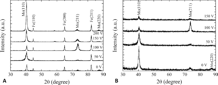
The XRD patterns of Mo thin films with different substrate biases on (
For the polyimide substrates, the thin film with an applied substrate bias of 200 V curls severely and the reason is still unclear right now. It is hard to perform XRD measurement for this thin film. In Figure 1B, the Mo peaks can be also detected in all the XRD patterns. After applying the substrate bias, the (110) peaks in the XRD patterns become weaker than the thin film without substrate bias. When the substrate bias is 100 V, the (211) peak is stronger than the (110) peak, revealing the transformation of the preferred orientation of thin film.
The impact of substrate bias on the structural properties of the prepared Mo thin films is further studied. Figure 2 shows the intensity of the preferred peak and the grain size as function of the substrate bias. Using the full width at half maximum and position of the preferred peak, the grain sizes of thin films are calculated by Debye-Scherrer equation. In Figure 2A, the Mo thin films on stainless steel foil substrates show enhanced peak intensity when a substrate bias is applied. The peak intensity of thin film with a substrate bias of 200 V is about 4 times that of the thin film without substrate bias. However, the grain size of thin films reduces slightly after the application of substrate bias.
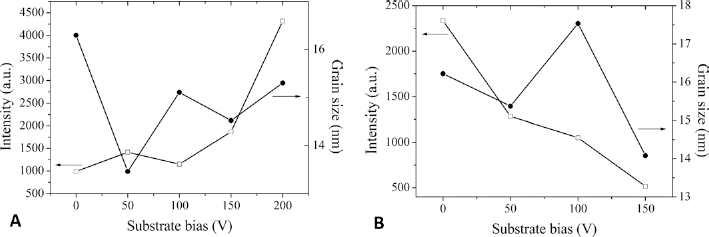
The intensity of preferred peak and the calculated grain size with the substrate bias on (
For the thin films on polyimide substrates, the peak intensity reduces obviously with increasing substrate bias. In addition, the substrate bias has no distinct positive effect on the grain size of thin films. In contrast to the thin films on stainless steel foil substrates, the Mo thin films deposited on polyimide substrates show degraded crystalline structure after applying the substrate bias.
Figure 3 shows the average sheet resistances of the deposited thin films on both substrates against the substrate bias. As mentioned by Xu (23), the stainless steel foils contribute to the measured results of electrical properties. However, both the Mo thin film and stainless steel foil play roles of back electrode for solar cell. The measured sheet resistance can be used for the characterization of electrical properties of Mo electrodes. As seen in Figure 3, for the stainless steel foil substrates, only a substrate bias of 50 V causes a reduced sheet resistance of 2.50 Ω/sq, but the standard deviation is large. Compared with the thin film without substrate bias, the reduction of average sheet resistance caused by the substrate bias is only 5.3%. The Mo thin films with substrate bias of 100, 150, and 200 V have larger sheet resistance than the thin film without substrate bias. On the other hand, the substrate bias is an important factor for the reduction of resistances of thin films on polyimide substrate. All the Mo thin films with substrate bias on polyimide substrate show lower average sheet resistances. Besides, the standard deviations of sheet resistance are lower than that of the thin films deposited on stainless steel foil substrates, indicating the uniformity of thin films on polyimide substrates. When the applied negative substrate bias is 100 V, the average sheet resistance of thin film reduces to 2.73 Ω/sq, which is only 57% to that of the thin film without substrate bias.
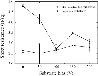
The average sheet resistances of molybdenum (Mo) thin films with different substrate biases on stainless steel foil and polyimide substrates.
As we know, when a negative bias is applied on the substrates, the positive ion Ar+ will bombard the surface of the deposited sample. It can clean the thin film surface, leading to the increasing compactness of the deposited thin films. Besides, it can remove the sputtered atoms with lower energy, which is beneficial to the properties of thin films. However, a much more intense bombardment can damage the surface of thin film, resulting in the increasing surface roughness. Therefore, there exists an optimal substrate bias for the sputtering of a thin film. In this study, the two opposite roles of substrate bias result in the complexity of the changes in crystalline structure and sheet resistance of thin films with the negative voltage of substrate bias. By adjusting the negative voltage of substrate bias, the characteristics of flexible Mo thin films can be improved. The electrical properties are more importance for the Mo thin films because they act as the contact electrode of thin film solar cells. Hence, in present work, the optimal substrate biases are 50 V and 100 V for the stainless steel foil substrate and polyimide substrate, respectively.
Conclusions
The metal molybdenum thin films were sputtered on stainless steel foil and polyimide substrates. During sputtering, a negative substrate bias was applied. The impacts of negative substrate bias on the characteristics of Mo thin films on flexible substrates were studied by the measurements of structural and electrical properties of thin films. The XRD results show the formation of Mo structure on both substrates. The intensity of XRD peak and grain size of thin films can be enhanced by applying a suitable substrate bias during the sputtering process. By adjusting the substrate bias, the minimum sheet resistances of flexible Mo thin films are 2.50 Ω/sq and 2.73 Ω/sq for the stainless steel foil and polyimide substrates, respectively. The improved characteristics of Mo thin films are ascribed to the increasing atom energy and compactness in the thin film surface. The application of substrate bias during sputtering is a useful way to further enhance the structural and electrical characteristics of flexible Mo thin films.
Footnotes
Financial support: This work was supported by National Natural Science Foundation of China (No. 61504029) and Doctoral Starting up Foundation of Guangdong University of Technology (No. 15ZK0011).
Conflict of interest: The author has no financial interest related to this study to disclose.