
Abstract
Pure and 6% alkali-doped NiO thin films (alkali A = Li, Na, K) were prepared by a sol-gel spin coating method and deposited on glass substrates. XRD analysis showed that the prepared films belonged to a cubic structure with (111) plane as preferential growth orientation for undoped and K-doped samples and (200) for Li and Na doping. An optical study based on (UV-Visible) showed that the band gap tends to decrease with alkali doping and achieves a minimal value with Na doping. The Urbach energy increases systematically with the decrease of the optical band gap. The resistivity measurements showed that alkali doping led to a significant decrease in the resistivity value. The lowest value was achieved for the 6% Na-doped sample. Structural, optical and elastic properties of pure and 6% A-doped NiO were performed using the first principal method based on density functional theory. The optimization of the geometry of the studied samples revealed that the lattice parameters changed after doping. The band structure and density of states calculations showed that undoped and alkali doped samples exhibited an indirect band gap and the doped samples had comparatively narrower band gaps. The elastic constants Cij, Bulk modulus B, Shear modulus G, Young modulus, and Poison ratio of doped and alkali-doped NiO were further investigated.
Introduction
Recently, an increasing interest has been devoted to nickel oxide thin films owing to their high chemical stability, non-toxicity [1] its magnetic, electrical, and optical properties [2] as well as, for their potential applications like, solar cells [3], electrochemical capacitors [4, 5], gas sensors [6], fuel cells and electronic devices [7]. Nickel Oxide thin films can be prepared using a variety of processes such as RF sputtering [8], spray pyrolysis [9] pulsed laser deposition [10], and the sol gel spin coating method which is one of the widely used technics, it is distinguished by a number of distinctive features including: low coast, environment friendly and ease of adjusting. [11]. Despite its experimental ease of preparation, nickel oxide constitutes a real challenge for theoretical study because of the strong interatomic correlation created by its incomplete d shell which poses a difficulty to DFT theory that is based on simplifying many body problems into non-interacting one particle problem by assuming the delocalization of the valence electrons, neglecting the interatomic correlation caused by the ionic core,thus the DFT theory predicts metallic characteristics for NiO [12].
To defeat this deficiency many theories such as GW approximation [12, 13], hybrid density functional like B3LYP [16], Hartee Fock (HF) [14], selfinteraction corrections (SIC) [15] and DFT+U [17], have been developed. by introducing the on-site Coulomb repulsion and the exchange interactions between the 3d electrons to the DFT Hamiltonian [18]. Nickel oxide is one of the few p-type oxides with a band gap of 3.6 to 4 eV [19]. Its stoichiometric form exhibits an insulating character with a resistivity of 1013 ohm.cm [20] and its p-type conductivity that appears in the non-stochiometric form comes from Ni2 + vacancies and Oxygen interstitial [21]. Doping with alkaline atoms (Li, Na, K) is an appropriate approach to reduce NiO resistivity by introducing more charge carriers (holes).
In the last few years, doping NiO with alkaline atoms (Li [22, 40]), (Na [23]), (K [24, 25] was extensively studied, however, all of these studies focused on the dopant concentration effect.
To our knowledge, the effect of dopant type on the physical properties of nickel oxide has not been studied before.In order to enrich this field of research, we performed a comparative study of the structural, optical and electrical properties of 6% Li, Na and K doped NiO thin films prepared by sol gel spin coating method.
Our findings were supported by a theoretical investigation of the structural, electronic and elastic constants performed by the density functional theory (DFT) method. For band structure and density of states calculations the Hubbard U correction was introduced.
Experimental and theoretical methods
Experimental procedures
Pure and 6% A-doped NiO thin films (A = Li, Na, K) were prepared by the sol gel spin coating method. To prepare the precursor solution, 0.2 M of Nickel nitrate hexa-hydrate (Ni(NO3)2.6H2O) was dissolved in a mixture of 80% ethanol and 20% of distilled water. The solution was stirred for two hours at ambient temperature. During stirring (Mono Ethanolamine) MEA was added to the mixture as a stabilizer in a molar ratio of 1 : 1 to nickel nitrate amount. The acquired solution was kept for ageing for one day at room temperature. Doping solutions were made by adding Lithium nitrate, potassium nitrate and sodium nitrate to the above mixture to prepare Li-NiO, K-NiO and Na-NiO samples. Our thin films were grown on glass substrates which were cleaned with acetone, ethanol and finely with distilled water to ensure it is free from any grasses or contaminations. The prepared solution was dropped on the substrate and spun at 2500 rpm for 30 seconds.
Then the film was heated at 220°C for 10 min to evaporate the solvents. The above procedure was repeated eight times. Finally, the prepared films were annealed at 500°C for 2 h to enhance their physical properties. The same procedure was followed to prepare all the samples. The structural studies were based on XRD characterization using CuKα (λ= 1.5418 Å) radiation with 2θ values of varying from 20° to 90°, with the steps of 0.02°. The Optical properties such as transmittance and band gap were obtained by using a UV-Visible spectrophotometer in the range of 300 to 1100 nm wave length. Finally, the measured resistivity values were carried out by using four-point method, using “Jandel RM 3000” apparatus at room temperature.
Calculation methods
The quantum mechanics program Cambridge Serial Total Energy Package (Castep) [26] was used to investigate the structural, electrical and optical properties of Ni0.9375Q0.0625O (Q = Li, Na, K). Kohn-Sham formation based on the density functional theory (DFT) was used to perform the calculations [27]. Generalized gradient approximation (GGA) in the Perdew Burk-Eruzerhof scheme was used to treat the exchange and correlation potential [28]. Pseudo atomic calculations was applied at Ni 3d8, O 2s2 2p6, Li 1s2, Na 2s2 2p6, K 3s2 3p6. The Ultra-soft pseudo potential approach was taken to model the ion electron interactions [29]. For all compounds, plane wave basis set energy cut-off was taken at 500 eV. The Brillouin zone was sampled by employing the monkhort pack method [30] with a separation of 0.05/A°. Geometry optimization tolerances were set as follows: the difference of the total energy is within 5×10⁻⁶eV/atom. The maximum force is 0.01 eV/A°. The maximum stress is 0.02 GPa and the maximum displacement was 5×10⁻⁴ A°. Furthermore, more k-points are required to precisely explore electrical and optical properties, and denser k-points are formed. In addition, the number of conduction bands is a significant element in the computation, as it determines the energy range covered and the number of conduction bands. The precision of the Kramers-Kronig transform is determined. There are 15 vacant bands in the current work. To more precisely define the electronic structure, the DFT+U approach was adopted by employing the Hubbard U correction which treats more accurately the strong correlation between the Ni 3d electrons. Hubbard U values were chosen to be 14.0 eV for Ni 3d, 0.0 eV for Ni 2p, and 6.0 eV for O 2p. For the dopant atoms (Li, Na and K), Hubbard U was set by the default values.
Results and discussion
Experimental results
XRD analysis
Figure 1 shows the x-ray diffraction patterns of pure and 6% A-doped NiO (A = Li, Na, K) thin films which were prepared under the same experimental conditions via the sol gel spin coating method. These patterns show diffraction peaks at 2θ= (37.4, 43.4, 63.0, 79.6) which corresponds to (111) (200) (220) and (222) crystal plans respectively. The indexed peaks are fully corresponding with NiO cubic phase (JCPDS-00-047-1049). For pure and K-doped NiO it is noticed that the (111) crystal plane has the highest intensity representing the preferential growth orientation of the crystal, while it is not the case for other dopants patterns (Li and Na) in which the (200) crystal plane had the highest intensity. In addition, we do not notice the presence of any peaks of impurities, which confirms the purity of the prepared samples.
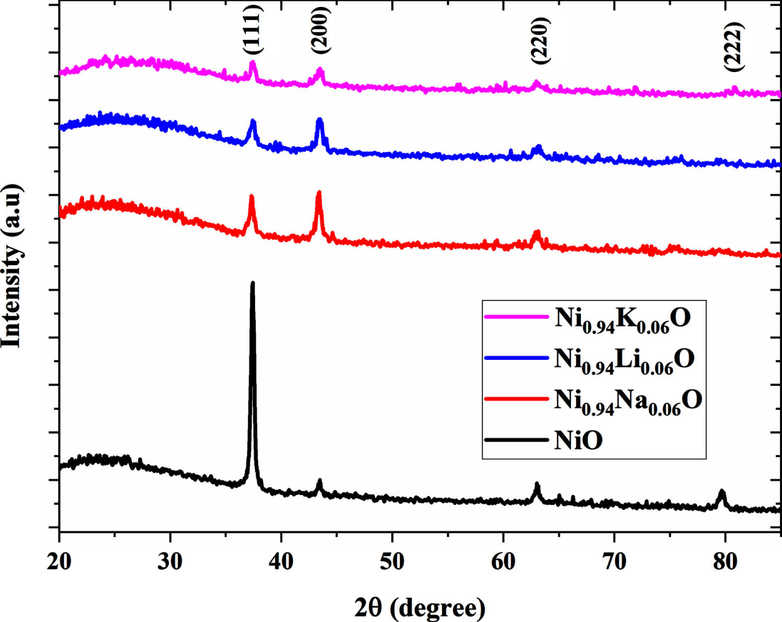
XRD patterns of undoped and 6% A (A = Li, Na, K) doped NiO thin films.
The inter planar spacing dhkl and lattice parameter ‘a’ have calculated using the following relationship [31, 32]:
(hkl): are Miller indices of the crystal planes.
The doped samples have a higher lattice constant value than the pure ones. This is because the ionic radius of the doping atoms (Li+ 0.076 nm, Na+ 0.102 nm, K+ 0.138 nm) differs from the ionicradius of the nickel atom (0.069 nm). This can be attributed also to the external strains resulting from the external defects and vacancies created by dopants incorporation [33].
When compared to the pure sample, the intensity of the peaks of doped samples decreases while increasing in width which could be considered a sign of deterioration of crystal quality [34]. Many crystal parameters, including grain size G, dislocation density, and micro strain, can be derived from XRD data, using the following relationships respectively [31, 66]:
Were k is the shape factor constant (0.9), θ hkl is Bragg angle, and β hkl is the peak broadening.
Calculated crystallite size, strain and dislocation densities are listed in Table 1. Doped NiO samples have a smaller average crystallite size than pure NiO ones. C. Suryanarayana et al. have reported that the growth of grain size is inhibited because the dopant elements accumulate at the grain boundaries during the nucleation [35]. This could be explaining by the large difference in ionic radii between the dopants and Ni2 + . Also the high amount of defects and vacancies created by dopants and which is defined as the length of the dislocation line per unit [36]; contribute to reduction of the grain size values of the doped samples, thus the increase of strain and dislocation density. The K- doped NiO sample has the largest dislocation density and strain values. According to Jansons et al. [37], grain size variations caused by doping are attributable to the thermodynamic barrier to development and this is because the surface dopants influence crystal surface energy. It was found that the incorporation of dopants affects the lattice parameter and leads to limit the growth of nano-particles and increases lattice distortion by introducing more defects such dislocations. The DRX analysis revealed that the 6% Na-doped NiO sample shows the lowest lattice distortion and defects density values.
Structural and electrical parameters of undoped and 6% A doped NiO (A = Li, Na, K)
The measured resistivity values of undoped and 6% A doped NiO (A = Li, Na, K) are listed in Table 1. It is found that 6% alkali-doping NiO has led to a lowering in the resistivity values significantly. It is well known that undoped NiO exhibit a p-type conductivity, which originates from nickel vacancies and oxygen atoms that occupy interstitial sites. This leads to the formation of Ni3 + ions [22, 44]. Doping nickel oxide with Alkali atoms, results in forming more Ni3 + ions, as illustrated in the equation below [22, 45]:
Doping nickel oxide with alkali atoms creates more Ni3 + ions and therefore, the resistivity of the material would be decreased. It should be noted that microstructural defects such as dislocation and grain boundaries affect the mobility of the carriers; in another way they affect the resistivity of the sample since the resistivity is proportional to the reciprocal of the carrier mobility. However, increased dislocation and grain boundaries in the lattice leads to a decrease in the mobility and subsequently to an increase in the resistivity of the thin film [24]. That could be the reason behind the reduced resistivity value of the Na-doped NiO sample (0.38×10⁴ ohm.cm) compared to Li-doped NiO (1.812×10⁴ ohm.cm) and k-doped NiO sample (1.875×10⁴ ohm.cm). The obtained resistivity data match very well with the XRD data. The resistivity values of our samples are lower than those obtained by I.Sta et al. [22] which are prepared by the sol gel spin coating method. This decrease in electrical resistivity is essential for solar cell applications, in which reducing cell series resistance is required. Besides; many applications require Transparent conducting films where the transmittance should be as high as possible in the visible region to enhance the photo-generated current [41].
Optical transmittance of pure and 6% A-doped NiO (A = li, k, Na) in the range of wavelength between 300 and 1100 nm are shown in Fig. 2. Over the visible range, the pure NiO film has a comparatively high transmittance of 85% –95%. The obtained average transmittance of undoped NiO (85% –95%); matches very well with the average transmittance of undopedNiO prepared by sol gel spin coating obtained by Lou et al. [46] and higher than those prepared by spray pyrolysis technique obtained by [41]. The transparency of the doped samples is lower than that of the undoped ones, however the average transmittance of the K-doped NiO sample was found to be about (50%) and about (45%) for the Li-doped NiO sample. The Na-doped NiO sample exhibits the lowest transparency (38%) in the visible region. This decrease in transmittance is attributed to the increase of defects, micro strain, and impurities levels in NiO host lattice after doping [24], also, this decrease could be due to the surface Plasmon excitation and the roughness caused by the growth of grain size [47]. Also, photon absorption by free carriers may contribute to the decrease in optical transmittance [41]. The electrical study revealed that the Na-doped NiO sample exhibits the lowest resistivity and thereby the highest free carriers’ concentration, which could explain the extreme decrease in Na-doped NiO sample transparency. Li and K doped NiO samples have a high degree of transparency with an enhanced electrical conductivity, making them ideal for optical window applications [38]. We notice a red shift in the absorption edge with doped samples compared to the pure ones.
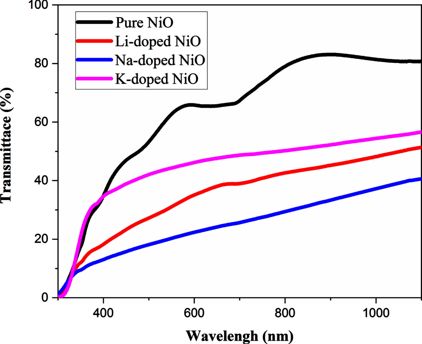
Transmittance spectra of undoped and 6% A-doped NiO thin films (A = Li, Na, K).
The optical band gap (Eg) of the prepared samples was established by the following relationships [32, 39]
Where:
α: the absorption coefficient.
T: Transmittance.
d: film thickness
K: proportionality constant
Figure 3 shows the plots (αhν)2 vs hν. Eg values were calculated by extrapolating the straight-line portion of the plots to the energy axis. Different Eg values are listed in Table 2.
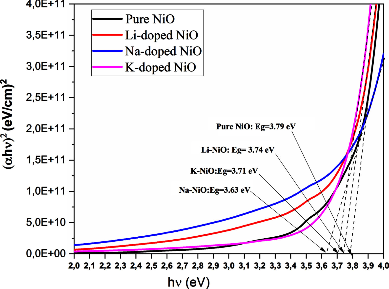
(αhν)2 vs. (hν) of undoped and 6% A-doped NiO thin films (A = Li, Na, K).
Experimental and theoretical band gap + Urbach energy values of undoped and 6% A doped NiO (A = Li, K, Na)
The calculated band gap values of doped samples were found to be lower than those of the undoped NiO samples. The obtained band gap values for undoped NiO are in good agreement with reported data [31, 32]. The Structural study based on DRX analysis revealed that doping NiO with Li, Na or K atoms had led to a decrease in the average crystallite size. It is well known the decrease in crystallite size is usually accompanied by an increase in the amount of the defect. These defects create further energy levels, thus the electronic transition which used to occur from the filled valence band to the empty conduction band; is going to happen from the filled valence band to the defect’s energy levels, creating more band tail states and leading to band gap narrowing [41]. It is found that the band gap of Na-doped NiO (3.63 eV) thin film is narrower when compared to those of K-doped NiO (3.71 eV) and Li-doped NiO (3.74 eV). Y.R. Denny and al [23] has attributed the decrease of the band gap value of Na-doped NiO compared to undoped NiO thin films to the Na 3s states situated over the valence band edge of nickel oxide which results in the lowering of the band gap values of Na-doped NiO sample. As mentioned above, the electrical study revealed that the Na-doped NiO sample exhibits the lowest resistivity and thereby the highest free carriers’ concentration which means that the density of impurity energy levels above the valence band edge would be higher, and consequently the band gap became smaller. The obtained band gap value of the K-doped NiO (3.71 eV) sample is in good agreement with the band gap value of (6%) of K-doped NiO (3.73 eV) prepared via rapid pyrolysis sol gel technic obtained by C.Q. Liu [24]. These results confirm the successful incorporation of dopants in the NiO lattice. The decrease in band gap values of 6% of Na-doped NiO thin films makes them suitable for optoelectronic devices [38].
The same thing as the optical gap, the urbach energy is also related to the disorder in the film network, as it is expressed as follows [42]:
Where α0 is constant and Eu is the urbach energy, it was also determined by the curves of Lnα as a function of photon energy hν is used to deduce the urbach energy
The calculated Urbach values of the doped NiO sample are higher than that of the undoped sample. Lattice distortion and increased microstrain values caused by the incorporation of dopants in the host lattice of nickel oxide may be the main reason behind the increased Urbach energy of doped samples compared to undoped NiO according to XRD analysis. A critical point in the present study is that the Urbach value of the Na-doped NiO sample exhibited the highest Urbach energy values despite having the lowest micro strain and dislocation values. As mentioned above, that could be due to the high carrier concentration value that creates more energy states in the band gap. This leads to more broadening of the Urbach tail, which would result in a decrease in the optical band gap. A quick look at Fig. 4, which displayed Urbach energy and optical band gap values, allows us to note that the increase in Urbach energy matched well with the decrease of the band gap values. In another way we can notice that urbach values and band gap values correlates very well.
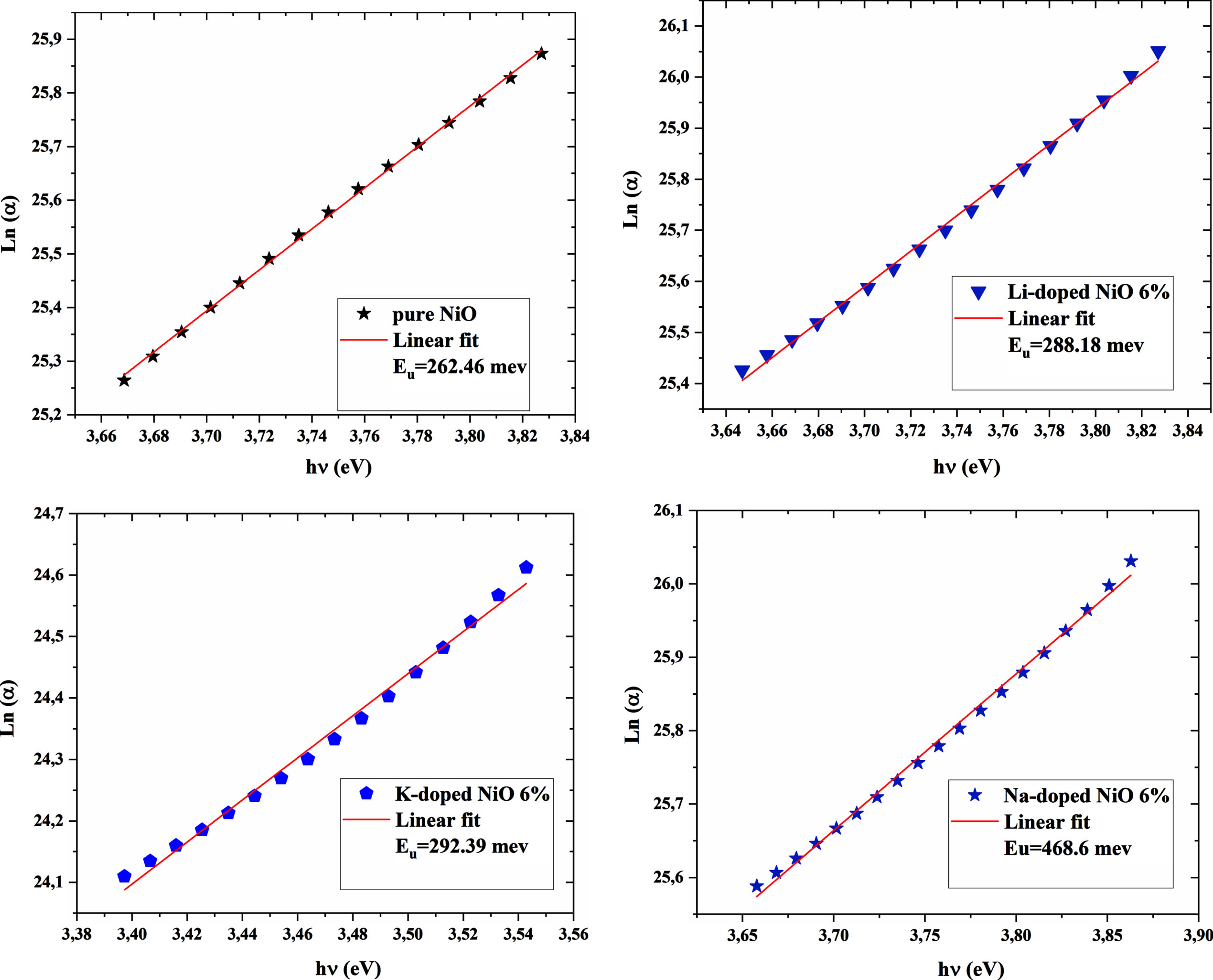
Ln(α) vs. (hν) plots of undoped and 6% A-doped NiO thin films (A = Li, Na, K).
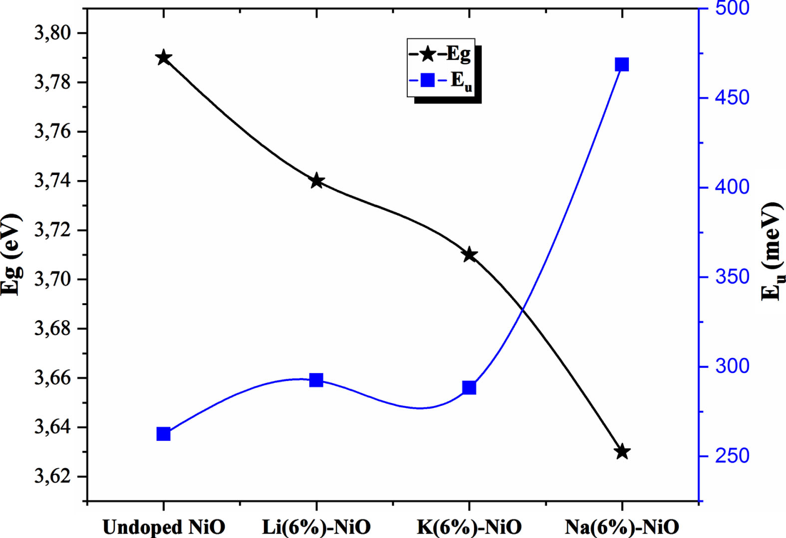
Comparison of band gap and Urbach energy values.
The crystal structure of Ni0.9375A0.0625O (A = Li, Na, K) models were obtained by submitting 6% of A atoms (A = Li, Na, K) for Ni atoms based on NiO crystals. Cubic NiO belongs to the Fm3m space group with a lattice constant of a = b = c = 0.4168 nm and α=β=γ= 90°.
The models of undoped NiO and Ni0.9375A0.0625O (A = Li, Na, K) are shown in Fig. 6a and 6b. Undoped NiO model was calculated in a (111) super cell which contains 4Ni atoms and 4O atoms, whereas the doped NiO super cell is (221) with 1A atom (A = Li, Na, K), 15Ni atoms and 16 O atoms. The Broyden–Fletcher–Goldfarb–Shenno (BFGS) minimization method was used to calculate the structural parameters. The calculated lattice constants after the geometry optimization are reported in Table 3. It can be seen that the theoretical and experimental lattice parameters agree very well. It should be noted that the theoretical lattice constant of undoped NiO obtained in the present work is more accurate than that obtained by J. Xiang [49] and other works [50, 51].
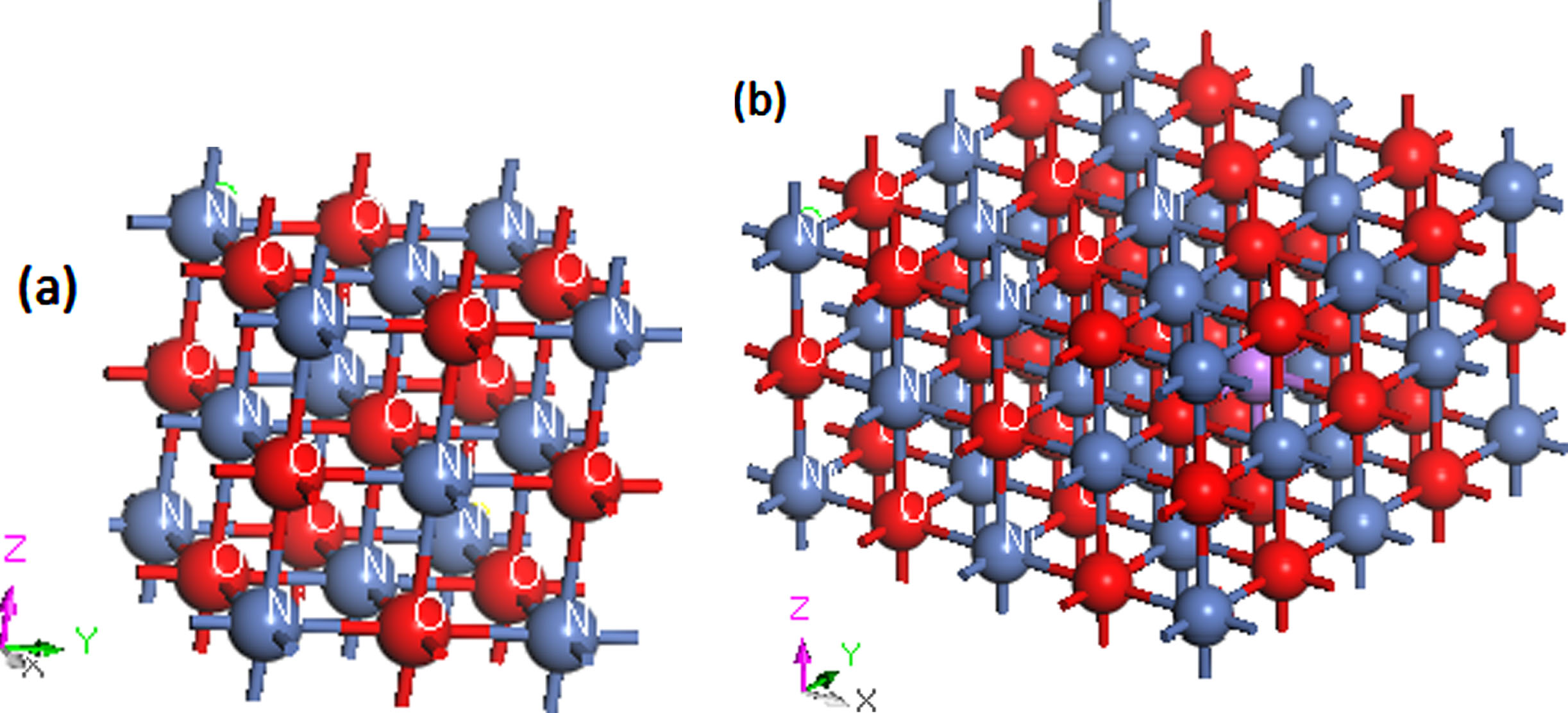
(a) Rock salt structure of undoped NiO. (b) Model of Ni0.9375A0.0625O (2×2×1) (A = Li, Na, K).
Elastic constants of undoped and 6% A doped NiO (A = Li, Na, K)
a[56] d[57] c[52] b[58] e[59] f[60] g[61] h[62] i[63] k[48].
We note that the lattice parameter increases with K and Na doping and decreases with Li doping. This variation is attributed to the dopants radius however K(0.137 nm) and Na (0.102 nm) atoms exhibit an ionic radius higher than that of Ni (0.065 nm), while the ionic radius of Li(0.076 nm) is close to that of Ni (0.065 nm).
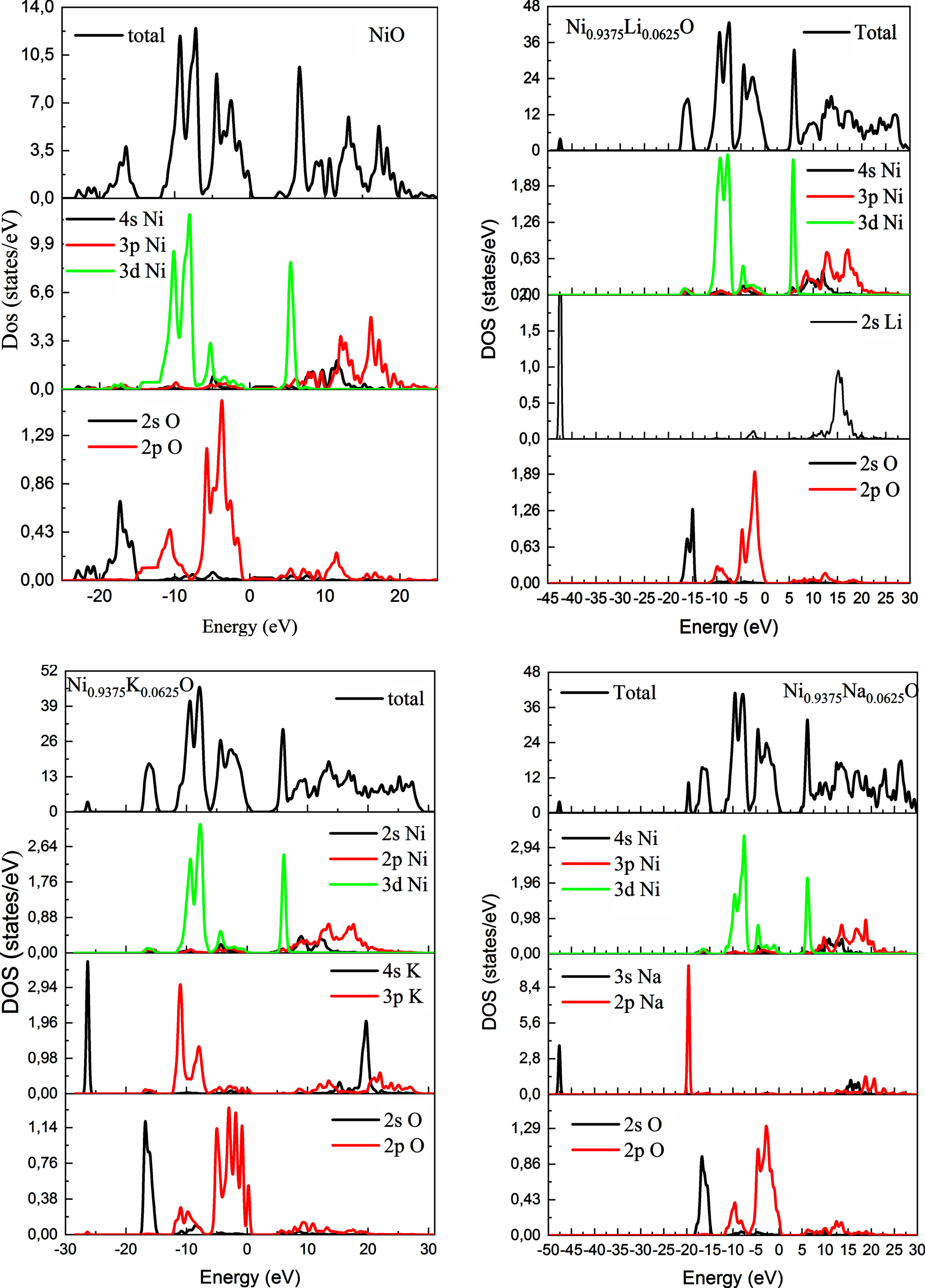
Figure 7 shows that the calculated band structure of pure and doped NiO exhibit an indirect band gaps. The calculated band structure of pure NiO has a band gap of 3.72 eV. The calculated value of pure NiO is very close to the experimental band gap value obtained in this work (3.97 eV), and more accurate than the theoretical data in other DFT calculations [43]. The incorporation of impurities in the NiO host lattice has led to changes in band dispersion near the Fermi level. Where we noted the localization of some bands above the Fermi level, which led to the dispersion of the insulating character nickel oxide band structure. This could be attributed to the DFT efficiency in dealing with the highly correlated systems. In order to manifest the contribution of every atom in the band structuring of each sample, the total and partial density of states of undoped and alkali-doped NiO were plotted in Fig. 8.
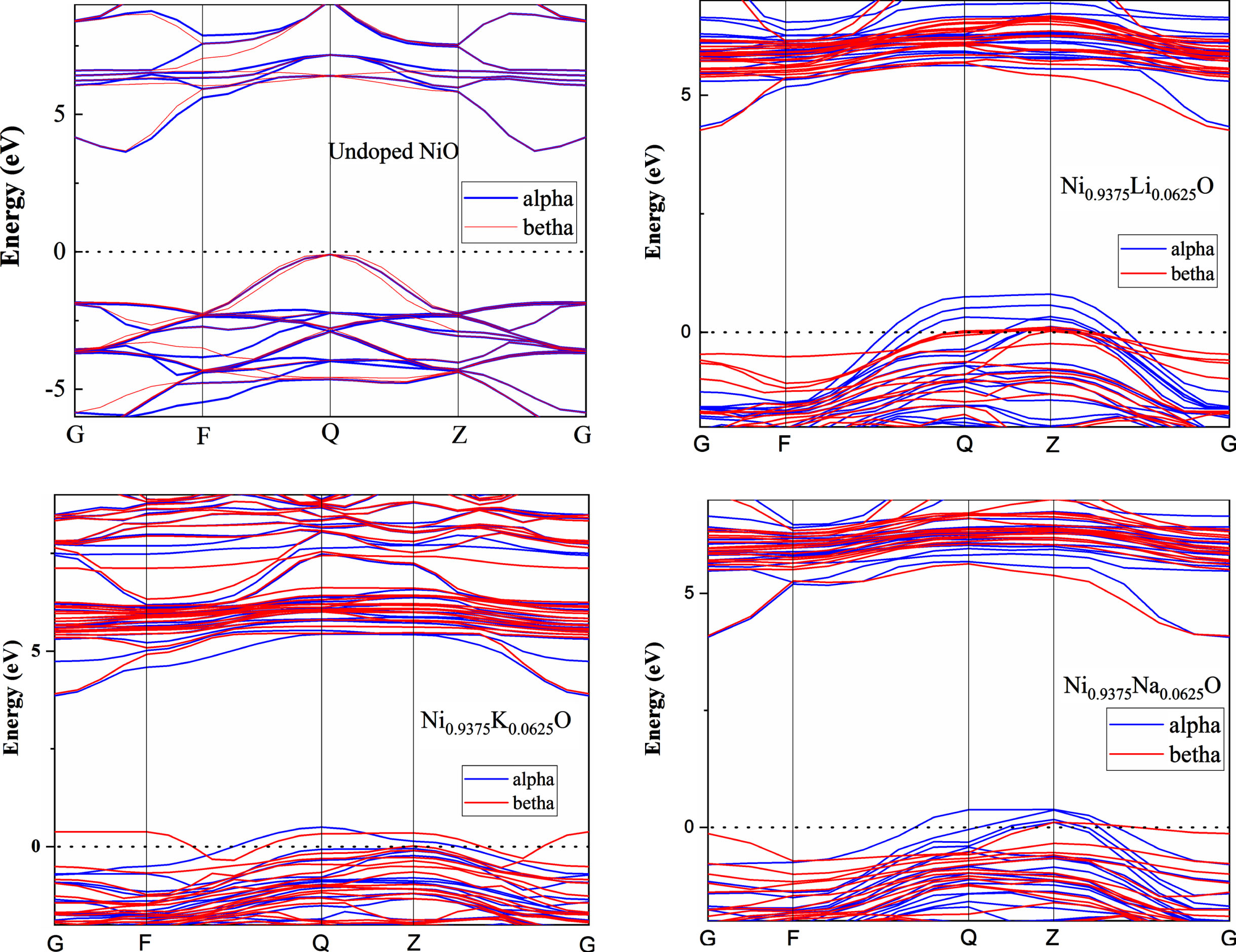
Electronic band structure of undoped and 6% A doped NiO (A = Li, Na, K).
Density of states of undoped and 6% A doped NiO (A = Li, Na, K).
The band structure of both NiO and Ni0.9375Q0.0625O (Q = Li, Na, K) is shown in Fig. 7. The VB maximum (VBM) and the CB minimum (CBM), showing that these materials is an indirect band gap semiconductor. Figure 8 shows the total and partial density of states (DOS) for NiO and Ni0.9375Q0.0625O (Q = Li, Na, K). Accordingly, the band gap (Eg) for pure NiO is about 3.73 eV slightly lower than the experimental value (3.8 –4 eV) [31, 32]. The whole spectrum is mainly dominated by Ni 3d states, except for the interval from –2 eV to EF (0 eV) where the O 2p states are more intense (see Fig. 8). Ni 4s states have a negligible contribution and are not shown. When Li is present, the contribution to the total DOS comes mainly from Ni 3d and O 2p states. The contribution of Li 2s states is negligible. In spite of their low occupation, it is clear that the incorporation of Li in the lattice has a significant impact on the electronic structure.
The top of the valence band is composed mainly of O2p states and that the bottom of the conduction band is dominated by Ni 3d orbitals. It may be expected that Na and K would modify the valence band edge (p-type doping) or introduce impurity states into the band gap because of different p orbitals arising between Na, K and O atoms. For Na doped NiO, we find that the bands originating from Na 2p states locate just above the VBM of NiO while less Na 2p states locate at the CBM simultaneously. On the other hand, the Fermi level EF located above the Na 2p states means that these impurity bands are fully occupied and cannot act as recombination stites. This would serve to reduce the photon transition energy significantly for electron transfer from these states to the CBM. This process induces a narrowing of the band gap, leading to a value of 3.63 eV which is significantly smaller than that of pure NiO (3.73 eV). For K doped NiO (Fig. 8), there are some impurity bands introduced above the VBM while some lie in the band gap; further, some of these locate below the CBM. All of these lead to a significant reduction in the band gap to a value of around 3.33 eV.
It is well known that the semiconductor properties are strongly related to the strain, local and global deformation of the crystalline lattice structure. In which, every deformation leads to a modification of the relative position of atoms which affects the semiconductor properties. Studying the elastic constants of a material allows us to predict how much its structure is stable [44]. Usually, elastic constants are defined employing a Taylor expansion of the total energy E(V, δ) for the system concerning a lattice strain δ of the primitive cell volume V. The energy of a strained system is expressed as follows [45]:
Where E(V0, 0) is the energy of an unstrained system with equilibrium volume V0, τi is an element in the stress tensor, ξi and ξj are factors to take care of the Voigt index. There are three independent elastic constants for cubic (rocksalt structure), i.e., C11, C12, and C44, each of which represents three equal elastic constants (C11 = C22 = C33; C12 = C23 = C31; C44 = C55 = C66).
The requirement of mechanical stability in a cubic structure leads to the following restrictions on the elastic constants [44]:
The computed elastic constants Cij of undoped and alkali-doped NiO are listed in Table 3. As we know, there is no reference in the literature which dealt with these constants. Thus, the results obtained in this paper promise predictor data for future investigations. Obviously, from the calculated Cijvalues above, restrictions are satisfied implying that undoped and A-doped NiO [Ni0.9375A0.0625O (A = Li, Na, K)] are mechanically stable.
The obtained results in this work agree well with the previous theoretical and experimental [56, 63] reports for the undoped NiO with the existence of a little discrepancy between the obtained C11 values and the experimental data. This discrepancy is the result of the complicated description of the correlation between the 3d electrons of the Mott type insulator [52]. Obviously, from calculated Cijvalues above, restrictions are satisfied implying that undoped and A-doped NiO are mechanically stable.
From Table 3, it was found that C11 is higher than C44 for pure and doped NiO, thus we deduce that compression resistance is higher than shear resistance in these materials. C11 measure the a direction resistance to linear compression. As seen in Table 2, C11 of Ni0.9375Li0.0625O is the highest value, while C11 of Ni0.9375K0.0625O and Ni0.9375Na0.0625O are lower than C11 of undoped NiO. So we deduce that doping NiO with Li atoms enhances the compressibility of the a axis unlike doping with 6% Na and 6% K atoms which led to a decrease in the compressibility of the a axis in NiO structure. It was found that the calculated C44 of undoped and 6% alkali doped NiO are relatively low, according to Kube et all, the low value of C44 is belonging to the d-band-filling in transition metal alloys [53].
The Voigt-Reuss-Hill approximation allows calculating the bulk (B) and shearing (G) modulus using the formula below [44]:
However, the bulk modulus B describes fracture resistance, and shear modulus G plastic deformation resistance of the material. The calculated bulk modulus and shear modulus are tabulated in Table 3. From Table 3, the bulk modulus values show that doped NiO compounds are more compressible than undoped NiO. The Na-doped NiO compound is the most compressible. Li-doped NiO and Na-doped NiO compounds have a shear modulus value higher than undoped and K-doped NiO. Stiffness is an important elastic property defined by Young’s modulus as follows E = (9BG)/(G + 3B). As seen in Table 3 Young’s modulus of doping NiO with Na and Li atoms leads to increase Young’s modulus contrary to K doping which led to decrease in the stiffness value. The elastic anisotropy A is a significant on the existence of micro cracks in the solids [54], it is defined by the following relation ship A = 2C44/(C11 –C12). The elastic anisotropy A = 1 means that the crystal is isotropic and anisotropic when A differs from 1. It can be noticed from Table 3 that all the samples show an anisotropic character with A values different from 1. The proportion B/G is related to ductility or brittleness; however the critical value that distinguishes between ductile and brittle is around 1.75 [28.55]. For all the compounds, the value B/G was higher than 1.75, therefore pure and 6% alkali doped NiO are ductile compounds. According to our knowledge, there are no data available in the literature concerning the elastic constants Cij, bulk (B), shear (G), Young’s modulus(E) and B/G of the A-doped NiO[Ni0.9375A0.0625O (A = Li, Na, K)]. Our results are predictions and may serve as a reference for future experimental investigations.
Pure and 6% alkali doped NiO films were prepared by spin coating method. Results showed that pure and 6% K-doped NiO samples are polycrystalline cubic structure with preferential growth orientation (111), and (200) for 6% Li and Na doped NiO. The sample of 6% Na doped NiO showed a better crystallinity compared to 6% Li and K doped NiO films. The optical gaps decrease with alkali doping and it achieved a minimal value with Na doping, while Urbach energy has an opposite variations. The 6% Na doped NiO sample exhibited the lowest value of resistivity.
The first-principles calculation had shown the energy band gap close to energy at the absorption edge. Based on the predicted values of elastic constants, the polycrystalline such as bulk modulus, shear modulus, Youngs modulus, Poison ratio, B/G ratio, and elastic anisotropy were estimated. We showed that the studied compounds are ductile.
All in All, our comparative study revealed that the elastic, electrical, and optical characteristics of the 6% Na-doped NiO thin films are sufficiently equivalent, making it an excellent choice for optoelectronic applications. This work had motivated that the experimental phenomenon could be explain fundamentally via first-principle method.