
Abstract
Tin oxide (SnO2) thin films were deposited on glass substrates using a cost-effective spin coating method. The effect of solution molarity on their microstructural, optical, and electrical properties was investigated. For this purpose, solutions of tin chloride salt were prepared with various molarity in the range of 0.1M to 0.25M. The synthesized films structure and morphology were characterized by different techniques such as X-ray diffraction and scanning electron microscopy. The optical and electrical properties were studied by mean of UV-Vis spectroscopy and four probes conductivity measurement. The X-ray diffraction patterns of all samples revealed well-crystallized and pure SnO2 films with tetragonal rutile structure. The scanning electron microscopy images reveal a smooth and dense film pinholes free. The optical analyses show that the films exhibit an optical transparency that reaches up to 98% in the visible range and that the optical band gap decreases from 3.97 to 3.82 eV when the concentration increases from 0.1M to 0.25M. The films’ electrical conductivity varies in the range from 76 to 100 (Ω cm)–1. The largest figure of merit of 9.8 × 10⁻³ was measured in the films prepared at low solution concentration.

Introduction
Semi-conductor thin films have attracted increasing interest among researchers due to their promising applications in diverse domains principally in electronic semiconductor devices including integrated circuit chips, micro-fabricated mechanisms, micro-electromechanical systems (MEMS), micro-electronic optical systems, as well as light-emitting diodes (LEDs).1,2 Transparent conducting oxides (TCOs) are a class of semi-conductor materials with visible transparency and high electrical conductivity. These properties make TCOs good candidates for opto-electric devices such as electrochromic indium tin oxide (ITO), cadmium oxide (CdO), tin oxide (SnO2), indium oxide (IO), aluminum doped zinc oxide (AZO), undoped zinc oxide (ZO), and fluorine doped tin oxide (FTO). 3 Among these TCOs, tin oxide, SnO2, is one of the most important semi-conductor materials due to its excellent properties (high optical transparency (T ⩾ 85%) and a large electrical conductivity that can be tailored by doping with foreign atoms), non-toxicity, stability in heat treatment.4,5 It is a n-type semiconductor with a large optical gap ranging between 3.91 and 4.03 eV. 6 All these properties make the SnO2 films excellent candidate for various applications including: transparent conducting electrodes, liquid crystal displays, photovoltaic cells, thin-film heaters, and solid-state gas sensors.7,8 However, to obtain oxides thin films with interesting properties, to develop novel devices and structures, the microstructure, the optical (transmittance, band gap, etc.) and the electrical (resistivity, carrier concentration, conductivity, etc.) properties of the prepared films should be highly controlled. Up to now, SnO2 thin films have been deposited using various methods including spray pyrolysis, 9 chemical vapor deposition, 10 atomic layer deposition, 11 sol gel dip coating, 12 spin coating,13,14 and sputtering methods. 15 Among these methods, spin coating method is a simple, secure, and inexpensive technique. It allows the production of films with good quality and controlled properties on a large surface.
Regardless the deposition technique, the produced films properties are extremely sensitive to the deposition conditions. The deposition parameter may play a crucial role on the different films formation steps, namely, the nucleation, the coalescence, and the vertical growth.16,17 Accordingly, the optimization of the deposition parameters to produce SnO2 thin films with suitable properties is an ambitious task. In spin-coated SnO2 thin films synthesis, several parameters are investigated, namely, spinning speed, 18 post annealing temperature,19,20 doping,12,21 cycle number,22,23 and salt concentration. 13 However, the last parameter is less studied. Only few reports have been devoted to the investigation of the effect of solution concentration parameters on SnO2 thin films. The lack of studies related to these parameters and the intrinsic SnO2 thin films is at the motivation for this study.
In this paper, undoped tin oxide (SnO2) thin films were prepared via spin coating technique. The effect of the salt molarity on the structural, optical, and electrical properties of the as-prepared undoped SnO2 thin films was studied. In the earlier studies usually higher salt concentration above 0.2M and doped films with various dopant species are reported, in the present work we are focused on effect of the low salt concentration.
Experimental details
To produce the SnO2 thin films, an appropriate amount of SnCl2 2H2O (purchased from Merck 99.99% of purity) (0.451–1.128 g) was dissolved in ethanol C2H5OH (20 mL) in order to produce starting solution with various molarity (M varies from 0.1 to 0.25 with a step of 0.05). Few drops of HCl are added to the solution to enhance the salt dissolution; the solution was then heated at 80 °C under continuous agitation till a yellow solution was obtained. The homogeneous mixture was left at room temperature for 3 h, then dispersed on a glass substrate (as depicted in Figure 1), previously washed with distilled water and ethanol, at a rotational speed of 3000 r/min during 30 s. The substrate was then heated in an open? oven at 500 °C for 2 h. This step is important for fixing the membrane and improving crystallization.

Schematic illustration of spin coating deposition method (a) deposition, (b) spinning, and (c) film.
The film’s thicknesses were measured using the mass variation before and after thin film deposition.
The X-ray diffraction (XRD) patterns of the as-elaborated SnO2 thin films were collected on a BRUKER D8 ADVANCE diffractometer with a cupper anticathode (λ = 1.5406Å) as radiation source at a scan rate of 0.01°min−1. The crystallite sizes have been calculated using Scherrer’s relation 24

For comparison, the crystallite size have been calculated also using the Hall–Williamson equation 25

where λ is the wavelength of the X-ray radiation, θ is the Bragg angle of the corresponding intense peak (110), β is the angular width of the peak at half of its maximum intensity (full-width at half-maximum (FWHM)), and D is the crystallite size. k is a constant whose value is taken as 0.9, β is the FWHM (full width at half-maximum) of diffraction peaks in radian, θ is the Bragg angle in degree, λ is the wavelength of the used X-rays, D is the crystallite size, and ε is the internal strain.
Using H-M method, D and ε are estimated from the least square fit of βcos(θ)/λ versus sin(θ)/λ of different peaks (Figure 2). The βcosθ/λ-axis intercept represents the crystallite size and the slope represents the internal strain (negative slopes indicates the presence of compressive strain, while a positive slope indicates the presence of tensile strain in the crystallite). 26
The degree of preferred orientation of the different crystalline planes also called texturation coefficient (TC) can be determined from Harris’ 27 analysis using the following equation
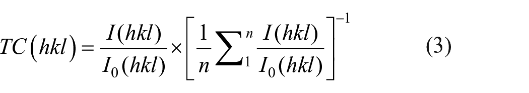
where I(hkl) is the measured intensity of a plane (hkl), Io(hkl) is the standard intensity of the plane (hkl) taken from the JCPDS data, and n is the number of diffraction peaks.
The morphologies of the films were observed using a Prisma E scanning electron microscope (SEM) operating at a voltage of 15 kV equipped with energy-dispersive X-ray spectroscopy (EDX) composition analysis. A Shimadzu 1800 UV/Visible scanning spectrophotometer was used to study the optical properties of the thin films. The optical transmittance values were collected in the range of 300 to 800 nm with a scan of 1 nm. The samples resistance was measured, in dark and at room temperature using a four-probe technique.
Results and discussion
In spin coating method, the films’ thickness can be controlled by various parameters including the spinning rotation, the solution concentration, and the solution viscosity. Here, we studied the variation of the film’s thickness as a function of the salt concentration at a spinning speed of 3000 r/min (Figure 2). As can be deduced, the thickness of the as-prepared films increases almost linearly with the solution concentration according to the following empirical law


Variation of film thickness as a function of the solution concentration.
Structural properties
The XRD patterns of the as-synthesized samples, obtained with different precursor’s molarity (0.1M; 0.15M; 0.2M, and 0.25M) revealed polycrystalline and pure SnO2 thin films (Figure 3). All patterns are composed of several peaks originating from the diffraction plans (110), (101), (200), (111), (211), (220), (002), (310), and (112) assigned to SnO2 tetragonal rutile structure (JCPDS card no. 01-0657). There are no extra peaks assigned to any secondary phase indicating the purity of the synthesized films. The XRD patterns were analyzed in order to determine the lattice parameters such as the dhkl interspace plans, and the cell parameters a, b, and c. The crystallite sizes were calculated using the Debye Scheerer and Hall–Williamson analysis to determine the crystallite along with the strain in the film network. The calculated lattices parameters values obtained for different samples are regrouped in the Table 1. The values of crystallite size estimated using both methods are slightly different, they vary from 4.5 to 7 nm. Larger crystallite size is measured for the film prepared at the medium concentration of 0.15M. Similar crystallite size in the order of 7 nm are reported by Shaban et al. 22

XRD patterns of SnO2 films at different concentrations (a) 0.1M, (b) 0.15M, (c) 0.2M, and (d) 0.25M.
Lattice parameters a, b, c, lattice spacing dhkl, Dsh crystallite size calculated using Debye Scherrer; DW-H crystallite size calculated using Hall–Williamson and strain in film network.

As seen in Figure 4, the lattice parameters a and b have values ranged from 4.701 to 4.761 Å, which are within their values in the bulk material (ao, bo = 4.737 Å). While the c values are ranged from 3.159 to 3.231 Å, the c values calculated in the whole samples are lower than its value in the bulk material (co = 3.816 Å). From this, one can conclude that the elementary cell is compressed along the c direction normal to the substrate. This is consistent with the negative slope Hall–Williamson plot of βcosθ as a function of 4sinθ as shown in Figure 5.
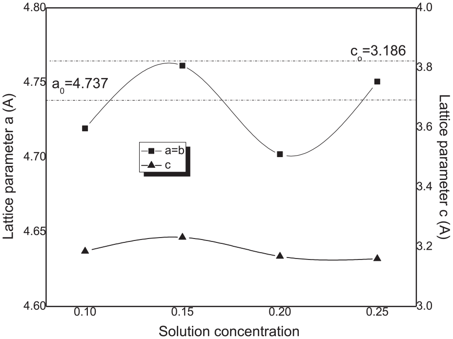
Variation of lattice parameters a, b, and c as a function of solution concentration used for films deposition.

Examples of Hall–Williamson plot used for the estimation of the crystallite size and strain in films network for film prepared with molarity of (a) 0.15M and (b) 0.2M.
The variation of the crystallite size and strain in the film network estimated using H-M calculation, are shown in Figure 6. The film prepared at the moderate concentration of 0.15M has the larger crystallite size and the lowest strain. The strain in the film network varies oppositely to the crystallite size. Obviously, during film growth, the stress and strain can be relaxed by increasing the crystallite size through the atoms ripening and atoms rearrangement. 28 Lower crystallite size means a larger number of crystallites and larger strain due to the pressure between different crystallites.

Variation of the crystallite size and strain estimated from Hall–Williamson analysis as a function of the solution concentration.
To have an insight on the quantitative information concerning preferential orientation of different diffraction planes we have calculated the texturation coefficient of the three intense peaks that is (110), (101), and (211) and shown in Figure 7. It is worth noting that a sample with randomly oriented crystallites has a TC(hkl) = 1, for all peaks, the larger this value, the larger the number of crystallites oriented in the (hkl) direction. As can be deduced from this figure, the influence of the solution concentration upon the preferential orientation can be divided in three regions: (1) low concentration (equal to 0.1M), (2) medium range (0.15–0.2M), and (3) relatively larger concentration (0.25M). The films prepared at low concentration (1) and higher concentration (3), do not exhibit any preferential orientation; the three planes have almost the same texturation coefficient with a slight preferential along the direction (101). However, at medium solution concentration (M = 0.15), the direction (110) is the preferential one.

The texturation coefficient of three diffraction peaks variation with the solution concentration.
Several authors have observed the same preferential orientation in SnO2 thin film prepared by sol gel method.21,29,30
From the variation of the crystallite size, strain, and texturation coefficient, we suggest that at both low and high concentrations, film growth is achieved along the whole directions, resulting therefore in lower crystallite size and larger strain. While at medium solution concentration, the growth becomes preferential along the (101) direction leading to larger crystallite size and consequently lower strain.
Morphological properties
Top-view SEM images of the prepared SnO2 thin films with different solution concentrations are shown in Figure 8. The obtained films are dense, homogeneous, and continuous, with uniform and smooth surface.

SEM images of the different SnO2 thin films prepared with various solution concentration (a) 0.1M, (b) 0.15M, (c) 0.2M, and (d) 0.25M.
Similar images have been reported by Kwoka et al. 31 Grains start appearing and larger crystallite sizes in the range of 14 to 17 nm are formed after annealing above 400 °C32,33 or when films are deposited at high substrate temperature in the case of SnO2 thin films prepared by spray pyrolysis. 30
In Figure 9, we have reported the EDX spectra of the prepared SnO2 films with various salt molarities. It is evident from these spectra that the presence of the two required Sn and O elements constituting the film. The small Si peak is originating from the used glass substrate. In Table 2, we have reported the variation of Sn, O atom and the O/Sn ratio. As shown in the table, the O/Sn varies in the range from 2.3 to 1.28. From these results, one can conclude that the films prepared at low molarities, 0.1M and 0.15M, have better stoichiometry. In addition, by increasing the molarity of the film’s preparation, the film became more oxygen deficient. It worth noting that the oxygen defect may behave as donor impurity by creating a shallow SnO2 energy band diagram. Correspondingly, this oxygen deficiency may improve the film conductivity.

EDX spectra recorded in the SnO2 thin films prepared at various salt molarities (a) 0.1M, (b) 0.15M, (c) 0.2M, and (d) 0.25M.
Atomic composition and the O/Sn ration measured in films prepared with various molarities.

Optical properties
The optical properties of the as-prepared tin oxide films were studied in the spectral range of 300–800 nm. The transmittance spectra show that all films are transparent in the visible region, where the maximum transmittance is about 98% for film prepared at low concentration. The transmittance decreases with increasing salt concentration. This reduction is attributed to the film thickness increases as shown in Figure 10. Moreover, the transmittance of the whole films exhibits interference fringes in the visible range; this is a confirmation of the film smoothness, a surface uniformity as deduced from the SEM observations (Figure 8).
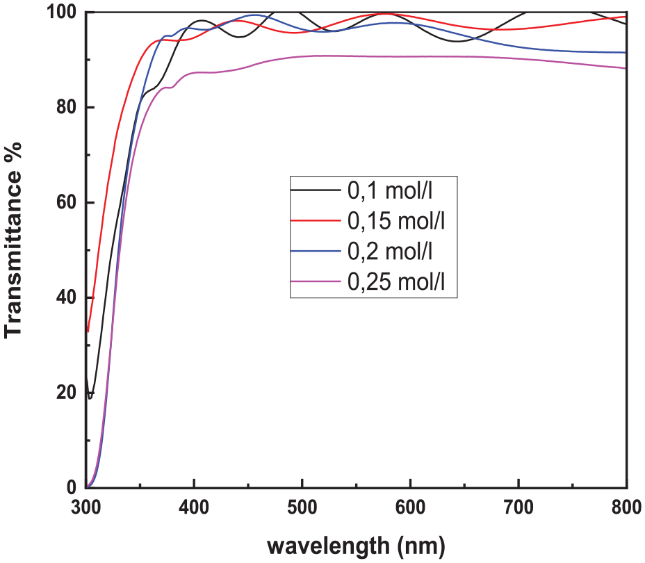
Optical transmission of SnO2 films prepared with different concentrations.
Film transmittances are used for the films band gap calculation. Since SnO2 is a direct band gap semiconductor transition, the optical band gap energy of film was determined using the following equation 34
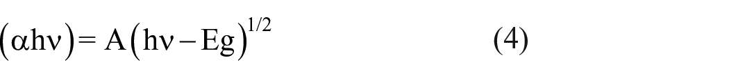
where α and hν are optical absorption coefficient and incident photon energy, respectively.
The band gap is estimated from the slope intercept with the x axis of the Tauc plot (αhν) 2 as function of photon energy hν. The transmittance spectra are also exploited to calculate the disorder in the film network. The latter is characterized by the so-called Urbach tail or Urbach energy Eoo. It is worth noting that the structural defects due the deviation of the band length or angle from their standard values in the bulk cause the appearance of electronics defect at the band edge, forming a band tail; the width of this band tail is the Urbach 35 energy. In the sub-band gap region, the absorption coefficient varies according to the following expression 35

where Eoo is the Urbach energy.
The slope of the graph ln α = f (hυ) is used to estimate the band tail width quantifying thereafter, disorder in the film network.
In Figure 11, we have reported in the same graph both the band gap and the band tail width. The band gap is reduced from 3.9 to 3.8 eV with increasing salt concentration. As can be deduced from Figure 10, the band gap and the Urbach tail behave oppositely with the salt concentration variation. As depicted in insert Figure 11, showing a semiconductor band structure, any increase in the band tail width is accompanied by the band gap reduction. Then, this may explain that the bang gap variation is controlled by the disorder in the film network.
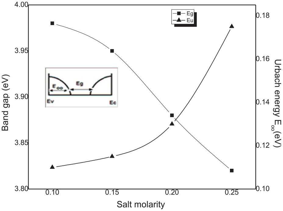
Variation of the optical band gap and disorder in film network as a function of the molar concentration. Insert band diagram showing the correlation between the band gap and the Urbach tail.
The calculated band gap is larger than the SnO2 bulk value of 3.6 eV. Due to the small crystallite size measured in our samples, the large value in the optical band gap is attributable to the quantum size effect. 36 Similar band gap values for spin-coated SnO2 thin films are reported in the literature.37,38
Electrical properties
The electrical resistivity of the films was measured using the four-probe method at room temperature. The measurement is realized by making four ohmic electrical contacts on the sample surface. The electrical conductivity data of SnO2 thin films with different molar concentrations are shown in Figure 11 along with the band gap. The observed enhancement in the conductivity of SnO2 film with the solution molarity may originate from the band gap reduction. The latter causes the increase in the free carrier concentration in the conduction band of SnO2, leading, thereafter, to the increase in the electrical conductivity of the films. Moreover, the increase in the disorder in the film network as shown in Figure 12 might be at the origin of the conductivity improvement beside the oxygen reduction as deduced from EDX analysis. It is worth noting that structural defect and oxygen vacancy can be considered as a doping defect by creating a donor level close to the conduction band, 39 yielding thereafter to the increase in the free carrier in the conduction band.
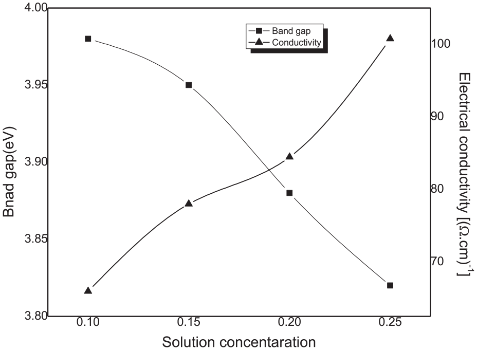
Variation of the electrical conductivity and the band gap of SnO2 thin films as a function of the solution concentration.
Transparent conducting oxide (TCO) films, such as SnO2, are commonly used as front contact material in solar cells. This application requires films to have both high transparency and high conductivity. Thereafter, in order to ascertain the effectiveness of these TCOs as a front contact, the figure of merit parameter is introduced. The figure of merit is defined as the product of the transparency and conductivity, and it can be calculated using Haacke formula 40 expressed as

where T is the transmittance and Rsh is the sample sheet resistance.
The figure of merit of different samples is calculated using the mean value of transmittance at the visible wavelength of 600 nm. The sheet resistance Rsh is measured by the four-probe technique. Table 3 shows the regrouped obtained figure of merit in the prepared SnO2 thin films. According to this finding, the solution concentration slightly affects the spin-coated SnO2 thin films; nevertheless, increasing the solution concentration reduces the film’s figure of merit. This is due to the reduction in the film transmittance, according to relation (6), and the transmittance has a dominant effect in comparison to the electrical conductivity.
Transmittance, conductivity, sheet resistance, and figure of merit measured in different SnO2 samples.

For comparison, we have collected some values of figure of SnO2 published by different authors (shown in Table 4). Regarding the published values, our prepared SnO2 thin film can be a serious candidate as TCO top electrode for the optoelectronic applications.
A comparative table of different values of figure of merit reported by different authors.

Conclusion
In the present work, undoped SnO2 thin films have been successfully synthesized by spin coating technique. The effect of the concentration of the salt precursor was investigated. The XRD analysis revealed the formation of nanocrystalline SnO2 rutile phase. The (110) preferential orientation was observed only when using a moderate concentration, that is, 0.15M, while the other salt concentrations favor the growth along the all directions. The crystallite sizes are less influenced by the solution concentration. SEM observations reveal the formation of smooth and continuous films morphology. The obtained films have a high transparency in the UV-Vis range, the recorded transparency is ranged from 90% to 97%, and a wide band gaps in the range of 3.6 to 3.9 eV. The measured film’s electrical conductivity, at ambient temperature, is ranged from 66 to 100 (Ω.cm)–1. The figure of merit of the prepared SnO2 thin films reaches the value of 9.8 × 10⁻³. Overall, from the optical and electrical characterization, we guess that the synthesized SnO2 thin films can be a serious candidate as transparent electrodes in optoelectronic applications.
Footnotes
Data availability statement
Data will be made available on request.
Declaration of conflicting interests
The author(s) declared no potential conflicts of interest with respect to the research, authorship, and/or publication of this article.
Funding
The author(s) received no financial support for the research, authorship, and/or publication of this article.