
Abstract
The use of natural silk nanofibers (SNFs) in flexible materials has been widely studied in recent years. However, the reported preparation methods are not suitable for commercial consideration. We report a method for rapid preparation of silk nanofibers in water. Silk nanofibers were mixed with graphene to prepare composite conductive silk films (CSF) with good flexibility and conductivity. Micro-morphology shows that graphene is embedded and modified between silk nanofibers to form a stable structure. Infrared analysis showed that graphene compounds do not alter silk formation, especially in the stable silk structure. Resistance tests show that the process is most effective when the ratio of SNFs to graphene is 1:3. This study offers a new approach to fabricating bioelectric devices.
Introduction
With the growing demand for smart wearable devices, environmentally friendliness and compatibility are important considerations. Due to wear and tear, the continued use of traditional synthetic materials is limited.
Silk, as a natural fiber, has excellent mechanical properties and good compatibility,1,2 but still has some flaws such as poor electrical conductivity. By combining silk with other materials, the functional impairment of silk materials can be improved, and functional compounds with good biocom-patibility and electrical conductivity have received much attention and extensive research in recent years. Graphene is a slow-moving material and has a wide range of application in the field of flexible materials. To date, research has been concerned with the combination of graphene and silk by graphene materials to reinforce silk physically and chemically. Here, graphene is mixed with a silk fibroin solution and applied to the skin to form a pattern, which can respond to changes in the external environment. Studying the composite sensor of graphene silk fibroin is very important and promising for the design of epidermal electronics.3-10 A graphene/silk fibroin (SF) suspension system with good dispersion and high stability was developed, and many types of materials such as film, fiber, and coating were produced. The available materials retain the electronic advantage of graphene.
Silk has a natural structure in the high-end category, and silk nanofibers are usually prepared through either “top-down” or “bottom-up” processes. 11 The “bottom-up” approach is to remove fibroin silk and reassemble it into fibers. This is a common method for assembly and electrospinning.
While nanofibers are being created, this process destroys the natural structure of the silk.12,13 “Top-down” processing separates the perfect silk by exploitation. The most widely used methods are ultrasound, hexafluoroisopropanol, ionic liquid, and formic acid-Ca2+ silk treatment system.8,14 Although these methods prevent structural losses, there are still some problems, such as overuse of energy, residues of harmful substances, and low yields.
In this paper, we explore how to make nanofiber silk and blend it with graphene to make a silk-based film, which not only retain silk properties but also electric properties. Such matial can be widely used in the field of textiles, clothing, bodyuilding, and optoelectronic equpment.
Materials and Methods
Preparation of Silk Nanofibers
Bombyx mori (B. mori) silk was boiled three times in 0.06% (w /v) Na2CO3 solution for 30 min to remove sericin. The degummed silk was washed completely with distilled water and placed in an oven at 60 °C for 24 h. The treated silk was soaked in ternary solution (CaCl2:CH3CH2OH: H2O=1:2:8 molar ratio, with the bath ratio of 1:250) and treated at 60 °C for 6 h. The mixture of silk and the ternary solution was mechanically sheared for 10 min, 15 min, 20 min, and 25 min Silk of different diameters were obtained, then washed and dried completely for further use and characterization. The SNFs were fabricated by the established procedure shown in Fig. 1A.
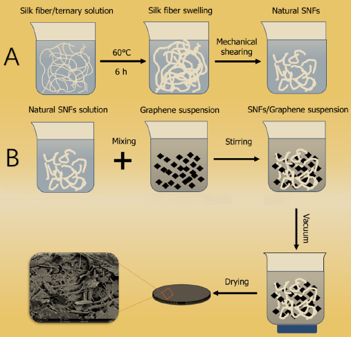
Schematic diagram of the manufacturing process for SNFs (A) and CSF (B).
Preparation of Composite Conductive Silk Films (CSF)
A uniform SNF aqueous dispersion system (0.25%, w/v) was mixed with graphene suspension (0.25 wt%) with solute weight ratio of 1:0.5, 1:1, 1:1.5, 1:2, 1:2.5, and 1:3 via tip-assisted sonication (at 300 W) for 10 min and 20 min to obtain the dispersion system. The obtained dispersion system was filtered in a vacuum on the PTFE membrane (0.22 μm pore size). After drying and separating the base membrane, the composite conductive silk films (CSF) were obtained (Fig. 1B).
Morphology of SNF Film and CSF
Drip silk fibers with different shearing time on the glass slide and diameter changes as a result of shearing time was observed by optical microscope (XSP-2C, China). To observe the surface morphology of the sample, the sample was cut into small pieces and affixed to the scanning electron microscope sample table. The diameter analysis was performed with a scanning electron microscope (SEM, Zeiss, EVO MA 10/LS 10, Germany).
Structure Analysis of CSF
Fourier transform infrared spectroscopy (FTIR) spectra of the samples were obtained using a Bruker spectrometer (VERTEX 70, Germany) in the spectral region of 400-4000 cm−1, to characterize the silk nanofiber/graphene composite in the CSF.
Electrical Properties Measurements
The resistance (Ω) of CSF cut into 10 × 20 mm rectangles was measured by a four-probe electric meter (KDB-1, Guangzhou, China). The statistical resistance is the average value of the product obtained after at least five measurements at different positions on the surface.
Results and Discussion
Morphology of SNF
After swelling treatment and mechanical shearing, the diameter of silk fiber changes greatly, and most of the silk split into micron fiber and nanofiber (Fig. 2A-D). According to Fig. 2E-H, when the shearing time is 10 min, 15 min, 20 min, and 25 min, the diameter of the fiber decreases from 10 μm to 5 μm, then to 1 μm, and finally reaches the nanometer level. With the increase of mechanical shearing time, the intertwining among fibers becomes less, the distribution of fibers in the system is more uniform, and the size decreases, which almost reaches the nanometer level after 25 min. The fiber formed by stirring for 25 min was selected as the raw material of the conductive film because it had less entanglement, better dispersion, smaller fiber size, and more uniform distribution. The silk nanofibers prepared by mechanical shear have good stability and high yield, so they are suitable for mass production.
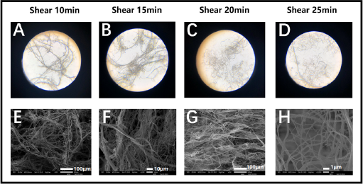
Morphology of silk fiber with various mechanical shearing time viewed under optical microscope (A-D) and scanning electron microscope (E-H).
Morphology of CSF
The morphologies of SNFs and CSF were observed by a scanning electron microscope (Fig. 3). The SNF films with micropores on the surface can be obtained by selecting SNF with suitable shearing time. The graphene on the surface of CSF is uniformly distributed and wound with silk nanofibers. Graphene covers the micropores formed by the intertwining of nanofibers. With the increase of graphene concentration, the exposed silk nanofibers on the film surface decrease and this structure helps to improve the electrical conductivity of CSF.
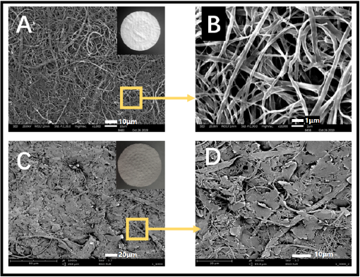
Surface morphologies of SNFs (A, B) and CSF (C, D) were characterized by scanning electron microscope.
Structure Analysis of CSF
FTIR analysis (Fig. 4) showed that graphene was successfully compounded into the material. Graphene showed some unique characteristic bands but did not change the characteristic bands of silk. For example, 1625 cm−1 (amide I) and 1515 cm−1 (amide II) show that CSF has a stable β-sheet structure.
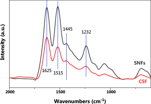
FTIR structure analysis of SNFs and CSF.
Electric Behaviors of CSF
From Fig. 5, the surface resistance of curves A and B decreases with the increase of the graphene ratio. For the conductive film with the same graphene concentration, the surface resistance of A is always greater than that of B. When the concentration of graphene is constant, the longer the ultrasonic time, the smaller the resistance. This is because longer ultrasonic mix time of graphene/silk nanofiber produces a better composite of graphene and silk nanofiber and less graphene is lost. When the ultrasonic time remains the same, higher concentration of graphene leads to smaller resistance of CSF. The lower resistance (higher conductivity) of CSF is due to an increase in the amount of graphene adsorbed. With the increase of the ratio of graphene, the resistance of conductive silk fibroin film begins to decrease rapidly. When the ratio of SNF to graphene is 1:2.5, the resistance decreases obviously, because the surface area of silk nanofiber is limited. The amount of graphene that can be absorbed is also limited when the ratio of SNF to graphene is 1:3, the adsorption capacity has approached the saturated state, and it is of little significance to increase the concentration of graphene.
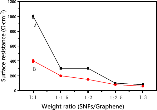
Surface resistance of CSF at various weight ratios for 10-min tip-assisted sonication (A) and 20-min tip-assisted sonication (B).
Conclusions
In this study, we reported a physical method for the preparation of silk nanofibers, which can be used to prepare silk nanofibers in large quantities, and it has all the characteristics of environmental-friendliness and high efficiency. The silk nanofiber was successfully prepared. Based on the good dispersion of silk nanofibers, we use the water system to mix silk nanofibers with graphene, and successfully prepare CSF, with excellent electrical conductivity by vacuum filtration. The composite of SNFs and graphene is formed, and the CSF is stable. This method can simplify large-scale production. This kind of material provides a new idea for the preparation of bioelectric materials.