
Abstract
This study applies a two-dimensional discrete wavelet transform (2D-DWT) analysis using a biorthogonal filter, followed by a continuous analysis employing an anisotropic Cauchy wavelet, on electroluminescence (EL) images of polycrystalline and monocrystalline silicon photovoltaic (PV) cells under varying current levels. The wavelet-based approach facilitates the identification of electrode-cell interfaces defects that are not readily visible in EL imaging alone. Our findings reveal that cells with poor soldering at electrode interfaces exhibit up to a 16.3% reduction in maximum normalized power (MNP), directly correlating with reduced current density across certain busbars. The quantitative improvements in defect detection underscore the method's efficacy in addressing power inconsistencies tied to internal PV cell failures. This technique shows promise as a non-invasive diagnostic tool for assessing PV cell performance and structural integrity.
Introduction
Driven by the urgent need to address climate change and meet the rising global energy demand, many nations have committed to a sustainable energy transition to achieve carbon neutrality by 2060. Renewable energy sources, particularly solar power, play a crucial role in this shift. However, the long-term reliability and efficiency of photovoltaic (PV) systems remain a concern due to environmental exposure and operational stresses that lead to structural and electrical failures over time (Tembo and Subramanian, 2023). For this reason, several technologies, such as hydroelectric, wind, solar, and biomass have been investigated to replace fossil fuels as a sustainable and clean energy production alternative. In this sense, solar energy has been developed exponentially thanks to technological innovation and research activities in recent decades. Countries such as the United States through the Solar Energy Technology Office (SETO), member states of the E.U., in addition to Norway and Turkey or Asian Countries, have invested in PV technology development (Pezzutto et al., 2021). In line with Gorjian et al., the policies outlined in the 6th development plan had a negative impact on Iran's solar PV deployment (Gorjian et al., 2019). Similarly, the increase in solar PV adoption in the Philippines is credited to ample solar irradiation and supportive governmental policies (Farias-Rocha et al., 2019). Analyzing various policies, Raina and Sinha found that the Jawaharlal Nehru National Solar Mission (JNNSM) has played a significant role in bolstering India's solar PV capacity (Raina and Sinha, 2019).
Currently, PV technology is dominated by crystalline silicon (c-Si) cells due to their high stability, low cost, and efficiency. According to data provided by the International Technology Roadmap for Photovoltaics (ITRPV), PV technologies based on c-Si generated ∼ 95% of the total 135 GW installed in 2020. The remaining part is shared by PV technologies of Copper Indium Selenide (CIS), Perovskite, Cadmium Telluride (CdTe), Copper Indium Gallium Selenide (CIGS), and other materials (Sun et al., 2022; Dávila-Pulido et al., 2021). However, reliability problems in the installed PV systems generate concern because they face adverse environmental and mechanical conditions during their useful life. Even during their manufacturing, they can suffer damages due to the production processes (Santhakumari and Sagar, 2019). The presence of failures and early deterioration of its components or connections during operation can generate electric arcs, short circuits, and hot spots, which increase the degradation of the components and lead to energy losses of the PV system (Pimpalkar et al., 2023). In general, some of the most recurring failures of installed PV systems are in the back sheet, corrosion of the busbar, corrosion of the connection between the band and the chain of the cell, hot spots, discoloration of the solar cell, insulation resistance, module frame distortion, interface box corrosion, frame failure corrosion, glass contamination/cracks, among others (Rajput et al., 2020; Mellit et al., 2018).
To ensure the operational reliability of PV systems, various non-destructive testing (NDT) methods have been developed, including electrical measurements, thermography, and electroluminescence (EL) imaging. EL imaging allows for the detection of both visible and invisible structural defects such as microcracks and soldering issues, which are critical to maintaining cell efficiency. However, while EL provides valuable surface-level information, it often lacks the frequency-specific detail needed to detect internal defects affecting power performance (Kasemann et al., 2008). Technological development has allowed new non-invasive methodologies such as computer vision, wavelet analysis, and artificial intelligence to detect some failures more accurately and efficiently (Waqar Akram et al., 2022). In addition, techniques based on artificial intelligence, such as automatic and supervised learning, allow increasing reliability and automation in monitoring, detecting, and diagnosing of different failures of PV and other systems (Djalab et al., 2019; Aallouche and Ouadi, 2022; Tao et al., 2020; Moradi Sizkouhi et al., 2021; Carbonó dela Rosa et al., 2023). Wavelet transform analysis, as a mathematical tool for time-frequency domain analysis, offers unique advantages over traditional Fourier and machine learning-based methods in PV diagnostics. Unlike Fourier transforms, which are limited in spatial resolution, wavelet transforms enable multi-resolution analysis, making it possible to detect high-frequency signals associated with specific defect regions. By applying two-dimensional discrete and continuous wavelet transforms (2D-DWT and 2D-CWT) to EL images, this study provides a more detailed assessment of PV cell integrity, specifically targeting defects in electrode-cell interfaces that affect current flow and power output (Ahmadipour et al., 2022; Mansouri et al., 2018).
Although methods like I-V curve analysis and infrared thermography are useful for detecting electrical and thermal anomalies, they have limits in terms of spatial resolution and the ability to discover microstructural flaws. Thermography, for example, is extremely sensitive to temperature changes, yet it could miss non-thermal flaws in solar cells. I-V analysis lacks the spatial resolution required to pinpoint specific busbar-cell interface problems, despite being thorough in describing overall cell performance. By separating out specific patterns linked to electrical contact failures, wavelet analysis, on the other hand, provides a multi-resolution method that improves fault detection capabilities by offering targeted frequency and spatial information (El-Banby et al., 2023).
Different works in the literature can be found trying to detect different defects or elements in the surface of the PV cells. The work of Saint Cast et al., (2020) is focused on finding fingers using a Fourier-based analysis using only a single image of Photoluminescence. Another proposal presents a similar approach for detecting the rear contact voids in PERC cells (Öğütman et al., 2018). Other more complex approach uses Machine Learning techniques (mostly Deep Learning) to detect various defects in the PV cells using their EL images, many of these works are based on cell level, since they segment the PV modules into all their cells. It also evident in the number of works how EL is the technique most used to take images of the PV cells (Mellit and Kalogirou, 2008; Mateo Romero et al., 2022; Mateo-Romero et al., 2024). In (Karimi et al., 2019), the authors perform a set of tests on PV modules and obtain EL images of these PV modules. The images, once processed, are used to detect typical failures in PV modules. The authors of that work do not provide I-V (Current Voltage) curves of their cells; therefore, they cannot make a comparison of their EL images with respect to the true value of power delivered.
The authors in (Karimi et al., 2020), study the relationship between the series resistance (obtained from the I-V curves of PV modules) with the EL images obtained from them Subsequently, the authors take advantage of this relationship to propose a system for estimating series resistance from EL images. The system proposed in that work is much more complex than the one proposed in this article because it provides a simpler and more automatic method. On the other hand, in (Colvin et al., 2021) the authors demonstrate the importance of good connection between PV cells within a PV module. Furthermore, the authors demonstrate that the effect on the performance of the PV module depends on the position of the fault. In this study, the authors use interconnection failures between cells, and do not focus on failures of the metallization mesh in the cell itself, whether failure due to corrosion or poor welding. The authors use three different methods to calculate the cell resistance of the PV module, but do not use artificial intelligence or Deep Learning techniques.
All the articles analyzed agree on the need to use techniques that allow the identification of problems in PV cells, to subsequently be able to draw conclusions at the PV module level. There are few articles that focus their interest on the relationship between series resistance increase problems and EL images, in this sense, our article focuses on this aspect, and through a spatial-frequency analysis is conducted through the application of the two -dimensional discrete analysis with a biorthogonal filter, this objective is achieved. With this simplicity of the process, the model allows detection of problems in series resistance, which would otherwise have gone unnoticed through conventional image treatment.
This study proposes a novel application of 2D discrete and continuous wavelet analysis on EL images of polycrystalline and monocrystalline silicon PV cells to detect electrical contact failures at the electrode-cell interface. By combining EL imaging with wavelet analysis, this research aims to identify soldering defects and other connection issues that contribute to increased series resistance and reduced power generation in PV cells. The results demonstrate that cells with compromised soldering at electrode interfaces experience up to a 16.3% reduction in normalized maximum power output. This wavelet-based approach not only improves defect detection but also provides quantitative insights into the extent of performance loss caused by specific structural issues. Such a diagnostic tool offers a non-invasive means of evaluating PV cell health and supports future integration with AI-driven fault detection systems. The following sections provide further insights into theoretical analysis, methodological considerations, conformation of the database, results, and discussion.
Theoretical analysis in the spatial-frequency domain
The frequency domain analysis aims to discern trends, discontinuities, periodicities, and phase alterations in data by transitioning from the time domain to the frequency domain. Prominent methodologies for such transformations include Fourier, wavelet, and Z power techniques (Karasu and Saraç, 2022; Azpiroz-Leehan, 2000). This spectral analysis can be extended to the spatial domain; this refers to the matrix of pixels that make up the normal domain of images (Zhao et al., 2022). The frequency transformation performed in this domain operates on the image pixels and is commonly used for edge detection, noise filtering, comprehension, and failure detection, among other applications. Frequency refers to the speed of change of color of the image pixels in the spatial domain. Therefore, high-frequency areas of the image have fast color changes, while slow-changing areas have a lower frequency. The image transformed to the domain of the frequency is conformed, with regions of high frequency like the edges and regions low frequency show a smooth pattern. As the output of this process, we obtain a transformation, not an image. To produce the image again, the inverse transformation process must be conducted (Parida and Bhoi, 2017; Jumah, 2013).
Two-dimensional wavelet analysis serves as a mathematical tool for image processing, enabling examination across various frequencies and resolution scales, a principle known as multi-resolution. In addition, provides several advantages over other techniques, such as machine learning-based image processing or standard Fourier transforms. Although machine learning methods have demonstrated excellent accuracy in defect detection, they can be computationally demanding and frequently require large datasets for effective training. On the other hand, Fourier transforms are generally limited in their ability to localize defects within specific regions due to their lack of spatial resolution. By contrast, wavelet transforms allow multi-resolution analysis, providing detailed insights at various scales and locations within the image, which is essential for accurately detecting failures at the electrode-cell interface(Wang et al., 2014; Versaci, 2021).
This analysis is achieved through the application of the 2D-DWT, which partitions the image pixels into two discrete approximation components and two detail components using high-pass and low-pass filters. In Figure 1(a), the discrete decomposition process of an image at multiple scales is illustrated, with each scale consisting of four sub-bands: the pixels representing high frequencies contribute to the coefficients of detail (cD), vertical (cDv), horizontal (cDh), and diagonal (cDd). Conversely, pixels representing low frequencies contribute to the approximation coefficients (cA), which encapsulate information about the smoothest regions of the image (Wang and Lu, 2010; Jayawardena et al., 2009). Figure 1(b) displays the coefficients of the first level of decomposition, while Figure 1(c) depicts those of the second level. This process can be iterated up to the desired level of decomposition.
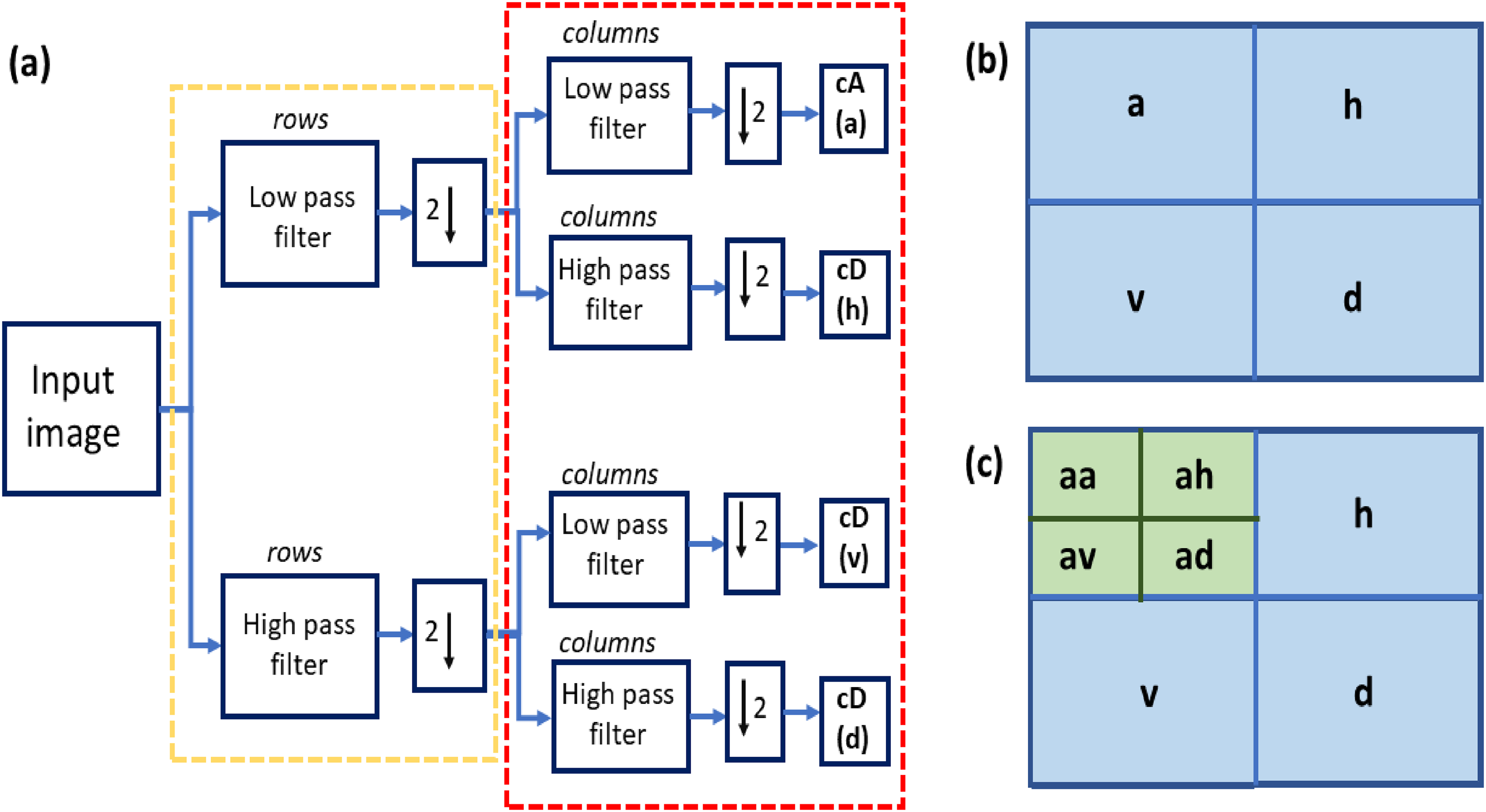
Flowchart of the basic 2D discrete wavelet decomposition process (a); first-level decomposition (b); second-level decomposition (c).
Several wavelet filters, such as Haar, Daubechies, and Symlet, have been developed for discrete image processing (Karasu and Saraç, 2022). However, we will focus on the Biorthogonal wavelet (Bior) filter, which will be used to process the electroluminescence images studied in this research work. The main characteristic of this filter is flexibility, since it is made up of two wavelets with different regularity characteristics, which allows each one to deal with different tasks in image processing (Azpiroz-Leehan, 2000). This feature enables precise adjustments for different image-processing tasks, allowing one wavelet to manage high-frequency components (detail) and the other to manage low-frequency (approximation) components. The Bior wavelet's flexibility and duality make it particularly effective for highlighting discontinuities caused by electrical contact failures between the cell and electrodes. By decomposing image data into distinct frequency bands, the Bior wavelet can separate high-frequency components, often associated with abrupt changes or potential defects (such as microcracks or soldering flaws), from low-frequency background information that represents more uniform areas without structural anomalies (Zhou et al., 2024).
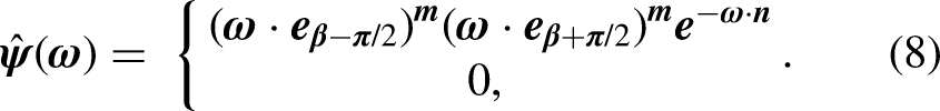
The wavelet function


The 2D CWT, as defined in Equations (4) and (5), acts as a spatial-frequency filter, allowing localized analysis across scales and orientations. This transform's ability to isolate frequency variations is crucial in detecting subtle structural anomalies in PV cells and is defined as follows (Antoine et al., 1993).


In comparison to traditional spectral analysis methods, the 2D-CWT stands out by providing localized spectral information across various scales. This is achieved by acting as a local scale and position filter on spatial domain data. The 2D-CWT excels in offering detailed spectral insights at specific positions and orientations within the data, conducting a continuous analysis across the entire spatial domain. This distinguishes it from the 2D-DWT, which generates a condensed representation of the analyzed dataset (Jayawardena et al., 2009).
Different wavelets are proposed in the literature, and some can be real, complex, isotropic, anisotropic, etc. (Antoine and Murenzi, 1996; Wu et al., 2011). In this sense, if the wavelet is isotropic, there is no dependence on the angle
Materials and methods
This section presents the methodological proposal for the analysis of the EL images polycrystalline silicon PV cells under different current values, the considerations for the conformation of the databases and the materials used to obtain the EL images and the estimation of the maximum power point for each image.
Methodology
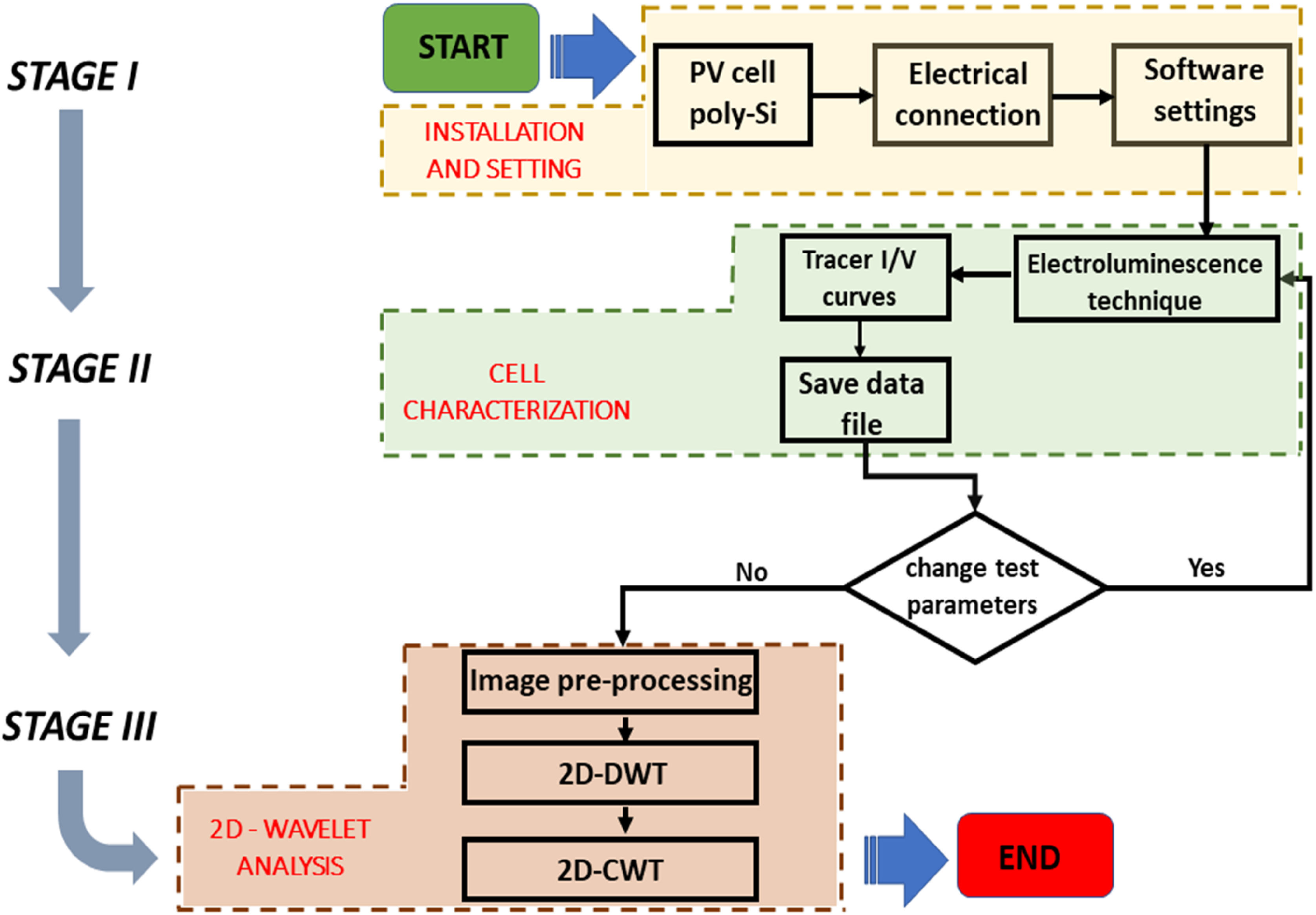
We performed a spatial-frequency analysis on electroluminescence (EL) images of polycrystalline and monocrystalline silicon PV cells, using 2D-DWT and 2D-CWT to identify connection failures between the cell and its electrodes. The methodology was organized into several stages (see Figure 2). The first stage involved setting up and calibrating the hardware and software used in the tests.
Flowchart of the methodology implemented for the spatial-frequency analysis of EL images.
In the second stage, we characterized the polycrystalline and monocrystalline silicon PV cells using electroluminescence imaging. Then, the maximum power point (MPP) is extracted and normalized, and the data is stored (Morales-Aragonés et al., 2022). The EL images are then preprocessed through filtering and edge trimming to obtain a color histogram. Subsequently, two-dimensional discrete and continuous wavelet analysis is performed, see Figure 2.
Normalization enables performance comparison across analyzed cells. We started by dividing the database into six groups based on the current used during irradiation for I-V measurements of the PV cells (3.75A, 4.5A, 5.25A 6A, 6.75A and 7.5A). It proceeds as follows:
For each group, we calculated the mean and standard deviation of the maximum power point. We applied Z-score normalization using each group's mean and standard deviation. Then, we performed min-max normalization for each group, resulting in power values normalized to a range of [0-1] with a mean of 0.5.
Figure 3 shows the 2D-CWT analysis, performed through the Matlab wavelet analyzer application, as described below. The process begins by loading the image of EL. Subsequently, the colormap is switched from grayscale to jet. A biorthogonal wavelet filter, specifically the Bior - 4.4, was chosen for the analysis. The image is then assigned a decomposition level of two. Following this, a discrete wavelet analysis is performed in 2D on the EL images. Finally, the analysis focuses on extracting and analyzing the second-level vertical detail coefficients derived from the decomposition process.

CWT analysis in Matlab of an EL image: (a) original image with ‘jet’ colormap; (b) processed image; (c) second-level vertical detail coefficients; (d) general wavelet decomposition into two levels. Source: Matlab.
A complementary analysis was performed using the 2D-CWT on the same EL image. This continuous analysis provides detailed information at various scales and spatial orientations, offering an advantage over the 2D -DWT, see Figure 4. This approach allows for a more thorough examination of the EL image transformation. For the 2D-CWT application, we repeated the first two steps of the previous process, beginning with the selection of the Cauchy mother wavelet. The angle and scale parameters were kept at their default values. The analysis then proceeded with a 2D-CWT, where the scale index was set to two, and the angle index was set to five (180 degrees). Given the complexity of the selected mother wavelet, only the modulus component was extracted for further analysis.

2D-CWT of an EL image using the Cauchy mother wavelet: (a) original image with jet colormap; (b) wavelet modulus; (c) real part of the wavelet; (d) imaginary part; (e) angle. Source: Matlab.
Materials and experimental setup for EL images (a) and materials and setup to measure and plot I-V curves for calculating MPP (b).
Materials
For the EL test carried out in the laboratory, the following materials were used: a 20A power supply, cabling, poly-Si cells, camera, camera controller hardware, PC, camera controller software and a box with an internal coating black, which seeks to keep the cell in the greatest possible darkness during the capture of the EL image (See Figure 6(a)). On the other hand, for the artificial irradiance test to measure the electrical variables, voltage-current and plot the I-V curves, the following were necessary: two 20 A power supplies, wiring, an infrared led arrangement, a fan for cooling, poly-Si cells, a three-quadrant I-V curve tracer, PC, data processing software and a box with an internal reflective coating, so that the infrared irradiance of the LED array reaches the entire surface of the cell (See Figure 6(b)).
El images of monocrystalline and polycrystalline silicon cells under different current levels: 5.25A (a); 3.75A (b); 4.5A (c) and 7.5A (d).
Images database
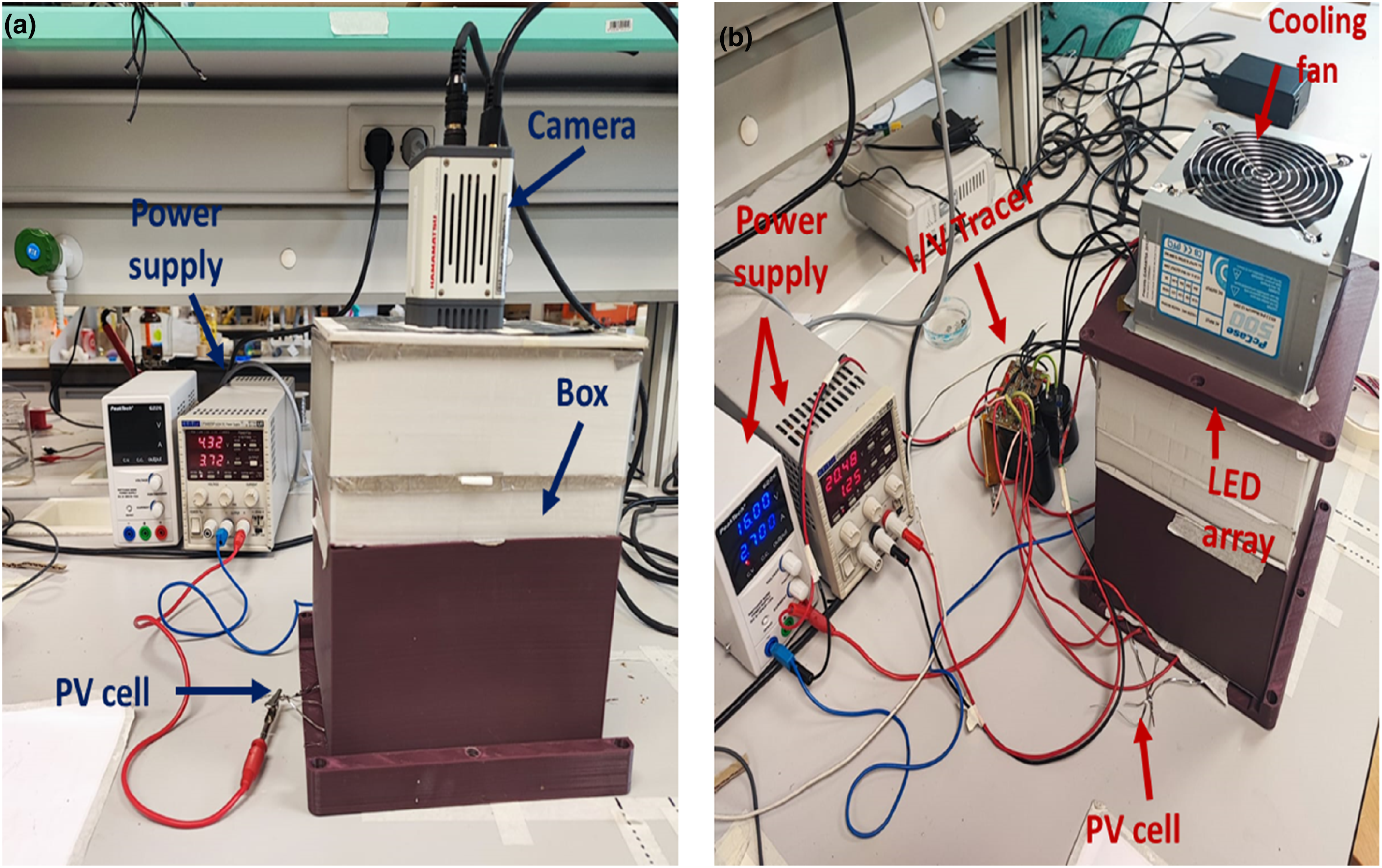
The electroluminescence (EL) images in this study were collected under controlled ambient conditions at room temperature, which minimizes variations in thermal behavior that could affect defect visibility. A high-resolution InGaAs camera was employed for EL imaging, this choice of equipment provides an elevated level of sensitivity to near-infrared wavelengths, which is essential for detecting fine-scale defects in PV cells. In addition, before imaging, the samples were carefully prepared to ensure surface cleanliness and uniformity, which reduces noise in the EL images and enhances the accuracy of the defect detection process. After the previous preparation of the cells a comprehensive dataset of 944 images has been developed, encompassing both polycrystalline and monocrystalline PV cells. The measurements have been performed at several values of current: 3.75 A, 4.5 A, 5.25 A 6 A, 6.75 A and 7.5 A, Additionally, three CSV files are provided, containing real and normalized maximum power point data for each analyzed cell (Romero, 2023).
Figure 6 shows the EL images of different mono and polycrystalline silicon PV cells after injecting a current of 5.25 A a), 3.75 A b), 4.5 A c) and 7.5 A d), respectively. EL imaging allows detection of cracks, micro-cracks in cells, as can be clearly observed in Figure 6(c). Furthermore, the El images in combination with image processing methods can help to detect energy losses, associated with a low current density flowing through the cell.
Types and causes of failures in electrode-cell interface
The electrode-cell interface in solar cells is susceptible to certain kinds of failures that can have a major effect on cell performance. A decrease in overall efficiency and an increase in series resistance can result from two common failure modes: corrosion and soldering flaws. Usually brought on by exposure to environmental pollutants or humidity, corrosion gradually erodes the conductive channels, decreasing the effective current flow. In addition to decreasing electrical conductivity, this deterioration may cause localized heating and additional structural damage if exposed for a prolonged amount of time (Saleh et al., 2022).
Soldering defects, on the other hand, are often the result of manufacturing imperfections. Inadequate solder joints between the electrode and the cell produce high-resistance spots that impede current passage and result in an unequal distribution of electrical loads. “Hot spots,” where localized heating may hasten material wear and raise the chance of failure, might result from this uneven current distribution. Although corrosion and soldering problems are particularly difficult to see with the naked eye, they can be successfully detected by highlighting minute variations in current density at the electrode-cell interface using high-resolution spatial-frequency analysis, such as two-dimensional wavelet transforms (Chang et al., 2014).
Results and discussion
Upon creating the dataset comprising Electroluminescence (EL) images and I-V curves, a notable observation was made. Certain cells exhibited lower surface illumination, and a reduced maximum power point compared to other cells of the same manufacturer and model, all evaluated under identical conditions. To investigate these discrepancies, an analysis was proposed to uncover the root cause behind the variations in surface illumination and peak cell power. The dataset includes various EL images and corresponding I-V curves, and below, you will find a selection of these images and curves that contribute to the dataset.
In comparison to other methodologies for detecting PV cell defects, the two-dimensional wavelet transform applied in this study offers distinct advantages, particularly in spatial resolution and sensitivity to defect orientation. To improve fault detection in EL pictures of PV cells, previous research has investigated several strategies, including artificial data generation and machine learning algorithms. To overcome the problem of a lack of real-world data which is essential for developing strong AI models that can identify degradation trends in PV cells a recent study, for example, used Generative Adversarial Networks (GANs) to create synthetic EL datasets. Nevertheless, these models frequently need large datasets and processing power, which may restrict their use in environments with limited resources (Romero et al., 2023). Another method, wang et al. proposed a deep learning-based technique using hybrid ResNet152-Xception architecture to tackle defect detection in PV cells. While effective, such deep learning models require substantial training data and computational resources to achieve high accuracy, as noted in their study's 96.17% binary classification accuracy on large EL datasets. However, our wavelet-based approach offers a computationally efficient alternative that enables multi-resolution analysis, which directly isolates defect-related frequency bands without the extensive data and computational demands typical in deep learning frameworks (Wang et al., 2023).
Images of EL
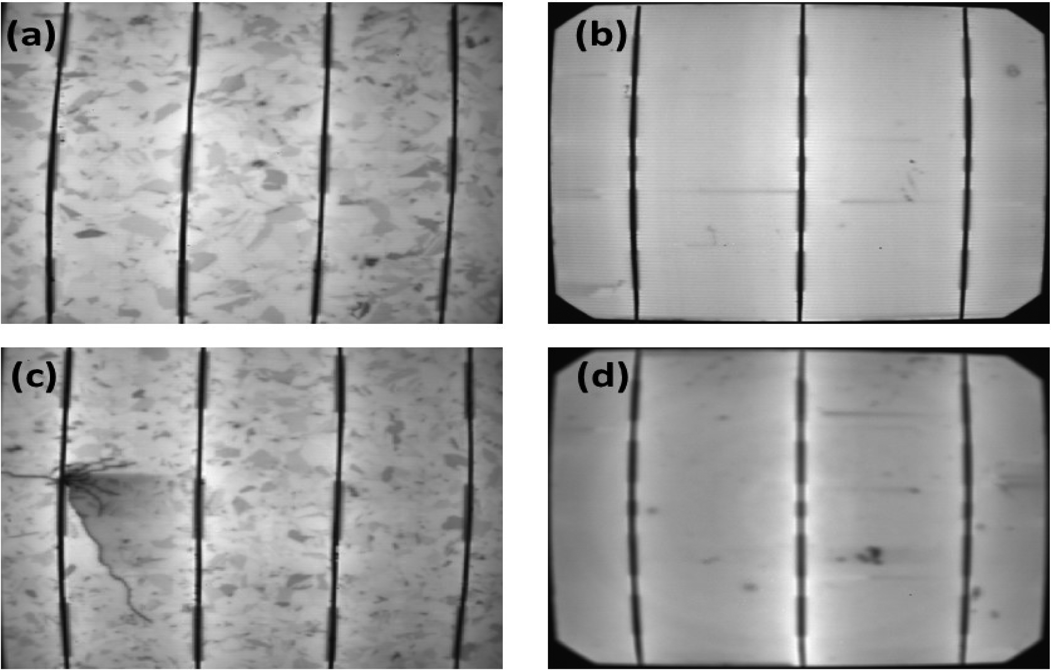
From EL imaging it is possible to detect fractures, especially microcracks and some surface defects of the cell that cannot be seen by a simple visual inspection. However, some failures that affect cell performance cannot be directly identified from EL images. For example, in Figure 7(a) is shown in one of the analyzed polycrystalline silicon cells, named PS1. Here, the EL image, non-structural damage is observed on the surface of the cell. Furthermore, this cell had a maximum normalized power of 0.92. The other polycrystalline silicon cell, named PS2, was evaluated under the same conditions as the PS1 cell (current to 3.75 A), the EL image neither is observed a superficial damage, see Figure 7(b). However, PS2 cell generated a maximum normalized power of 0.77, which is 16.3% less than in PS1 cell. Both EL images are like each other and neither detect flaws or damage on the surface of the analyzed cells.
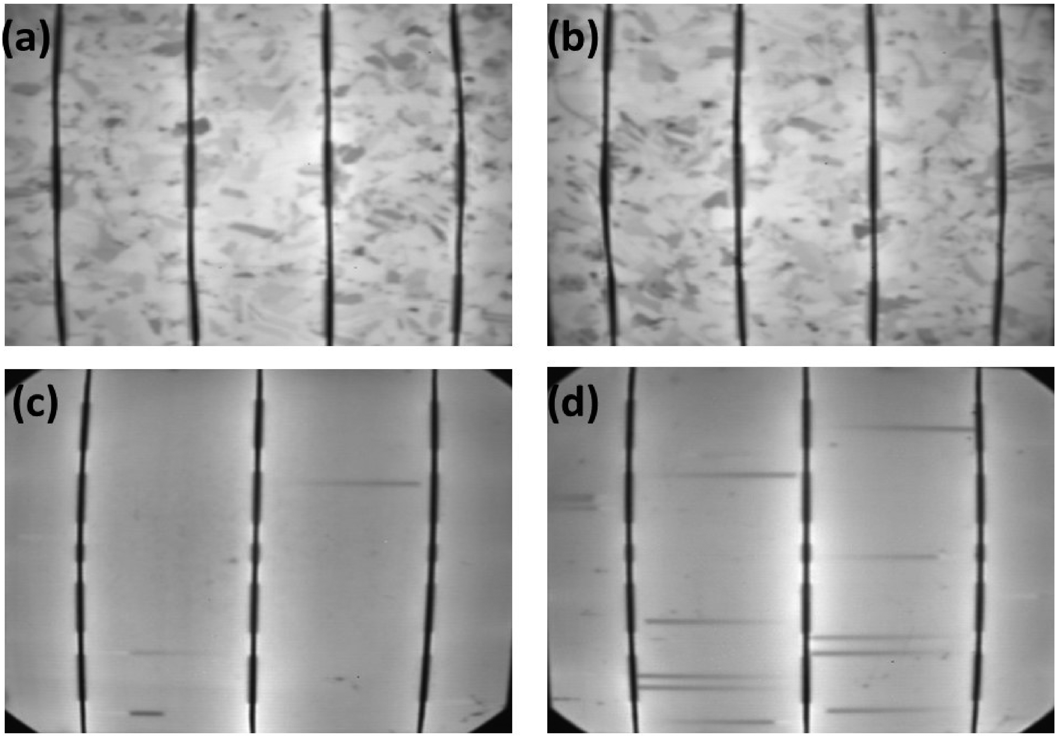
EL image of four different crystalline silicon cells, PS1 (a), PS2 (b), MS1 (c) and MS2 (d).
A similar situation was identified in monocrystalline silicon cells denoted MS1 and MS2. Figures 7(c) and (d) show electroluminescence (EL) images taken at a current of 4.5 A with no observable structural damage. However, maximum normalized power of MS1 is higher than MS2 and both cells were evaluated under the same test conditions. This decrease in the power generated by the cell with increasing irradiance indicates a problem in the current flow that limits the efficiency of the analyzed cell, and from the EL images, the root cause cannot be identified.
I-V curves
In a complementary analysis to the EL images obtained from the analyzed cells, I-V data were taken for each cell at different irradiance values, which was obtained by varying the current in 250 mA steps between [1.27A - 2.53A] from an LED array located above the PV cell as shown in Figure 5(b). The I-V curve of the PS1 cell obtained under conditions of minimum irradiance (C = 1.27A) is shown in Figure 8(a). The maximum power point (MPP) calculated from this curve is 1.36 W equivalent to a maximum normalized power (MNP) of 0.92, Figure 8(b) shows the I-V curve of the PS2 cell under the same test conditions. However, the MPP calculated in this curve is 1.22 W which represents a decrease in efficiency of 10.29% with respect to the MPP calculated for PS1 and the value of the MNP for PS2 is 0.77.

I-V curve of PS1 cell applying minimum irradiance (1.27 A) (a), PS2 cell applying minimum irradiance (b), MS1_4.5 cell applying intermediate irradiance (1.53 A) (c) and MS2 cell applying intermediate irradiance (d).
Figure 8(c) and (b) present the I-V curves for the MS1 and MS2 cells, respectively. The calculated maximum power point (MPP) for the MS1 cell was 2.21 W, corresponding to a maximum normalized power (MNP) of 0.99, obtained at an intermediate irradiance. Under the same irradiance (C = 1.53A), the MS2 cell yielded an MPP of 2.07 W and a MNP of 0.84, indicating a 15% reduction in MNP compared to the MS1 cell despite identical test conditions.
Histogram of the EL image
An algorithm was developed in Matlab with the imhist function to generate a histogram for each EL image of the analyzed cells in a normalized grayscale in an interval of [0-1]. A threshold value of 0.6 is set as the reference to compare the surface illumination of the cells analyzed according to the number of pixels greater than or equal to the assigned threshold value. In the histogram of the EL image of the PS1 cell, it is observed that it has good surface illumination, 79.73% of the total pixels of the image (160 K) are located at a value ≥0.6 on the normalized grayscale shown on the x-axis of Figure 9(a). That is, most of these pixels are located towards the white zone of the grayscale, indicating that the cell is illuminating in most of its surface area. Figure 9(b) shows the histogram of the PS2 cell, just as the PS1 cell, it has good illumination because 80.63% of its pixels are at a value ≥ 0.6, and both histograms are like each other. However, as indicated above, the PS2 cell has a 16.5% lower normalized maximum power than the PS1 cell.

Histogram of the EL image of the PS1cell (dark green bars) (a), PS2 (b), MS1 (c) and MS2 (d) cells, illustrating illumination distribution in grayscale.
Figure 9(c) and (d) present the histograms for cells MS1 and MS2, respectively. These histograms also represent a good illumination of the analyzed cells. However, the histogram of the MS1 cell shows 14.3% greater illumination compared to that of the MS2 cell. Nonetheless, these histograms alone do not provide sufficient detail to directly identify internal defects within the cells that may be limiting their maximum power output. At this stage, the analysis of EL images, histograms, and normalized maximum power fails to reveal the underlying cause of the performance discrepancies.
3D diagrams
An algorithm was developed in Matlab, which allows to obtain a diagram in three dimensions (3D) using the mesh function, the color scale shown on the right side of the image indicates the scale of surface illumination in the cell. Whereby, the dark blue color indicates the lowest level of illumination and the dark red the highest.
In Figure 10(a), a 3D diagram of the EL image of the PS1 cell is shown. As expected from the EL image histogram and the normalized maximum power analyzed data, this cell has good surface illumination being the central zone the one that emits the greatest illumination, according to the surface illumination scale. However, towards the borders, an intermediate illumination is observed, with the right part of the cell being the area that is generating the least energy. The 3D diagram of the PS2 cell is shown in Figure 10(b), and it is observed that the central area has the highest illumination. However, in the left part of the cell around the first busbar, a section with lower illumination is observed according to the surface illumination scale. The low energy emission presented by the cell in this area may be related to the normalized low power measured with respect to the power value of the PS1 cell. From the diagram in Figure 10(b), we now know that in this area, there is a lower current flow on that busbar than on the others.
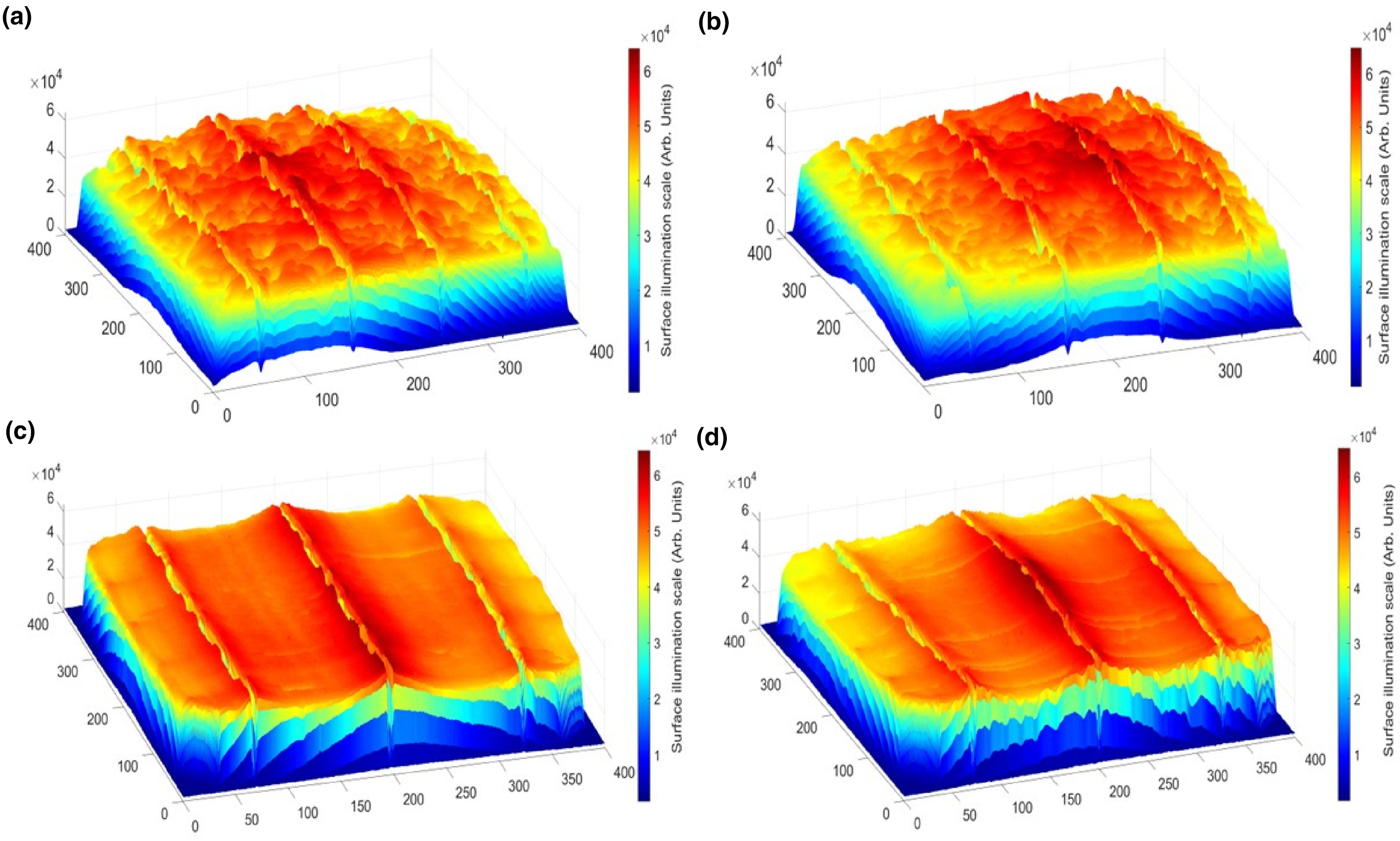
3D illumination diagram of EL images for PS1 (a), PS2 (b), MS1 (c), and MS2 (d), highlighting areas of lower current flow via color scale.
Similarly, Figures 10(c) and (d) the 3D diagrams of cells MS31 and MS2, again demonstrating analogous behavior. The MS1 cell displays high and uniform surface illumination, except at the right end of the cell which has lower surface illumination according to the color scale used. Conversely, the MS2 cell also exhibits high surface illumination, except for the edges of the cell, where there are areas of lower light emission. Analysis of these 3D diagrams suggests that certain structural factors are restricting the surface illumination of the cells during the EL tests.
2D discrete wavelet analysis
The analysis of EL images in the spatial domain was extended to the frequency domain by using the 2D-DWT. This transformation allows for the segmentation of color change speeds within different image pixels based on the desired filtering level. Notably, we utilized a Biorthogonal (Bior) wavelet filter of order 4.4 to decompose the images into two levels.
Figure 11(a) reveals the second-level vertical detail coefficients obtained from the discrete wavelet transform of the PS1 cell's EL image. Notably, several dark red areas are visible over four of the busbars. These markings correspond to the energy density emitted by the current flow through the busbar at the time of EL image capture and directly relate to cell illumination. In Figure 11(b), we observe that the first busbar from left to right exhibits few, if any, red-colored areas (see yellow marks). The associated vertical detail wavelet coefficients appear white, indicating a lower energy density compared to other busbars. This explains the lower surface illumination observed around this busbar in Figure 11(b). Further analysis revealed defective soldering between the cell and the conductor, which can elevate series resistance of the cell and restrict the current flow through that specific busbar.

Second-level vertical detail coefficients from 2D-DWT of EL images for PS1 (a), PS2 (b), MS1 (c), and MS2 (d), highlighting soldering defects on busbars.
Figures 11 (c, d) show the 2D discrete wavelet transforms (DWT) of the EL images for two monocrystalline cells with three busbars, Figure 11(c) shows a significant reduction of the energy density in the last busbar on the right side of the MS1 cell, which is reflected in a lower surface illumination around that area, see Figure 10(c). Figure 11(d) shows a similar phenomenon but in the first busbar of the MS2 cell, which affects the surface illumination in that zone of the cell. Closer physical inspection revealed the presence of welding defects between the cell and the bus bar, which contributed to the phenomenon observed in the 2D wavelet analysis performed.
2D-CWT
To extend the analysis into the frequency domain, the 2D-CWT was applied to the EL images of PS1, PS2, MS1 and MS2 cells evaluated at various current levels. The Cauchy anisotropic mother wavelet was chosen for its sensitivity to wave orientation and image features. Furthermore, its extended support compared to isotropic (non-directional) wavelets allows for capturing finer details during the transformation process. As it is a complex wavelet, only the wavelet modulus is visualized graphically.
Figure 12(a) depicts the graphical representation of the wavelet modulus of the PS1 cell's EL image, with an orientation angle of π radians (180°) and a two-level decomposition scale. At this orientation, the mother wavelet facilitates the observation of the squared magnitude wavelet coefficients on scale 2, which correspond to the energy generated by current flow through the cell's busbars during the EL test. The 3D plot, with its color scale, reveals that lower current flows through the rightmost busbar compared to the others, resulting in reduced illumination around that area (see Figure 10(a)).
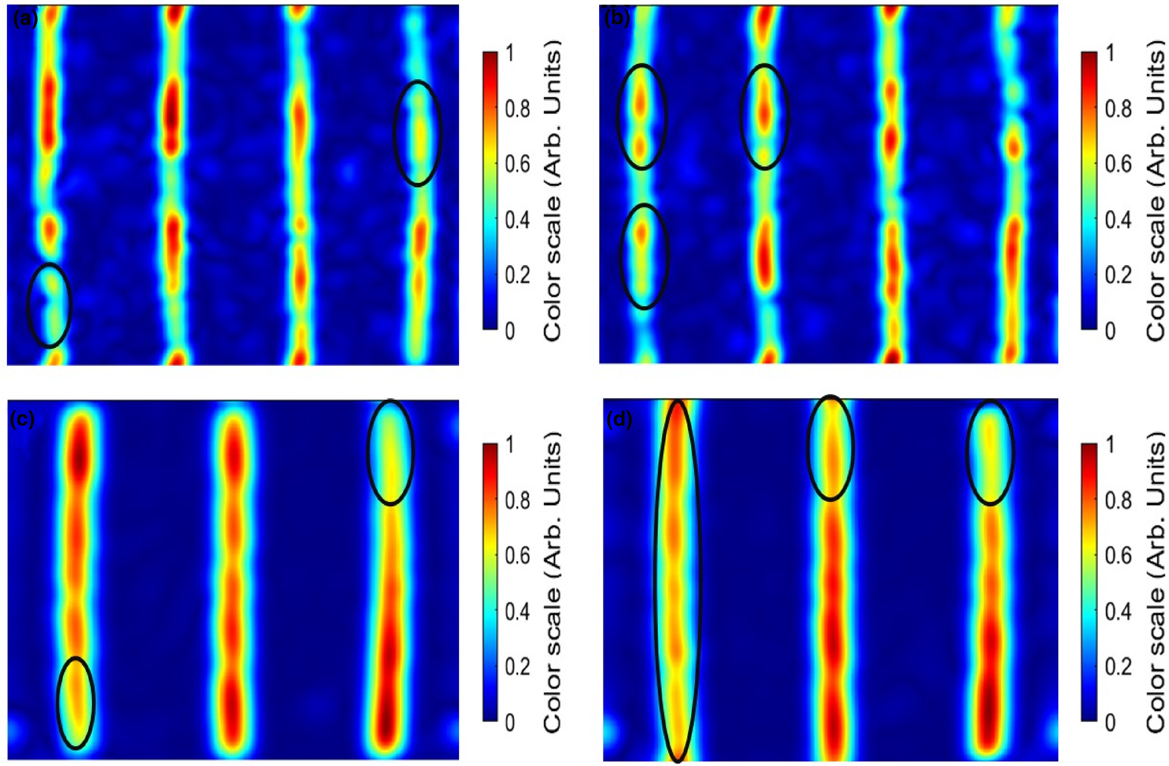
2D-CWT coefficients of EL images: (a) PS1 cell; (b) PS2 cell; (c) MS1 cell; and (d) MS2 cell, indicating variations in spectral energy density.
This observation resembles the previously detected behavior in the 2D Discrete Wavelet Transform representation. The phenomenon can be attributed to a potential electrical contact failure between the electrode and the cell during the welding process, leading to an increased series resistance over time and ultimately restricting current flow across that region of the cell. Figure 12(b) presents the 2D-CWT spatial frequency representation of the PS2 cell's EL image, analyzed with the same parameters (π radians angle and scale 2). This figure reveals a similar situation for the first busbar on the far left of the cell. The 2D wavelet coefficients exhibit a lighter yellow color (see black markings), indicating a lower current flow through the busbar compared to others according to the color scale. This translates to reduced illumination in that specific region of the cell, as observed in Figure 10(b).
Figures 12(c) and (d) show the 2D-DWT of monocrystalline cells with four busbar MS1 and MS2, respectively. The spectral energy density of the MS1 and MS2 cells exhibit variations on certain busbars (areas marked with black ovals). These variations manifest as reduced surface illumination and lower peak power output, replicating the issues observed in the discrete wavelet analysis and other analyzed cells.
This study underscores the diagnostic capability of two-dimensional wavelet analysis for detecting structural and electrical faults in photovoltaic (PV) cells, specifically at the electrode-cell interface. By applying both discrete and CWT on electroluminescence (EL) images of polycrystalline and monocrystalline silicon PV cells, we identified patterns associated with defects that significantly impact cell performance, which are challenging to detect through EL imaging alone.
The grayscale histograms and three-dimensional (3D) color diagrams of the EL images revealed discrepancies in surface illumination, with certain cells exhibiting lower normalized maximum power outputs than comparable cells under identical test conditions. For example, cells with compromised soldering interfaces showed up to a 16.3% reduction in maximum normalized power (MNP), a direct consequence of restricted current flow through specific busbars. This finding demonstrates a quantifiable relationship between current density irregularities and structural flaws that cannot be inferred from EL images alone, confirming the added diagnostic value of wavelet-based analysis.
The implementation of two-dimensional wavelet decomposition proved instrumental in segmenting spectral power density at multiple spatial resolutions, isolating critical frequency bands associated with defective regions. The vertical detail coefficients extracted at the second level provided localized insights into defects at the busbar interface, with affected cells showing up to a 15% decrease in efficiency. These spectral insights support the hypothesis that connection quality between the electrode and cell is a key determinant of PV cell efficiency, and they highlight the importance of robust soldering practices in minimizing power loss due to increased series resistance.
Furthermore, this wavelet-based methodology establishes a foundation for future diagnostic systems incorporating artificial intelligence (AI). By developing classification algorithms capable of estimating series resistance and defect parameters directly from EL images, the proposed approach could enhance defect detection accuracy while reducing reliance on extensive physical testing. The preliminary success in identifying soldering quality as a major factor influencing series resistance suggests that integrating AI with wavelet transforms could yield a powerful tool for automated, non-invasive PV cell assessment.
Footnotes
Acknowledgments
To CONAHCyT and MINCIENCIAS for the doctoral scholarship granted.
Declaration of conflicting interests
The author(s) declared no potential conflicts of interest with respect to the research, authorship, and/or publication of this article.
Funding
The Universidad de Valladolid supported this study with the predoctoral contracts of 2020, co-funded by Santander Bank. This work has been financed also by the Spanish Ministry of Science and Innovation, under project PID2020-113533RB-C33. The Universidad de Valladolid also supported this study with ERASMUS + KA-107.
Statements and declarations section
New affiliation Universidad Nacional Abierta y a Distancia, Bogotá, 111511, Colombia.