
Abstract
Background:
The objective of this work is to develop a highly miniaturized, low-power, biosensing platform for continuous glucose monitoring (CGM). This platform is based on an application-specific integrated circuit (ASIC) chip that interfaces with an amperometric glucose-sensing element. To reduce both size and power requirements, this custom ASIC chip was implemented using 65-nm complementary metal oxide semiconductor (CMOS) technology node. Interfacing this chip to a frequency-counting microprocessor with storage capabilities, a miniaturized transcutaneous CGM system can be constructed for small laboratory animals, with long battery life.
Method:
A 0.45 mm × 1.12 mm custom ASIC chip was first designed and implemented using the Taiwan Semiconductor Manufacturing Company (TSMC) 65-nm CMOS technology node. This ASIC chip was then interfaced with a multi-layer amperometric glucose-sensing element and a frequency-counting microprocessor with storage capabilities. Variation in glucose levels generates a linear increase in frequency response of this ASIC chip. In vivo experiments were conducted in healthy Sprague Dawley rats.
Results:
This highly miniaturized, 65-nm custom ASIC chip has an overall power consumption of circa 36 µW. In vitro testing shows that this ASIC chip produces a linear (R2 = 99.5) frequency response to varying glucose levels (from 2 to 25 mM), with a sensitivity of 1278 Hz/mM. In vivo testing in unrestrained healthy rats demonstrated long-term CGM (six days/per charge) with rapid glucose response to glycemic variations induced by isoflurane anesthesia and tail vein injection.
Conclusions:
The miniature footprint of the biosensor platform, together with its low-power consumption, renders this CMOS ASIC chip a versatile platform for a variety of highly miniaturized devices, intended to improve the quality of life of patients with type 1 and type 2 diabetes.
Keywords
Introduction
Continuous monitoring of metabolites with real-time data analytics is essential for the management of chronic metabolic disorders. 1 Continuous glucose monitoring (CGM) is highly effective in the management of diabetes mellitus 2 and improving the time-in-range (TIR) for both type 1 and type 2 patients. 3
Recent advances in device miniaturization have positively impacted both percutaneous and fully implantable CGMs, in terms of reducing power and implantation trauma, which governs battery life and foreign body response,4,5 respectively. The need for fully implantable CGMs to also embed powering source, processing logic and data communication, in addition to the glucose-sensing element, puts extra burden in comparison with percutaneous CGMs. Light (in terms of both photovoltaics6,7 and fluorescence 8 ) and radio frequency (RF)9 -12 are few of the various methods proposed to eliminate bulky batteries and address data communication with fully implantable CGMs.
As the size of the implant depends on the physical size and power requirements of the embedded processor, the need for smaller and highly efficient logic is paramount.13,14 Shrinking down the dimensions of field-effect transistors has yielded considerable improvement in terms of power, speed, and chip size. In this contribution, we showcase the use of 65-nm technology node in application-specific integrated circuit (ASIC) chips for highly miniaturized CGMs. This yielded a 50% reduction in power savings and 33% reduction in chip footprint as opposed to the equivalent ASIC chip at the 350-nm node. 6 Using this chip, a transcutaneous, long-term (six days), CGM system is demonstrated for small, unrestrained laboratory animals.
Results and Discussion
Earlier reports from our group6,7 have shown results from a custom complementary metal oxide semiconductor (CMOS) ASIC chip using 350-nm technology node. The original architecture, based on current-to-frequency sensor read-out, was retained based on its compact design and low-power consumption. Ιn this work, the highly miniaturized signal processing unit (SPU) architecture, previously implemented in the 350-nm node, 6 was transitioned to 65-nm node. Figure 1a shows the block diagram of the 65-nm ASIC chip with an area of 0.43 × 1.12 mm2 (Figure 1b). This makes it ideal for fully implantable CGM platforms, a topic of future contributions.
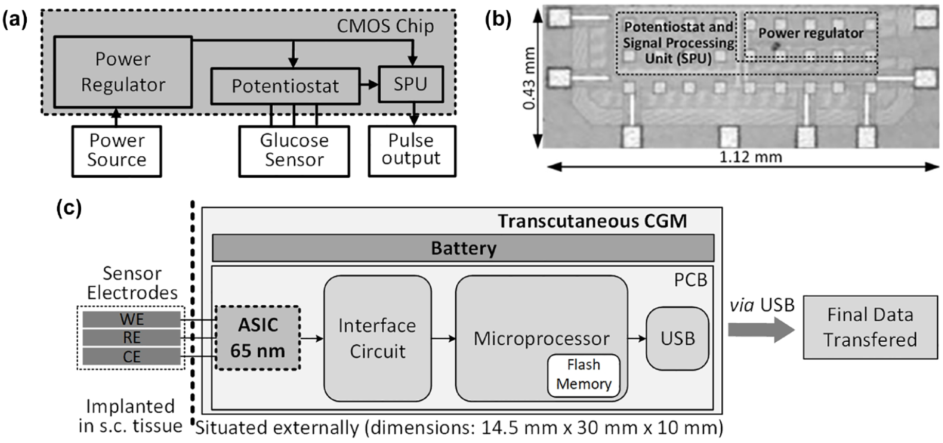
(a) Block diagram of the CMOS ASIC chip, with its top-view image (b). (c) Block diagram of the fully integrated, transcutaneous CGM architecture.
The 65-nm CMOS ASIC chip consists of (1) power regulator, (2) potentiostat that interfaces with the amperometric glucose-sensing element, and (3) an SPU that produces a pulse output. Figure 1c illustrates the block diagram of a transcutaneous CGM system that interfaces the 65-nm ASIC chip with a battery-powered microprocessor, equipped with flash memory storage to save the ASIC’s pulse output frequency values. A universal serial bus (USB) is also provided to retrieve the time-stamped, pulse output frequency values. This results in a 30 × 14.5 × 10 mm3 (length-width-height) transcutaneous CGM platform, suitable for in vivo studies in small laboratory animals.
The amperometric glucose sensor, described in greater detail in Supplemental Information (SI), is composed of three wire electrodes (working electrode, reference electrode, and counter electrode), which are implanted subcutaneously.15-19 The interface circuit in Figure 1c converts the 1.4-V output voltage of the ASIC chip to the 2.5-V input of the microprocessor. The microprocessor performs pulse counting algorithm to measure the frequency of the pulse at predefined intervals of time. The measured frequency during the experiment period is saved onto the flash memory of the microprocessor. At the end of the experiment, the data are saved in the flash memory of the microprocessor and they are transferred to a computer (via USB) for further data display and analysis.
The potentiostat of the 65-nm ASIC chip is composed of an operational amplifier (op-amp) that interfaces with the external sensor electrodes and can read currents in the range of 0.01 to 20 µA. Figure 2a illustrates the circuit block diagram of the 65-nm ASIC chip SPU. The output current of the potentiostat circuit (Isensor) is fed to the SPU via a current-mirror configuration. The mirrored current is used to charge or discharge the capacitor (C0) at different phases. This charging and discharge phenomenon creates a triangular wave signal on the capacitor C0, which is shown in Figure 2a. The triangular wave signal is then converted into a square wave signal using a single-bit analog-to-digital converter (Figure 2a). The time-period of the square wave signal, which is related to frequency, is proportional to the amperometric current of the electrochemical sensor. 20 Figure 2b shows the oscilloscope-captured SPU’s square wave signal, with an output frequency of 11.668 kHz when the input current (Isensor) is 0.6 µA.
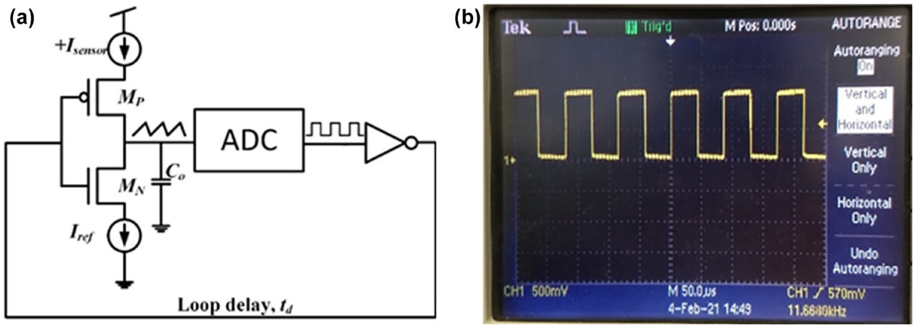
(a) Simplified SPU block diagram of the ADC used to convert the amperometric glucose current values into frequency pulses. (b) Measured SPU waveform of the 65-nm ASIC chip with a frequency output of 11.668 kHz from a current input of 0.6 µA.
Figure 3a and b illustrates the SPU current-to-frequency response on applying an ideal current source in the lower (10 nA to 1 µA) and higher (1 µA to 20 µA) current range, respectively. The measurement results show an excellent SPU linearity with R2 value exceeding 99.8% over the three orders of magnitude current range. This SPU linearity is retained when the 65-nm ASIC chip is interfaced with the microprocessor (Figure 1c).
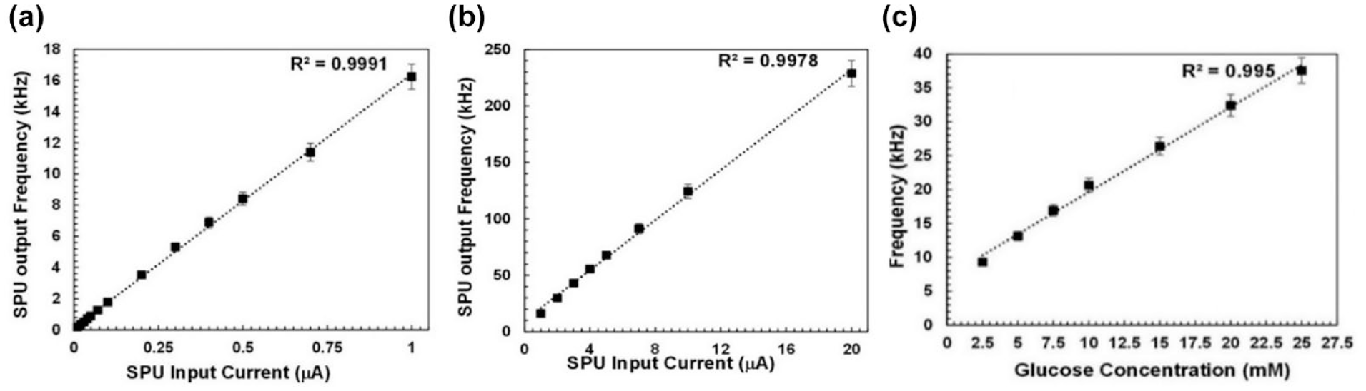
Current versus pulse linear frequency output of the 65-nm CMOS ASIC chip when tested with an ideal input current source from a low (10 nA to 1 µA) (a) to high (1 µA to 20 µA) (b) current range. (c) In vitro frequency response of the 65-nm ASIC chip when integrated with an amperometric glucose-sensing element (Figure 1c) over the entire glycemic (45-50 mg/dL) range.
Figure 3c illustrates the frequency response versus glucose concentration. In a similar fashion to ideal current source, the amperometric glucose-sensing element (discussed in SI) provided a linear frequency response (R2 = 99.5%), with a sensitivity of 1.21 × 10+3 Hz/mM over the entire glycemic range. Such sensitivity varies by circa 10%, based on sensor-to-sensor variability. The average current consumption of a sensor-interfaced 65-nm ASIC chip is 20 µA, whereas for the fully integrated CGM architecture of Figure 1c, which includes the microprocessor, it is 600 µA.
In Vivo CGM Testing
Rat metabolism, physiology, and pathology are considered much closer to humans, as opposed to those of mice. 21 Accordingly, the compact, low-power consumption device incorporating the 65-nm ASIC chip, if appropriately configured, can provide long-term, continuous glucose and other metabolite monitoring results for unrestraint rats exposed to a variety of well-controlled stimuli (ie, diet, stressors, pathology, genetic predisposition, etc).
Typically, the maximum weight that can be imposed to a laboratory animal is circa one-tenth of its weight. 22 With an average weight of a young rat at circa 150 g, the maximum weight of an external device should not exceed 15 g. The transcutaneous device of Figure 1c weighs only 6.1 g (including 100-mAh LiPo battery), which is circa 40% of the maximum allowed load to be imposed on a young rat.
Figure 4a illustrates the long-term, in vivo, frequency response of the transcutaneous device of Figure 1c attached on an unrestrained, healthy, male, Sprague Dawley rat. The microprocessor was programmed to obtain a glucose value once every 3 minutes. Sensor warm-up data of day 1 are not shown. With a 3-minute data collection interval, the battery lasted for circa six days. Following battery recharge, the transcutaneous sensor operated for another six days. The collected 65-nm ASIC chip frequency values were plotted as is, and no data smoothing has been performed. Barring few spikes, which can be readily excluded with further data processing, the transcutaneous sensing device demonstrates good stability.
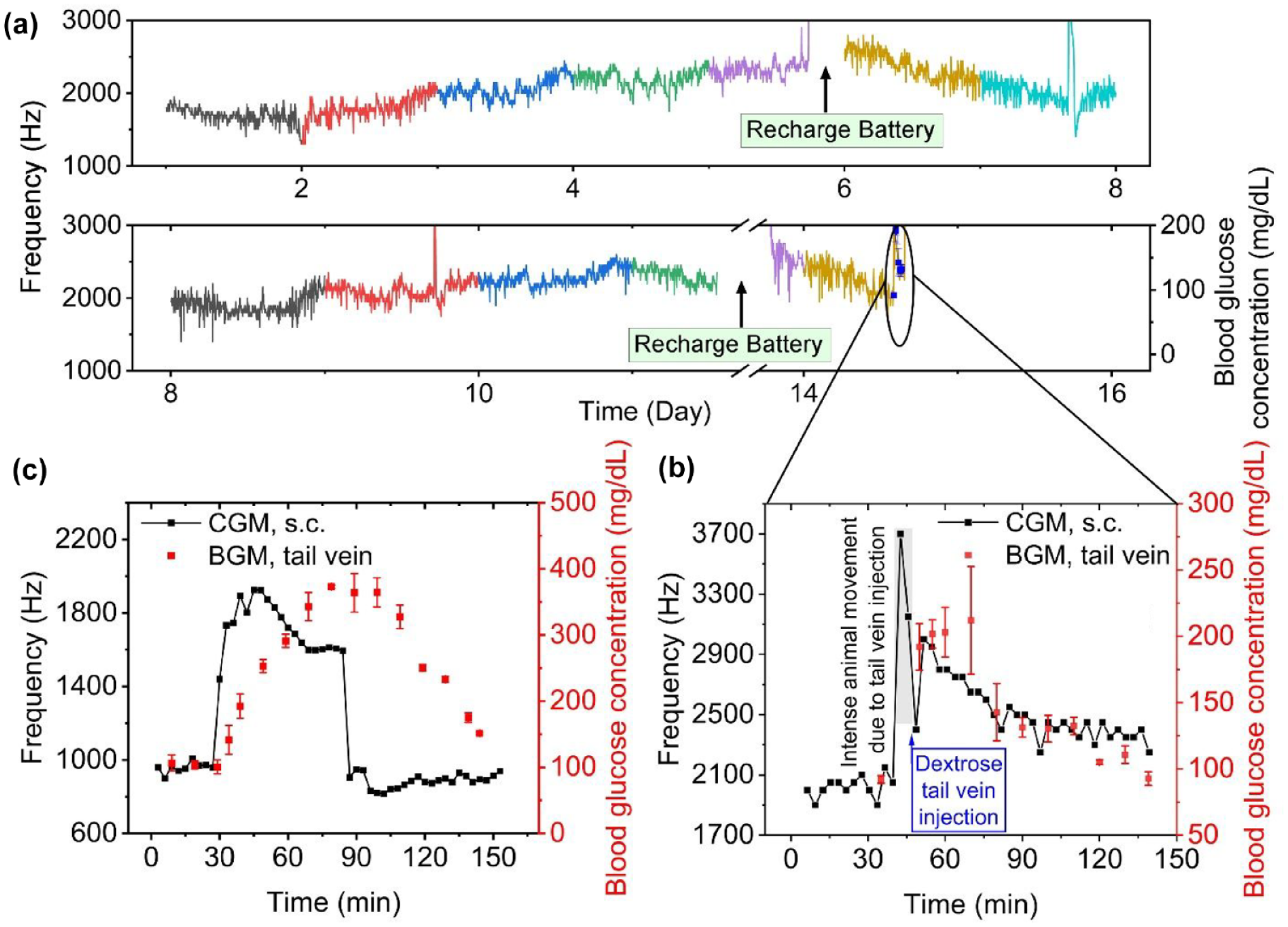
(a) Continuous in vivo monitoring of the subcutaneous glucose levels from an unrestrained, healthy rat using the transcutaneous sensing device of Figure 1c. Collected frequency values (every 3 minutes) were interpolated and plotted without data smoothing. Single battery charge lasts circa six days. Sensor warm-up (day 1) is not shown. On day 14, a glycemic uprising event was induced and is shown in (b), together with tail vein blood glucose values (collected in triplicate). (c) In vivo frequency response and blood glucose value variation upon isoflurane-induced anesthesia of a healthy, nonfasted, rat.
Figure 4b illustrates a close-up of a glycemic uprising event induced by intravenous tail vein dextrose injection to a nonanesthetized, healthy, male, Sprague Dawley rat, after 14 days of sensor implantation. While transferring the nonfasted rat from its cage into the restrainer tube (by suspending it from its tail), the rat was highly agitated. The high sensor reading prior to tail vein dextrose injection (shown in the gray) can originate from:
Changes to the microenvironment around the implanted electrodes, and
Release of excessive counter-regulatory hormones (ie, glucagon, growth hormone, glucocorticoid, etc) and neurotransmitters (ie, endorphins, catecholamine, norepinephrine, etc), leading to increased glucose production. 23 A recent microdialysis study relates rising subcutaneous glucose values of rats when exposed to stress (tail suspension), 24 albeit the increase is not so pronounced for healthy rats.
Upon tail vein dextrose injection (50 minutes plus), both the subcutaneous recorded frequency and blood glucose values show a pronounced increase with respect to the 35-minute “rest values” (Figure 4b). Within the next 30 minutes, both the elevated sensor frequency and blood glucose levels subside as expected for a healthy rat.
To further evaluate the in vivo glucose-sensing performance of the 65-nm ASIC chip, the effects of anesthesia on the glucose levels of healthy, nonfasted rats were investigated. A variety of studies have shown that certain anesthetics could induce a well-pronounced hyperglycemic response on nonfasted laboratory animals.25-28 Ward et al 28 have observed a profound hyperglycemic response in rabbits by general inhalation anesthesia via both the subcutaneous amperometric glucose sensor and blood glucose sampling.
Figure 4c illustrates the in vivo frequency response together with tail vein blood glucose values of a healthy, nonfasted, male, Sprague Dawley rat. Here, a two-point calibration was used to correlate the baseline and peak-level frequencies to those of blood glucose levels. The transcutaneous implant shows a rapid (within three minutes) increase in sensor frequency following anesthesia administration. This increase reaches a maximum within 20 minutes followed by a gradual drop and equilibration at high-frequency values. A similar trend has been observed by Ward et al, 28 which matches exactly the rapid increase, gradual drop, and equilibration at high glucose values, during anesthesia. In this study, following the anesthesia administration,29-31 the subcutaneous frequency increase is much steeper than that observed in Ward’s report. 28 This might be due to faster electrochemical sensor response (ie, 40 seconds for the sensor of Figure 2a) or difference in the anesthetic agent (ie, isoflurane vs halothane in Ward’s report). 28 These results confirm the efficacy of the subcutaneously implanted sensor in detecting in vivo glycemic events and show the great potential of using this sensitive and fast responding glucose detection platform in future diabetes and metabolic studies for humans, as well as for small, unrestrained, laboratory animals.
Supplemental Material
sj-docx-1-dst-10.1177_19322968231153419 – Supplemental material for Highly Miniaturized, Low-Power CMOS ASIC Chip for Long-Term Continuous Glucose Monitoring
Supplemental material, sj-docx-1-dst-10.1177_19322968231153419 for Highly Miniaturized, Low-Power CMOS ASIC Chip for Long-Term Continuous Glucose Monitoring by Raja Hari Gudlavalleti, Xiangyi Xi, Allen Legassey, Pik-Yiu Chan, Jin Li, Diane Burgess, Charles Giardina, Fotios Papadimitrakopoulos and Faquir Jain in Journal of Diabetes Science and Technology
Footnotes
Acknowledgements
The authors also acknowledge the skillful assistance of Mr. Jiuzhou Zhao and Dr. Jun Kondo in various aspects of the project.
Abbreviations
ADC, analog-to-digital convertor; ASIC, application-specific integrated circuit; CGM, continuous glucose monitoring; CMOS, complementary metal oxide semiconductor; SPU, signal processing unit.
Declaration of Conflicting Interests
The author(s) declared the following potential conflicts of interest with respect to the research, authorship, and/or publication of this article: Faquir Jain and Fotios Papadimitrakopoulos declare financial conflict of interest as Biorasis co-founders.
Funding
The author(s) disclosed receipt of the following financial support for the research, authorship, and/or publication of this article: The authors thank the US Army grant #W81XWH-15-C-0069, JDRF grant #2-SRA-2017-505-S-B, and Helmsley Charitable Trust for financial support.
Supplemental Material
Supplemental material for this article is available online.
References
Supplementary Material
Please find the following supplemental material available below.
For Open Access articles published under a Creative Commons License, all supplemental material carries the same license as the article it is associated with.
For non-Open Access articles published, all supplemental material carries a non-exclusive license, and permission requests for re-use of supplemental material or any part of supplemental material shall be sent directly to the copyright owner as specified in the copyright notice associated with the article.