
Abstract
The electronic and structural properties of silicene, multilayer silicene, and 2D silicon films, synthesised on Ag(111), Au(111) and on the α- and β-phase Si(111)√3 × √3R30°-Bi, have been reviewed according to the results of investigations made by low energy electron diffraction, Auger electron spectroscopy, grazing-incidence X-ray diffraction, low/high electron energy diffraction, reflection electron energy loss, scanning tunnelling microscopy as well as spectroscopy, and density functional theory calculations. The findings revealed the successful growth of silicene and multilayer silicene on Ag(111) single crystal, and on the α-phase Si(111)√3 × √3R30°-Bi, while, at variance, two-dimensional Si islands (2D Si) still showing the √3 × √3R30° reconstruction, parallel to that of bismuth, were obtained on the β-phase Si(111)√3 × √3R30°-Bi. Single layer of blue phosphorus synthesised on Au(111) single crystal and on Te/Au(111), were also reviewed, and compared to silicene deposited on Ag(111) single crystal, as well as to their first-principles density functional theory calculations to show their interesting structural properties.
Keywords
Introduction
Silicene and other 2D elemental materials
Silicene, one atom thick of silicon arranged in a honeycomb lattice, was synthesised for the first time in 2012, after assigning, in 2010, of the Nobel Prize in Physics: “for groundbreaking experiments regarding the two-dimensional material graphene”, 1 one atom thick of carbon arranged in a honeycomb lattice. 2 Later, and with the awareness that syntetic materials, under suitable experimental conditions, can be synthesized in laboratory, in ultra-high vacuum (UHV), although on their own they were not, by their nature, inclined to spontaneously adopt their new found allotropic forms. This was, for instance, the case of silicene, and/or its multilayer silicene,3–16 and other 2D elemental materials of group IVA, such as germanene,17,18 plumbene,19,20 and stanene, 21 and of group VA, as single layer of blue phosphorus, 22 arsenene,23,24 antimonene, and bismuthene25,26 that were successful synthesized, as exausthively reported in a recent review. 27
Indeed, going beyond, not only the elements of groups IVA and VA of the periodic table, can adopt a honeycomb-like arrangement, but also, for example, group IIIA, with borophene, 28 and gallenene,29,30 group IVB, with hafnene, 31 and VIA, with selenene 32 and tellurene. 33
In the case of silicene, alternative substrates to the single crystal Ag(111), where it was initially discovered, 3 such as, for example, Au/Si(111), 4 diboride thin films, 34 Ir(111), 35 and after the formation of the Ag-Si(111) interface, or Bi-Si(111), used, recently, as templates, have been intensively investigated.8–16 This was also done for the synthesis of layers above the first, leading to a new allotropic form of silicon, namely: multilayer silicene, composed by alternating stacks of honeycomb-like layers.8–16
Although the feasibility of this silicene layered structure, the multilayer silicene, has been debated, 36 experimental measurements and first-principles theoretical calculations have given their inequivocal synthesis evidence.8–16,37,38 In addition, from technological point of view, a strong resistance towards air degradation was proved for multilayer silicene,8,39 and the field-effect transistor (FET) devices for both silicene and multilayer silicene, have been already realized, as well as the exploiting of silicene and Xene materials in biosensing, optoelectronics and biomedicine applications.40–49
In particular, in this mini review, we want to underline the structural similarity between the single layer silicene/Ag(111), 3 and the single layer blue phosphorus/Au(111), 22 as well as Te/Au(111). 50 This aims to highlight how, far from trivial, in all these cases the honeycomb-like structure, although not favored by nature, appears with similar reconstructions, with different elements and on different substrates.
The layered phase of phosphorus: “Blue phosphorus”
Polymorphic phosphorus, P, belonging to the VA nitrogen group of the pnictogen elements, shows three main allotropic phases in its solid form, named white, red, and black phosphorus (BP). The white P, is a tetraphosphorus (P4) molecular solid, with a translucent waxy appearance. The red P is an amorphous polymeric solid powder. The BP, obtained already in 1914, by applying a high pressure of about 1.2 GPa to white P at a temperature of 200°C, 51 is similar in appearance to graphite, with a puckered structure of linked sheets of atoms. The structure of black phosphorus consists of double layers; the unit cell is side-centered orthorhombic with a = 3.31 Å, b = 4.38 Å and c = 10.50 Å.51,52
Ab initio calculations were computed to investigate a new layered phase of phosphorus, called blue phosphorus. 53 This phase was found stable as the black phosphorus, which is considered the most stable phosphorus allotrope at RT,54–56 with its nonplanar honeycomb-like lattice, exhibiting a wide fundamental indirect band gap in excess of 2 eV. 53
Indeed, the 2D counterpart of layered black phosphorus, named phosphorene, was found a p-type semiconducting material, with a direct, and appreciable band gap, of 1 eV, wider than the bulk value of 0.31–0.36 eV.54–56 In addition, ab initio calculations 56 indicated that this direct band gap, depends on the number of layers and their in-layer strain, scaling as the inverse of the number of layers N in a few layer slab, 56 and promising novel optoelectronic devices. 27 Thus, a photoluminescence peak of single-layer phosphorene was observed in the visible optical range, confirming that the band gap is larger than that of the bulk structure. Furthermore, the transport measurements indicated a high hole mobility, permitting the realization of p-type field-effect FET, by few-layers phosphorene.56,57
On different methods to prepare buckled/flat silicene, blue phosphorus, and their electronic properties
Among the techniques for obtaining single layer silicene, in addition to the UHV-MBE growth from solid source, it is worth mentioning that the atomic diffusion technique of Si through a heterostructure such as zirconium diboride (ZrB2) (0001), 34 and Au(111),4,5 deposited in the form of a thin film on Si(111), from the underlying Si(111) substrate.4,5,34
The Si substrate serves as a lake of silicon atoms for the synthesis of a surface layer overlying the entire heterostructure. In fact, by applying a suitable temperature to these systems, the silicon atoms can migrate towards the surface and reconstruct it in the form of a single silicon layer organized as an artificial honeycomb structure. In particular, the basic scientific interest in the Au/Si(111) system lies in the experimental demonstration of the synthesis of a flat silicene, on the contrary to the initial density functional theory (DFT) calculations, which only predicted the existence of a free-standing buckled silicene. 58
This fact, in addition to unveil innovative physical properties, compared to the buckled form initially obtained on Ag(111), and predicted by theoretical calculations 58 for free-standing silicene, introduces the important fundamental possibility of obtaining honeycomb silicon, which had been denied until then, promising its potential synthesis on other different substrates. Hence, from this derives the unexpected and surprising adaptability of silicon atoms to assume hybridizations different from the usual sp3, believed to be unique until now, worthy of being reported together with buckled silicene on Ag(111).
Besides, the importance of the existence of new allotropic forms of silicon, silicene and multilayer silicene, which makes these 2D materials interesting, lies in their peculiar electronic properties that place them in the group of the so-called Dirac materials. 59 In Dirac materials the electrons can behave as massless particles,3,11,12 whit a gap of about 0.2 eV at the Γ point of the Dirac cone. In the case of epitaxial planar silicene, grown on the Au(111) film deposited on the Si(111) substrate, the electronic properties evidenced Dirac-dispersed 1D bands. 5
Monolayer and multilayer phosphorene were prepared by several methods, these include liquid and electrochemical exfoliation, mechanical exfoliation,55–57,60,61 pulsed laser deposition and plasma assisted thechniques,62,63 and chemical vapor deposition. 64
Single layer blue phosphorus, in addition, was synthesized using ultra high vacuum (UHV) molecular beam epitaxial (MBE) growth on single crystal Au(111) producing the (4 × 4)/(5 × 5) reconstruction. The black phosphorus served as precursor. The system was predicted by means of DFT calculations, and investigated by low temperature scanning tunneling microscopy (STM), and scanning tunneling spectroscopy (STS), finding a gap of 1.10 eV. 22
Silicene and blue phosphorus on several templates: Advanced features
This work reviews for the first time, the results of the experimental genesis of silicene, 3 compared with single layer of blue phosphorus grown on Au(111), 22 and Te/Au(111), 50 which shows a striking similarity in the atomic arrangement, and the multilayer silicene, recently obtained on the α-phase and β-phase Si(111)√3 × √3R30°-Bi,9,65,66 as well as in the past, on different substrates.8,10–16 A set of complementary techniques, used to investigate such structures, such as Auger electron spectroscopy (AES), X-ray diffraction (XRD), grazing-incidence X-ray diffraction (GIXRD), low/high electron energy diffraction (LEED/RHEED), reflection electron energy loss spectroscopy (REELS), scanning tunnelling microscopy/spectroscopy, along with ab-initio density functional theory calculations, are reported. The first synthesis of flat silicene on Au(111)/Si(111) surface,4,5 by means of thermal surface segregation process is also rewieved, to underline how silicon atoms are capable of adopting allotropic structures that are not exactly favourable to it, but, artificially physical possible.
In the context of surface physics of condensed matter, and/or 2D materials, the synthesis of new solid allotropes of silicon, silicene and multilayer silicene, is, usually, denied. It can often be argued that the synthesized structures do not exhibit the electronic characteristics of the free-standing silicene. However, the discovery of the sp 2 -like chemical hybridization of silicon valence orbitals in silicene and multilayer silicene, now represents a real breakthough in solid state physics, which has paved the way for the discovery of numerous so-called, –elemental-ene materials.
In particular, the opportunity to use the Bi atoms as a matrix for silicene and multilayer silicene films, in heteroepitaxial growth, reveals the prospect of new fascinating properties in the framework of topological insulators, with high spin-orbit coupling. 67
In the case of silicene and single layer of blue phosphorus, the similarity of surface structure is clearly underlined, even though they are allotropes of different chemical elements, Si and P, synthesised on different substrates, Ag(111), Au(111), Te/Au(111), and Si(111). Furthermore, silicene was synthesised on Au(111)/Si(111) by a thermal surface segregation process, completely different from the solid Si deposition, producing the flat silicene, as opposed to the buckled silicene obtained on Ag(111).
All of these meaningiful experimental findings, were in very good agreement with first-principles density functional theory calculations, recently reported.3–5,22,50
Content and purposes
The fundamental intention of this work is to give the deserved recognition to silicene-multilayer silicene and single layer of blue phosphorus above all to physics, which manifests itself through symmetries and analogies of properties, as soon as experimental conditions make it possible, as demonstrated by the significant examples illustrated here.
One of the aims of this work was to compare the growth of silicon atoms on the two Bi interfaces, α- and β-phases of Bi on Si(111) substrate, having the same reconstruction, but with a different number of Bi atoms in the surface unit cell. This gives to Si adatoms the possibility of forming either a silicene layer, which then evolves into multilayer silicene, or a two-dimensional (111) silicon layer, which subsequently transforms into Si(111) 2D islands. Considering that the Bi-Si(111) interface is extremely relevant as it is the seed of important fundamental physical properties, such as topological insulator characteristics, or the capability to host quasiparticles as Majorana fermions, thus, one could extrapolate that both silicene and single silicon layer, deposited on α-, and β-Bi phase, could represent a new field of intense future investigations. Very interestingly, buckled single layer of blue phosphorus and flat silicene were epitaxially grown on Au(111), and Te/Au(111), respectively.
Another pourpose of this paper is to enphatize that the existence of silicene, buckled and flat, and its multilayer is confirmed, which gave rise to the search and then discovery of new unexpected allotropic phases of elements of the periodic table, and/or their heterostructures under specific experimental conditions.
Methods of the reported heterostructures
The experimental conditions used to synthesize silicene, multilayer silicene, and phosphorene were exhaustively reported in Refs. 3, 4, 9, 22 and 66. The synthesis of these materials takes place in UHV (1.2 • 10 −10 mbar) by epitaxial growth on clean, silver (111) (1 × 1), gold (111) (1 × 1) and Au(111) (1 × 1)/silicon (111) (7 × 7), as well as on α- and β-phase Bi/Si (111) substrates. Single crystal substrates were typically prepared by several cycles of Ar+ ions bombardment (1.5 kV, 5 • 10 −5 mbar), and annealed at about 540°C for several minutes, in order to obtain the (1 × 1) surface; while the (7 × 7) reconstruction of Si(111) surface was obtained after several annealing at ∼ 1150°C in a low vacuum environment of about 5 • 10 −10 mbar. LEED, RHEED, and AES were applied to study the surface reconstructions and the electronic properties of the deposited 2D materials. AES spectra (EP = 2.5 keV, CMA- PHY 255G double-pass) were recorded in first derivative mode, with, at least, 0.5 eV resolution. A Bragg-Brentano Panalytical Empyrean diffractometer (ceramic anode Cu, 40 kV, 40 mA), was used both in plane and out-plane, to perform XRD, and GIXRD measurements; while STM (Omicron LT-STM/VT-STM) experiments, probing in constant current topography and in STS modes, were carried out at room temperature (RT). Knudsen evaporation cells were employed for the deposition of Bi and P, while a solid Si source, consisting of a heated Si-wafer piece, was used for the deposition of silicene and multilayer silicene, from a thickness of 0.5 up to, at least, 5 monolayers (ML), while the Ag and Si substrates were kept at temperature of ∼200°C.3,9–15 The α-phase Si(111)√3 × √3R30°-Bi, was obtained keeping the Si(111) at ∼350°C, and evaporating Bi up to ∼1/3 ML, 9 instead, for the β-phase Si(111)√3 × √3R30°-Bi, Si was kept at ∼250°C, and Bi thickness set up to ∼1 ML. 66
The synthesis of the flat silicene was performed on a thin film of Au(111) grown on Si(111). The (7 × 7) reconstruction of the clean surface of Si(111), performed in UHV, was passivated by forming the 6 × 6-Au reconstruction, depositing on the surface 1.5 ML Au into clean Si(111) surface, and then adding on this hetero structure at RT, several Au(111) monolayers (about 10 ML). The gradual annealing of the sample up to 290°C, produced the flat silicene, through a surface segregation process. RHEED was used to monitor the sample growth during all stages of the process.4,5 Finally, first-principles density functional theory calculations were also performed for all hetero structures studied.
Single layer blue phosphorus was obtained on Au(111). After cleaning the Au(111) substrate and subsequent annealing at 500°C, phosphorus was deposited by evaporation from a crucible containing bulk black phosphorus at 260°C, keeping the substrate temperature below 260°C. Alternatively, the substrate was also kept at RT and was post-annealed at 250°C for 60 min. 22 Furthermore, phosphorous was deposited on Te(Au(111) kept at 250°C, by evaporating the bulk black phosphorus, at 290°C. The monolayer of tellurium (Te) was evaporated at 200°C on Au(111) kept at 300°C.50,68,69
Results and discussion
This section reports the main results of the growth and characterization of silicene and blue phosphorus. It includes the following paragraphs: – Silicene on Ag(111) single crystal, and single layer of blue phosphorus on Au(111) single crystal, and Te/Au(111) single crystal; – Flat silicene on Au(111)/Si(111) single crystal: – Silicene and multilayer silicene on Bi/Si(111), review the main results of growth and characterization of silicene, multilayer silicene and single layer of blue phosphorus.
Silicene on Ag(111), single layer of blue phosphorus on Au(111) single crystals and on Te/Au(111) single crystal
Figure 1(a) reports the experimental and theoretical structural results, in the real space, on the first synthesis of silicene on a single crystal Ag(111) (1 × 1), attested by the honeycomb-like structure observed on the large filled-states STM image.
3
The atomic structure is detailed in the high-resolution (HR) filled-states STM image of Figure 1(b). This HR-STM image, artistically, evokes neatly arranged flowers with dark centres, whose distance, marked by the yellow line, is 11.4 Å. This is the silicene unit cell side, corresponding to the (4 × 4)/(3 × 3) symmetry, with respect to Ag(111) 1 × 1 and silicene (1 × 1) structures. Thus, regularly wide distances are reported in (c), along the line profile traced on the dashed white line in the STM image of (a), illustrating a regular distance pattern of 11.4 Å between the various crests. To support these experimental findings, first-principles DFT calculations were performed.
3
The top- and the side-view of the fully relaxed silicene atomic geometries on Ag(111) substrate are shown in Figure 1(d) and (e), where, in yellow, is reported the silicene 4 × 4 unit cell. Here, we can observe a honeycomb arrangement of the orange colored Si atoms, placed directly above the silver atoms in gray, and the yellow ones, placed in between the silver atoms. The white circle in Figure 1(d) contains a single hexagonal silicene ring, whose calculated structural characteristics are reported in 1 (e) and 1 (g), showing the details of the structure, where the simulated STM image of the silicene structure 1 (d) is showed in 1 (f). It is clearly evident that we are in presence of a displacement of the two atomic planes, between the orange and yellow Si atoms, which confers to silicene a buckling of 0.75 Å, and a distance of 2.32 Å between two adjacent atoms in the honeycomb ring.
3
Interestingly, the simulated image in Figure 1(f) exhibits the same structural features as those observed in the experimental STM image of 1 (b), evidencing a hexagonal arrangement of a triangular structure around dark centres. (a) Filled-states STM image of silicene grown on single crystal Ag(111) 1 × 1, evidencing the honeycomb-like structure; (b) high resolution filled-states STM image, showing the silicene atomic arrangement, with the distance between the dark centres, (yellow line), of 11.4 Å, which is the silicene unit cell, corresponding to 4 times the Ag(111) lattice constant; (c) line profile traced along the dashed white line reported in (a), (d) top, and (e) side view of DFT structural calculations for fully relaxed silicene atomic geometries on Ag(111); (f) simulated STM image of the structure (d); (g) expanded image of the single hexagonal silicene ring marked in (d) with the white ring. The silicene 4 × 4 unit cell, in yellow, is marked in (e). Reprinted (Figures 2 and 5) with permission from P. Vogt, P. De Padova, C. Quaresima, J. Avila, E. Frantzeskakis, M. C. Asensio, A. Resta, B. Ealet, and G. Le Lay, Phys. Rev. Lett. 108 155501, Copyright (2012) by the American Physical Society.
It should be highlighted that the spatial arrangment of the Si atoms in the yellow unit cell of Figure 1(d) contains eighteen atoms, six of which, the orange ones, occupy the vertices of the two opposite triangles, lying on the upper layer. 3 They are directly located above the silver atoms, represented by the grey spheres in Figure 1(d). 3 The simulated image in Figure 1(g) shows the α bond angle of about 110° for the six orange atoms, very close to the angle of 109.5° of an ideally sp3 hybridized Si atom. For the remaining twelve yellow Si atoms, six are pure sp2 hybridized, with β bond angles of about 120°, and six have bond angles between about 112° and 118°, indicating a mixed sp2/sp3 hybridization. 3
Keeping the Au(111) substrate at 230°C, the precursor of the black phosphorus, was deposited, 22 forming large domain size as showed in the STM image of Figure 2(a), which evidences an ordered honeycomb-like structure, as silicene, and/or graphene.70,71 Figure 2(b) shows the STM image, acquired at high-resolution, where the dark centres are surrounded by six ordered triangles. 22 Figure 2(c) presents the line profile corresponding to the red line traced in 2 (b), with a distance between of each crest of 14.7 Å, which represents the sides (a,b) of the (5 × 5)/(4 × 4) unit cell of phosphorene, in yellow, in Figure 2(b). Top and side view of the DFT optimized model of single layer blue phosphorus on Au(111) are reported in Figure 2(d) and (e), respectively. Here, the phosphorus atoms of the upper layer are reported in purple spheres, while the ones of P and the Ag, belonging to the underlying layers, are in yellow and in grey, respectively. Such arrangment gives to the phosphorene a buckling of (3.58 - 2.40) Å = 1.18 Å, as can be seen from Figure 2(e). The simulated STM image is displayed in Figure 2(f), according to the structural model reported in 2 (d). The top and the side view of the atomic model of single layer of blue phosphorus are reported in Figure 2(g), with the unit cell side of 3.28 Å. 22 The phosphorene 5 × 5 unit cell, with respect to silver substrate, in yellow in Figure 2(d), contains thirty-two P atoms, in such way allocated: twelve in the two opposing triangles, six with the vertex facing up, and six with the vertex facing down; the purple P atoms, as can be easily observed in the HR-STM image of Figure 2(b), and in its simulation 2 (f), the remaining yellow P atoms located in the underlying layer. 22
From panel (d) of Figure 2, it can be observed that the purple P atoms, depicting the triangles occupy positions between the Ag atoms, and are not directly above Ag atoms, as is the case in the silicene, in Figure 1(d). (a) STM image of single layer of blue phosphorus grown on single crystal Au(111) 1 × 1, evidencing the honeycomb-like structure; (b) high resolution STM image, showing the phosphorene atomic arrangement, with the distance between the dark centres of 14.7 Å, which is the phosphorene unit cell, yellow, corresponding to 5 times the Au(111) lattice constant; (c) line profile traced along the red line reported in (b). The DFT structural calculations for fully relaxed phosphorene atomic geometries on Au(111) substrate are reported in (d) top, and (e) side view, top- and bottom-layer of phosphorus atoms are purple and yellow balls, while the Au substrate atoms are the grey balls; (f) simulated STM image of the structure (d); (g) top- and side-view atomic model of blue phosphorus, with b1 = b2 = 3.28 Å. Adapted from Figures 1–3 of Ref. 22, Copyright © 2016 American Chemical Society, CCC Right link.
A similar atomic arrangement for phosphorene was also obtained by depositing P on the Te/Au(111) interface. 50 A monolayer of Te on Au(111) was hexagonally arranged, forming a suitable buffer layer that acted as a template for the synthesis of a single layer of the blue phosphorus. Indeed, phosphorene flakes, of different sizes, were found on the Te layer. These phosphorene flakes formed hexagonal honeycomb structure consisting of dark hole surrounded by six equilateral triangles, 50 exactly as shown in Figure 2(b) above, 22 demonstrating besides the presence of a new template for the growth of single layer blue phosphorus, 50 also its fully similarity to the silicene flower structure. 3
As it can be easily observed, the structural pattern of single layer of blue phosphorus, deposited on Au(111), 22 as well as on Te/Au(111), 50 and silicene, deposited on Ag(111), 3 in addition to unveil a beautiful artistic design, combining art/beauty and physics, like flower petals, are extremely similar, apart from the different number of atoms contained in the two different unit cells, for reasons related to symmetry and epitaxy, as expected.
This fact, far from trivial, actually encompasses all its physical importance. First of all, it should be noted that the elements P and Si belong to different groups, the VA and the IVA of the periodic table, not favoring similar physical properties, in principle neither electronic nor structural.
On the contrary, surprisingly, as demonstrated, they share a similar atomic arrangement, under their appropriate growth conditions, on different substrates.3,22,50 This awakens, exactly, their new allotropic nature, directly related to new Van der Walls type materials, irrespective of their relative positions above the atomic arrangement of the substrates,3,22,50 while still retaining the symmetry, but with a nature σ (σ*), π (π*), proper to a honeycomb lattice.
Flat silicene on Au(111)/Si(111)
A new silicon allotrope, named planar silicene, was epitaxially grown on Au(111) thin films in the process of surface segregation.4,5 Figure 3(a) reports the STM image at atomic resolution, revealing a flat honeycomb silicene, which manifests through deformed hexagons and pentagons (see coloured drawings) possibly induced by the presence of vacancies on the surface. The line profile shown in Figure 2(b), obtained by following the semi-random green path of (a), clearly attests the flatness of silicene, being its roughness (buckling) less than 5 pm, i. e. an order of magnitude lower than in free-standing silicene, and the lattice constant accordingly longer.
First principles density functional theory calculations are illustrated in panels (c), (d) and (e) of Figure 3, and are in good agreement with the experimental results: the perfect flat honeycomb Si lattice has the Au atoms located in hollow sites below the Si layer, with a calculated lattice constant of 4.10 Å; whereas the angles between Si atoms are uniform, yielding 120°, confirming the pure sp2 hybridization of Si.
4
In Figure 3(e) the separation between the Au and silicene layers is marked, and is equal to d = 1.30 Å, while the Si-Au bond is 2.70 Å. This chemical bond was found to have a ionic character, where each Au atom in the unit cell receives a charge of 0.46 e from the neighbour Si atoms. As shown in Figure 3(d), by charge density distribution, the covalent bonds are probed only between Si atoms.
4
(a) High-resolution STM image of planar silicene on Au(111)/Si(111) substrate. (b) Line profile along the zig-zag green line marked in (a); (c) top- and (d) side-view DFT structural model calculations of a flat silicene/Au(111) system. Si atoms are in light blue, and Au atoms in yellow. (e) is the charge density isosurface calculated at the isovalue of 3 × 10⁻³ e Å−3. The black unit cell is marked in black in (c), and in (e) d is the distance between the silicene layer and the top Au atoms. Adapted from Figures 2 and 3 of Ref. 4, Copyright © 2019 WILEY-VCH Verlag GmbH & Co. KGaA, Weinheim, CCC Right link.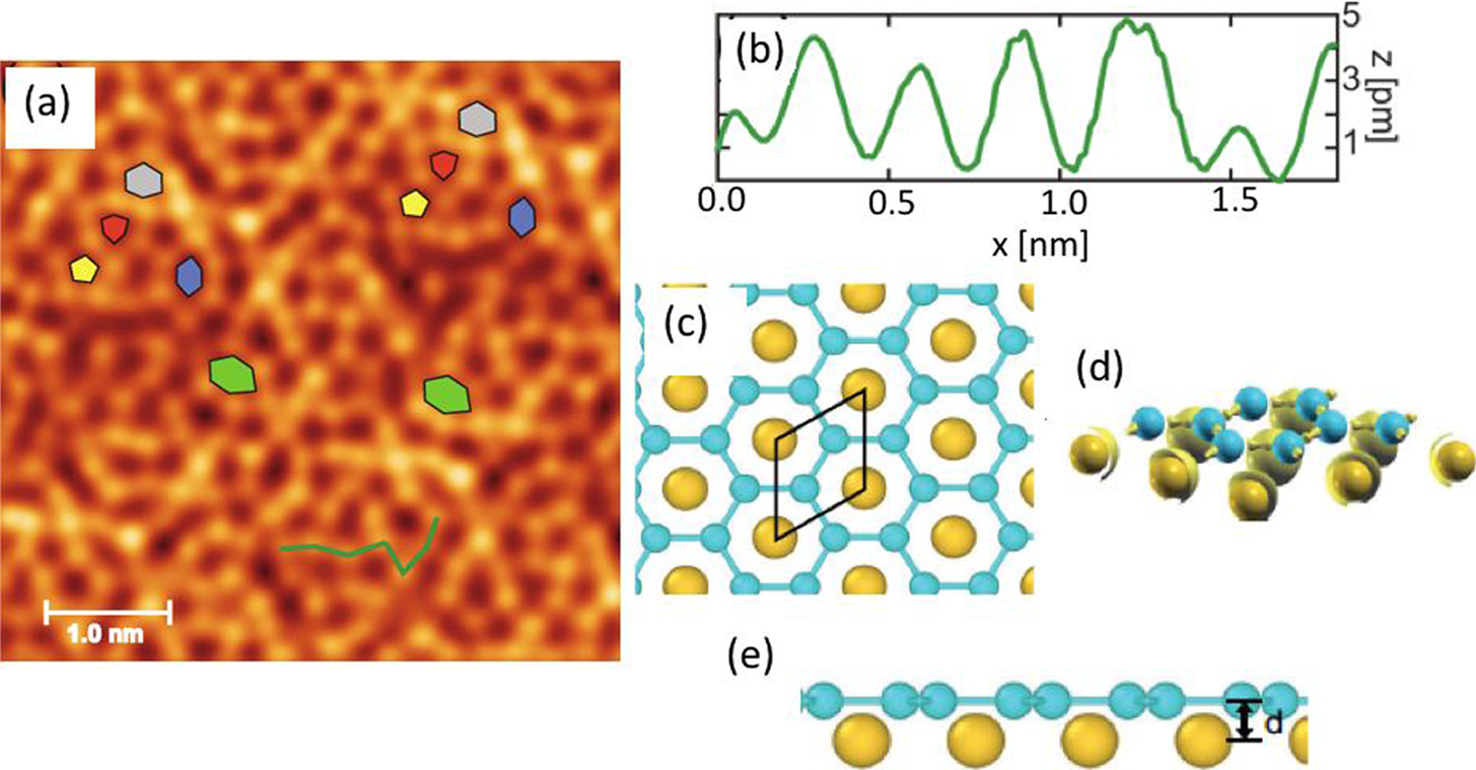
The dynamical stability of the system is confirmed by the calculated phonon spectra, shown in Figure 4. The imaginary frequencies initially shown in the spectra of the free-standing planar silicene reported in Ref. 58 are, instead here, much lower, owing to the suppression of the pseudo-Jahn -Teller distortion.
72
Moreover, their presence near the Γ point indicate that large area planar silicene may exhibit long-range deformation, which in turn explains the nature of domain-boundary-like features, visible in the STM topography.
4
Calculated phonon dispersion curve for the flat silicene/Au(111). Adapted from Figure 3 of Ref. 4, Copyright © 2019 WILEY-VCH Verlag GmbH & Co. KGaA, Weinheim, CCC Right link.
It is worth noting that the same system has been synthesized on Au(111) and studied with bond-resolved CO-functionalized STM tip, 73 revealing its fully planar character. Similar, albeit strongly strained (∼7%÷8 %), silicene layer has also been synthesized on Au(111) deposited on mica 74 The Raman spectroscopy, performed on such samples, also confirms almost flat silicene layer. 74
Silicene and multilayer silicene on Bi/Si(111)
Bismuth atoms on Si(111)7 × 7 surface adopt the ubiquitous √3 × √3 reconstruction.75–92 Depending mainly on the substrate temperature during the Bi/Si interface formation, and atomic Bi coverage that the so-called α-phase is achieved at ∼340°C with Bi coverage of 1/3 ML; the β-phase came out at 250°C at a Bi coverage of 1 ML; and the honeycomb phase matched at 2/3 ML of Bi was achieved at the temperature range 25°C < T <250°C, and believed to be, more probably, as a combination of α and β phases.75–92 These three structures can occur on Si(111)√3 × √3R30°-Bi, for short Si(111)√3 × √3-Bi, with different number of Bi atoms in the surface √3 × √3 unit cell, such as 1, 2 or 3 Bi, respectively.75–92
In a recent paper, 9 on one monolayer (1 ML) and 5-ML of Si films were grown on the α-phase Si(111)√3 × √3R30°-Bi, keeping the substrate at temperature around of 200°C, and studied by several measurement techniques, such as, REELS, AES, as a function of the electron beam incidence angle α, LEED, GIXRD, STM and STS. Interestingly, all results proved the synthesis of silicene and multilater silicene on this template Si(111)√3 × √3R30°-Bi. REELS spectra, at the Si K absorption edge (∼1.840 KeV), revealing the presence of two distinct loss structures attributed to transitions 1s→π* and 1s→σ*, attested the sp2-like hybridization of the silicon valence orbitals in both thin and thick Si films. The LEED patterns and AES spectra, exhibited the synthesis of a silicon allotrope on the α-phase of Si(111)√3 × √3R30°-Bi substrate, whereas the GIXRD measurements demonstrated a Si stack of 3.099 (3) Å with a √3 × √3 unit cell of 6.474 Å, typically observed in the synthesis of multilayer silicene.8–15,65 Indeed, STM and STS measurements, as well as DFT calculations, validated these findings. 65
Figure 5 reports the LEED patterns obtained on the different interfaces: (a) is the Si(111)7 × 7 (a); (b) Si(111)√3 × √3R30°-Bi; (c) 1 ML Si/Si(111)√3 × √3R30°-Bi, and (d) 5 ML Si/Si(111)√3 × √3R30°-Bi. In Figure 5(a), the typical diffraction pattern of the Si(111)7 × 7 reconstructed surface shows the large red rhombus, which represents the unit cell of unreconstructed Si(111)1 × 1, and the smaller pink rhombus is the unit cell of the Si(111)7 × 7 reconstruction, where the integer orders of (0, 1) of bulk silicon, and (n/7) spots of its 7 × 7 reconstruction are indicated. The LEED patterns of (c), and (d) of Figure 5, collected after the formation of the Bi α-phase on Si, 1 ML and 5 ML of silicene synthesis, manifest all the √3 × √3R30° reconstruction, where the blue, yellow and orange rhombus are related to each surface deposition.
9
LEED patterns collected on: (a) Si(111)7 × 7; (b) Si(111) √3 × √3R30°-Bi; (c) 1 ML Si/Si(111)√3 × √3R30°-Bi; and (d) 5 ML Si/Si(111)√3 × √3R30°-Bi. The patterns were acquired at primary energy of 33.3 eV, 29.3 eV, and 27.1 eV. The red rhombus in (a) is the 1 × 1 unit cell of Si(111); the smaller pink unit cell is the 7 × 7-Si surface reconstruction, the (0, 1) vertex, and that of the (6/7) spot are evidenced by the red and pink circles, respectively. The pattern in (b) shows the Si(111)√3 × √3R30°-Bi unit cell in blue, where the (1/3, 1/3) spot is indicated by the blue circle. The LEED pattern after the deposition of 1 ML of silicene (c), evidences two unit cells, represented by the yellow and blue rhombus, where the larger, yellow one, is related to silicene, and the blue one to Bi, respectively. In panel (d), the unit cell of 5 MLs of Si is marked with the orange rhombus. The GIXRD experimental setup is reported in (e), where θi = θr are the incident and reflected scattering angles; α is the in-plane tilt; ψ is the out-of-plane tilt. The comparison between the GIXRD pattern (black squares) collected from 5 MLs of Si on Si(111)√3 × √3-Bi interface (black line, offset of ψ = 2.0° offset), and the XRD pattern collected without offset (blue dots) is reported in (f). The red line is a least square Gaussian fit. Adapted from Figure 2, 8, and 10 of Ref. 9, Materials 2022, 15, 1730 https://doi.org/10.3390/ma15051730, by Gargnani et al., Copyright © 2022 by the authors. Licensee MDPI, Basel, Switzerland. This article is an open access article distributed under the terms and conditions of the Creative Commons Attribution (CC BY) license (https://creativecommons.org/licenses/by/4.0/).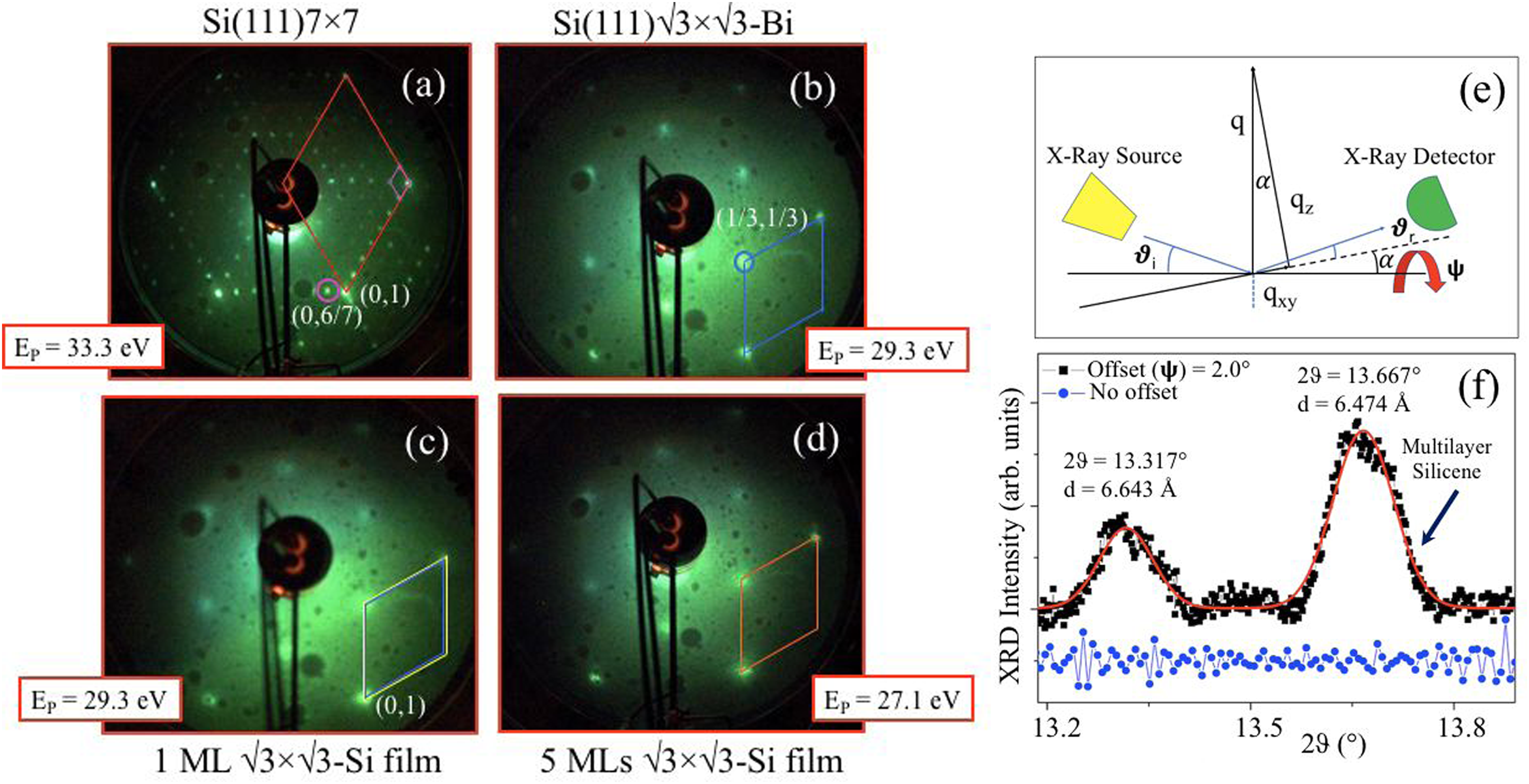
The two √3 × √3 unit cells of silicene and Bi, the yellow and the blue rhombus of Figure 5(c), have different dimensions, whereas the orange √3 × √3 (5 ML silicene stacks) in Figure 5(d) was not appreciably diverse from the yellow one of 1 ML of silicene. The deposited silicon atoms on the Bi, lay on top of the bismuth interface, conserving the same √3 × √3 reconstruction, and assuming a unit cell side greater than that of bismuth, in the reciprocal space. Thus, this comparison, in the reciprocal space, of the unit cell relative to 1 ML of silicene, yellow rhombus, (5 ML silicene) and that of bismuth (blue rhombus), shows an expansion of the 3.5%, giving a unit cell length of about 6.42 Å, in good agreement with silicene/multilayer silicene, grown on Ag(111) single crystal,8,10–13 and on the interface Si(111)√3 × √3-Ag.10,14,15
Figure 5(e) reports the GIXRD experimental setup, with the incident and reflected scattering angles, θi = θr; α angle is the in-plane tilt, whereas the ψ angle is the out-of-plane angle of tilt, applied to probe the in-plane lattice parameters, transferring part of the X-ray momentum along the surface.
Figure 5(f) shows the GIXRD pattern collected from 5 MLs of Si on Si(111)√3 × √3-Bi interface (black squares), with an offset of ψ = 2.0°, and the XRD pattern (blue dots) obtained at ψ = 0°, without offset, where the collected momentum along the z-direction only (blue line), no in-plane diffraction signal was observed. Extremely interesting, at ψ = 2.0° the in-plane reflections at 2θ = 13.317° (2) and 2θ = 13.667° (2) corresponding to the interplanar distances of d = 6.643 Å and d = 6.474 Å, unit cells of Bi-Si interface, and multilayer silicene, respectively, in very good agreement with LEED results. 9
The structural properties of the samples were investigated by means of the XRD experiments. Figure 6(a) illustrates the XRD patter from 4 MLs of silicon deposited on the √3 × √3R30° β-phase of Bi/Si(111) interface, 66 while, the inset reports the GIXRD pattern collected from the same Si/Bi interface, 4 MLs of Si on the β-phase Si(111) √3 × √3R30°-Bi interface, at α = 1.50°, and ψ = 2.0° offset out-of-the-plane (the GIXRD geometry is illustrated in Figure 5(e)).
Two important features can be drawn from Figure 6. The first is provided by the XRD pattern. In fact, it is worth noting that this XRD pattern was achieved performing a Si(111) rocking curve, in order to identify the appearance of a new contribution, due to the Si film, in addition to that of Si substrate. A single broad XRD peak was detected at 2θ = 28.445° (2), and attributed to (111) reflection of the [111] planes of the Si substrate, overlapped to the stacked layers of the Si film,
66
producing, by applying the Bragg law, for Si substrate and Si film a distance dSi(111) = 3.140 Å (5), in good accordance with values found for silicon substrate.8,10,14,15 XRD pattern from 4 MLs of silicon deposited on the √3 × √3R30° β-phase of Bi/Si(111) interface. The inset reports the GIXRD pattern collected from the same Si/Bi interface, 4 MLs of Si on the β-phase Si(111) √3 × √3R30°-Bi interface, at α = 1.50°, and ψ = 2.0° offset out-of-the-plane. Adapted from Figure 2 of Ref. 66 (Microstructures 2024: 2024019. DOI: 10.25/Microstructures 2023.74, by De Padova et al., Copyright © The Author(s) 2024. Open Access This article is licensed under a Creative Commons Attribution 4.0 International License (https://creativecommons.org/licenses/by/4.0/).
The second important point concerns the GIXRD pattern reported in the inset of Figure 5(a), which gives a unique in-plane lattice parameter of d = 6.61 (3) Å, for Si (111)√3 × √3, Si (111)√3 × √3-Bi β-phase, and 4 MLs of Si on the β-phase Si(111)√3 × √3-Bi interface,65,66 demonstrating that the Si film is not silicene multilayer, but, constituted, in this case, by stacks of tetragonal Si layers, in good agreement with DFT calculations. 65
These important findings were confirmed by the STM measurements,
66
shown in Figure 7, where are illustrated the filled-states image, collected on ∼ 0.27 ML of Si deposited at ∼ 220°C on Si (111)√3 × √3-Bi β-phase and its height profile.
66
(a) Room temperature STM image (71.5 × 70.2) nm2 (sample bias of – 3.0 V; I = 100 pA) from ∼0.27 ML of Si deposited at ∼ 220°C on the β-phase Si (111)√3 × √3-Bi; two arrows indicate two of the 2D Si islands; (b) height profile traced in, (a), along the blue line. In, (b), the blue and red triangles mark the positions of the height of the Si island, and the Si(111) substrate step height with √3 × √3-Bi β-phase. Adapted from Figure 3 of Ref. 66. (Microstructures 2024: 2024019. DOI: 10.25/Microstructures 2023.74, by De Padova et al. Copyright © The Author(s) 2024. Open Access This article is licensed under a Creative Commons Attribution 4.0 International License (https://creativecommons.org/licenses/by/4.0/).
Numerous distinct Si islands, equally distributed, with diameters between 3 and 5 nm, are visible in Figure 7(a) above the substrate terraces (looking brighter on the left, indicated by the two dark arrows, as an example, and darker on the right), after the deposition of Si on top of β-phase Si (111)√3 × √3-Bi substrate. These Si islands are mainly regular and very flat, as attested by the line profile reported in Figure 7(b), where the blue line crosses the two silicon terraces, and several Si islands (marked by the red and blue triangles). On both terraces, an average Si island height of 0.32 ± 0.03 nm, and a Si(111) step height of 0.33 ± 0.03 nm were found in good agreement, for the first case, to X-ray diffraction measurements, and, in the second, with the Si(111) atomic step. 93
Interestingly, in addition, all Si islands are commensurate with the Si(111) substrate, and Bi/Si(111), evidencing a √3 × √3 superstructure for both substrate and Si islands with a lattice unit length of 0.68 ± 0.04 nm, 66 in close agreement with GIXRD results reported in Figure 6.
Conclusions and perspectives
This review is focused on the first synthesis of silicene, buckled silicene, flat silicene, multilayer silicene on Ag(111), Au(111), α-phase and β-phase Si(111)√3×√3R30°-Bi, 2D silicon, as well as phosphorene on Au(111), and Te/Au(111). STM and first principles DFT calculations are reported, comparing the silicene phases, with single layer of blue phosphorus structures.
The two different atomic structures of multilayer silicene and 2D ordinary silicon were compared, by performing the Si growth on the two different templates that Bi atoms form on the Si(111) substrate: the α- and β-phases of Si(111)√3 × √3R30°-Bi. Auger electron spectroscopy, grazing-incidence X-ray diffraction, low/high electron energy diffraction, reflection electron energy loss, and scanning tunnelling microscopy, as well as spectroscopy, unambiguously demonstrated these two allotropic structures that adopt silicon, using these two phases of bismuth atoms on Si(111).
The reported studies are notably interesting, thanks to their unique structural, and electronic properties. Therefore, these two-dimensional materials could play a primary role for their potential applications in the fields of new flexible electronics, including the realms of optoelectronics, and solar cell devices.
Footnotes
Funding
The authors received no financial support for the research, authorship, and/or publication of this article.
Declaration of conflicting interests
The authors declared no potential conflicts of interest with respect to the research, authorship, and/or publication of this article.