
Abstract
Pd+ ions (90 keV) were implanted at normal incidence and at room temperature in different highly insulating (>200 GΩ) thermoplastic polymers (poly(methyl methacrylate), polypropylene, polyethylene terephthalate glycol-modified, and polycarbonate). At high fluence and optimized process parameters, the ion implantation gives rise to the formation of a nanocomposite thin surface layer constituted by Pd nanoclusters and carbonaceous material (nanographite/amorphous carbon). The morphological, microstructural, and microanalytical properties of the nanocomposite layers were investigated by He-ion microscopy, glancing incidence X-ray diffraction, and Raman scattering, respectively. The electrical properties were characterized by resistance, van der Pauw, and Hall measurements. We performed accurate simultaneous deformation/bending experiments and electrical resistance measurements. We show that the electrical resistance varies linearly with the mechanical deformation (beam deflection) applied. The experimental results are interpreted by “hopping conductivity” model considering the nanostructure configuration of the nanocomposite layers. A gauge factor in the range between 4 and 8, depending on the ion-implanted polymer, was obtained for prototype strain gauge devices.
Keywords
Introduction
In the last decades, ion beam irradiation attracts an increased attention due to the possibility to modify the surface structure and the electronic properties of insulating polymers. Of particular, scientific and technological interest are ion bombardments at low energy (range from few keV to about 200 keV) and at high fluences in the range 1016–1017 cm−2. 1,2 The projected range of low energy ions involves a shallow surface region and thin surface layer of the implanted polymer.
The ion implantation in polymers, the molecular modification, and rearrangement of the atomic species in the ion-bombarded polymer region are complex processes that depend, besides the ion energy and fluence, on the ion species and the polymer parameters, its molecular structure, and elemental composition. 3 –5 The energy transfer of energetic ions to the target polymer causes structural damage and chemical modification that implies the formation of hydrogen and free radicals (carbon) and, depending on the polymer type, also oxygen. The created species may be involved in other reactions that generally include cross-linking and scission of polymer chains and gas evolution. 3,4,6 The implantation-induced damage and chemical modification depend on the ion energy and mass, while the extent of the damage depends on the fluence. Many insulating polymers were observed that a chemical modification seems more important in the fluence range between 1012 cm−2 and 10 14 cm−2 and depends on the ion species implanted, while a fluence above 1015 cm−2 generates structural defects and leads to the formation of carbonaceous materials. 2,3,7
Furthermore, implantation of ion metals in insulating polymers is an effective method to produce metallic or metal-oxide nanoparticles in polymers and to modify the polymer structure giving rise to the formation of novel polymer nanocomposites. At high fluences, the nucleation of nanoparticles may occur due to the high metal cohesive energy and the low metal–polymer interaction energy. The growth of metal or metal-oxide clusters is affected by various factors and parameters, such as density and mobility of the implanted metal atoms, and composition and molecular structure of the target polymer. 7,8
In summary, metal-ion implantation at low energy and high fluence in insulating polymers may give rise to the concurrent formation of carbonaceous materials (amorphous carbon and nanographite) and metal or metal-oxide nanoparticles in the polymer matrix. Both the formation of amorphous carbon and carbonaceous materials and the metal nanoparticle formation modify the electronic transport properties significantly, and an increase of the conductivity can be observed. 3,4,7,9 –12 The realization of metal–carbon–polymer nanocomposite structures by metal-ion irradiation opens the door for potential applications in various technological fields such as electronics, magnetics, optoelectronics, optics, and mechanics but also applications in biological and medical fields may become feasible. 1,7 –9,13 –17 In addition, it should be noted that metal–carbon–polymer nanocomposite films may exhibit interesting pressure-sensitive, catalytic, and gas sensing properties and are promising candidates for the realization of efficient flex, catalytic, and gas sensor devices. 18 –21
In previous studies, we reported on low energy (60 keV) implantation of Cu+ and Ni+ ions in polycarbonate at fluence of 5 × 1016 cm−2 and 1 × 1017 cm−2. 14,22 The electrical resistance was reduced considerably and a dependence on the deformation, that is, mechanical-induced strain, was observed proving the potential application of these nanocomposite surface films for the fabrication of strain gauge devices. We also observed that for fluence ≥1 × 1017 cm−2, an increased structural damage and surface erosion occur that lead to an increase of the electrical resistance and compromise the structural stability of the near-surface nanocomposite film. This finding is in accordance with other experimental results. 23
In the present work, we report on the implantation of Pd+ ions in different polymers and analyze the electrical properties of the fabricated near-surface nanocomposite layers. In particular, we analyze in detail the electrical resistance variation as a function of the mechanical deformation (strain) induced by bending. The article is organized as follows: the “Experimental” section describes the polymer materials, the synthesis and process technologies, the characterization techniques, the evaluation methods for the functional properties, and the device characterization; in the section “Results and Discussion,” the morphological, nanostructural, and electrical properties are presented and the mechanical deformation and mechanoelectrical properties of the device structures are analyzed and discussed; the section “Conclusions and Perspectives” summarizes the main results and provides an outlook for further studies and device development. Additional and useful information and data are provided in the Supporting Information available on the SAGE journal website.
Experimental details—materials, synthesis, and characterization
Materials
The implantation of Pd+ ions was performed on various polymers to evaluate and analyze: (1) the different effect and damage of the ion-beam process on the polymer materials and (2) the formation of metal–polymer nanocomposites and their electrical properties. For the fabrication of the metal–polymer nanocomposites, the amorphous polymers poly(methyl methacrylate) (PMMA, C5H8O2), polypropylene (PP, C3H6), and polycarbonate (PC, C16H14O3), and the semicrystalline polymer polyethylene terephthalate glycol-modified (PETG, C10H8O4) were used. All the polymers (raw materials) were supplied by RS-components (https://www.rs-components.com/index.html) with the main characteristics (material density and tensile strength) summarized in Table 1. The materials were delivered as plates with sheets thickness of 3 mm. Rectangular samples of the same geometrical size (70 mm × 25 mm) were cut from the plates using a pantograph milling machine. It should be noted that all the polymers, with exception of PP, are composed of C, H, and O atoms; PP is constituted by C and H elements only, that is also emphasized by the lower mass density. The electrical characterization of the pristine polymers was measured with a programmable electrometer (Instruments, Solon (Ohio), USA) with maximum range up to 200 GΩ. For all the polymers, no electrical resistivity could be measured concluding that the samples are insulators having a resistivity R > 200 GΩ.
Characteristics of the polymers used for the ion implantation.
PMMA: poly(methyl methacrylate); PP: polypropylene; PC: polycarbonate; PETG: polyethylene terephthalate glycol-modified.
Synthesis and process technologies
The ion implantation was performed by using a high-current ion implanter (Danfysik Model 1090, Taastrup, Denmark) optimized for surface modifications. All the polymer samples were implanted by using the same process parameters, keeping the ion-beam energy at 90 keV and the beam current density at about 120 nA cm−2. During the ion-beam irradiation, a rotation of sample and a vertical sweeping of the ion beam were performed to minimize surface charging and surface overheating. For this purpose, we also used an Al-foil as a mask (size: 40 mm × 18 mm) placed on the surface of the polymer plate. The ion-beam dose was in the range between 5 × 10¹⁵ Pd+ ions cm−2 and 1 × 10¹⁷ Pd+ ions cm−2. Here, we will consider and discuss only the results obtained for samples with dose 5 × 10¹⁶ Pd+ ions cm−2, while samples fabricated with lower and higher ion dose did not exhibit the necessary and suitable functional properties (electrical conductance). It should be also noted that the choice to use the ion-beam energy of 90 keV represents a compromise to obtain an embedded electrically conductive nanofilm. Preliminary experiments with lower (50 keV) and higher ion energy (180 keV) yield unsatisfactory results: at lower ion energy, the nanofilm was less stable from a mechanical and chemical point of view, while at higher energy, it was necessary to increase the ion-beam dose to obtain an electrically conductive nanofilm. Consequently, an enhanced radiation damage occurred, which was detrimental to the electrical properties of the nanocomposite film.
Ion implantation parameters of Pd+ ions such as projected range and in-depth (longitudinal) straggling were determined and analyzed by Monte–Carlo simulations and transport of ions in matter (TRIM) calculations using the stopping and range of ions in solids (SRIM) 2013 codes. 24 The projected range and straggling as well as the energy loss due to the energy transfer of the incident Pd+ ions are summarized in Table 2. The energy transfer of incident energetic ions to a solid medium occurs mainly via both electronic and nuclear energy loss processes; in the first case, the ions transfer their energy to electrons that yield ionization and excitation processes, while the second process causes displacement of the matrix atoms creating vacancies and phonons. Both processes cause irradiation damage in the polymer and favor mainly cross-linking and chain scissioning. 5,25
Ion-projected range (peak maximum of the Pd+ ions depth distribution), in-depth straggling (depth distribution width), and energy loss percentage of the 90 keV Pd+ ions for the polymers considered.

PMMA: poly(methyl methacrylate); PP: polypropylene; PC: polycarbonate; PETG: polyethylene terephthalate glycol-modified.
The calculated parameters regarding the peak maximum of the depth distribution of the implanted Pd+ ions range from 68.5 nm (PMMA) to 96.5 nm (PP), while the depth distribution width ranges between 14 nm and 17 nm. The energy loss data obtained from TRIM calculations show that about 55% of the total incident energy is transferred through nuclear processes (about 45% through electronic process) in PMMA, PETG, and PC. For PP, we obtain almost the same contribution of energy loss (∼50%) through electronic and nuclear processes.
Characterizations
The surface morphology of the Pd+ ion-implanted polymer samples was analyzed by using a Helium-ion microscope (HeIM, Zeiss Orion Plus, Jena, Germany) with a minimum He+-ion beam size of 0.35 nm. All the observations were made with an acceleration voltage of 25 kV, while the working distance and sample tilt angle for all the observations were kept equal to 11.6 mm and 10°, respectively.
Glancing-incidence X-ray diffraction (GIXRD) and Raman scattering experiments were carried out for microstructural and microanalytical characterization of the ion-implanted near-surface nanocomposite layers. For the X-ray diffraction measurements (X-ray wavelength = 0.154 nm), the multipurpose diffractometer Empyrean (Malvern Panalytical: Malvern, UK) in the thin-film setup configuration, equipped with a multilayer-X-ray mirror as monochromator–collimator, was used. To reduce the background/fluorescence scattering, a parallel-beam-plate collimator and graphite crystal monochromator were placed in front of the scintillation detector. All the GIXRD measurements were carried out with a fixed incidence angle of 1.0° between X-ray beam and sample surface, and 2θ scans were recorded with a step resolution of 0.02° in the angular range between 5° and 85°.
The Raman scattering experiments were carried out at room temperature (RT) by using the LabRAM HR Evolution Raman spectrometer (Horiba Scientific, Horiba Ltd: Kyoto, Japan). The excitation wavelength used for all the Raman measurements was 633 nm (laser excitation energy 1.96 eV).
The electrical resistivity and Hall coefficient measurements were carried out at RT by using the HL5500PC (BIO-RAD, Hercules (CA), USA) apparatus. This instrument performs the measurements by the Van der Pauw method employing the four-point probe. The four electrical contacts, placed at the perimeter of the samples, were made by using a silver conductive paste (Locite EDAG 915, Henkel, Düsseldorf, Germany).
Functional properties and device characterization
For the electrical resistance under elastic deformation (mechanical stress), specific electrical contacts along the shorter edges of the ion-implanted area were made by using the silver conductive paste (Henkel) to assure parallel flux lines of the measured electrical current among the two electrodes (x-axis, see Figure 1(a)).

The scheme of the ion-implanted specimen (a) with the geometrical parameters L = 70 mm, b = 25 mm, h = 3 mm, d = 40 mm, and w = 18 mm; the electrical resistance was measured during elastic deformation (along the z-axis) between the electrodes (along the x-axis). The mechanical elastic deformation along the z-axis (b) was obtained by applying a force F at the free specimen end of the polymer plate (conveniently, the values of force F are taken positive for case A and negative for case B).
The equipment for the mechanical deformation (MTS System Corporation, Eden Prairie, Minnesota (USA) model Alliance RT 50 kN) with a 2 kN cell (class 0.5 ISO7500 -1) was used, while the electrical measurements (resistance) were measured with multimeters HP 3458A and HP 6632A (Hewlett Packard, Palo Alto (CA), USA) having a maximum range of 1 GΩ. For mechanical elastic deformation, the samples were fixed by a clamp at one specimen end, while at the other end, a force F was applied to deform (bend) the specimen (Figure 1(b)). During these experiments, by applying the force F, the displacement s elongation at the free specimen end and the electrical resistance R were measured simultaneously.
Results and discussion
Morphological and nanostructural properties
The HeIM images of the ion-implanted polymer surfaces exhibit pronounced nanostructures that differ considerably depending on the polymer type (Figure 2). In general, a surface roughening is well-observed for all the polymer samples; the morphological details observed are in part also the result of the surface damage and polymer degradation due to the ion implantation and the correlated graphitization of the polymers. 2,7 In fact, due to the polymer-chain scissions caused by ion irradiation, a carbonization of the surface and Pd cluster formation may occur. H and O atoms, constituting the polymers, may mainly volatilize but may play a role in the formation of the nanocomposite surface layer, for example, formation of O-containing Pd clusters.
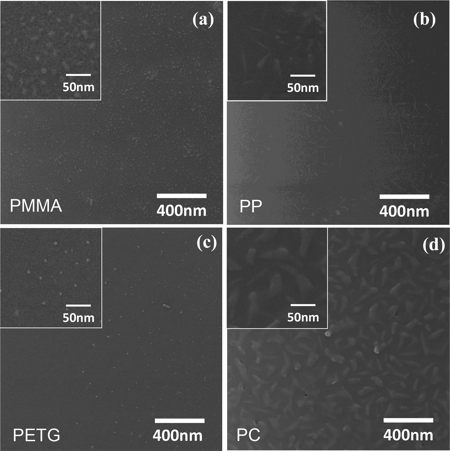
(a)–(d) HeIM images of the surface morphology of the Pd+-ion-implanted polymers. The insets show details of the nanostructures and the final composite surfaces. HeIM: helium-ion microscope.
For the chosen ion implantation parameters, we expect that no single isolated Pd clusters but highly dense clusters are formed giving rise to an almost homogeneous polycrystalline Pd nanofilm that is close to or embedded beneath the sample surface. Despite of the very low selected ion-beam current densities (∼120 nA cm−2), during the irradiation process sputtering effect are likely and they can affect ion-projected ranges with respect to the estimated ones. 26,27 The HeIM images show the surface morphology of the assembled nanocomposite film. The PMMA sample (Figure 2(a)) exhibits nanostructures of average size of about a 10 nm, while the nanostructures on the PP surface (Figure 2(b)) are elongated with average length and width of about 50 nm and 10 nm, respectively. The PETG surface seems relatively smooth and only isolated few nm large point-like structures are observed (Figure 2(c)). Contrary, the PC surface (Figure 2(d)) exhibits larger and mostly irregular morphological structures with average size between 50 nm and 150 nm. Besides, the size of the structures and contrast between the particles and the polymeric substrate suggests the co-occurrence of towering effects. Similar structures were already reported for high-fluence metal-ion implantation in viscous polymers. 28,29
The crystalline structure of the assembled nanofilms is investigated by GIXRD. For all the samples, we recorded GIXRD pattern prior and after ion implantation. The pristine polymers PMMA, PETG, and PC are amorphous and show the typical broad diffraction peaks. After ion implantation, these broad peaks are still the dominant diffraction features of the patterns. However, using the “difference method” (subtracting from the GIXRD pattern the reference pattern obtained from the pristine sample) fine and weak intensity changes in the diffraction patterns can be observed and analyzed.
Here, for simplicity sake, we show in Figure 3 only the results obtained for the PMMA polymer. The GIXRD patterns show, due to the amorphous polymer structure, three distinct and broad diffraction peaks in the 2θ angular range between 15° and 45°. However, the difference curve exhibits a diffraction peak at 2θ≈41° that can be attributed to the (111) Bragg peak of metallic Pd (Space Group Fm3 m) in accordance with International Centre for Diffraction Data (ICDD) cards # 00-087-0637 and # 00-087-0645). 30 This diffraction peak was also observed for all the other polymers investigated here. It is worth noting that a small angular shift of the (111) Bragg peak toward a smaller diffraction angle has been observed for all cases and can be interpreted by the possible presence of a small amount of substitutional oxygen atoms in the cubic Pd lattice. These findings are in agreement with XPS measurements that are not reported here but will be published in a forthcoming article. 31 The inset in Figure 3 shows the experimental (111) Pd Bragg peak together with the Voigt peak fitting. By using Scherrer’s equation, from the full-width-half-maximum (FWHM) of the diffraction peak, we determine a crystalline domain size of 2.5 nm. Similar results were obtained for PETG and PC, that is, crystalline domain size of 2.1 nm and 2.3 nm, respectively. The quantitative evaluation for PP is not straightforward being PP a semicrystalline polymer having several Bragg diffraction peaks overlapping the (111) Pd Bragg peak. The GIXRD results clearly demonstrate the formation of nanoparticulate Pd films, that is, Pd nanoparticles constituted by nanocrystalline domains.

GIXRD patterns before (pristine PMMA, red line) and after ion implantation (Pd+-ion-implanted PMMA, blue line); intentionally, the two patterns are slightly displaced along the y-axis. The difference curve (black line) exhibits the (111)Pd peak also shown in the inset together with the Voigt-fit for the determination of the crystalline domain size. GIXRD: glancing-incidence X-ray diffraction; PMMA: poly(methyl methacrylate).
Raman spectroscopy is a powerful tool to monitor and analyze the chemical and structural properties of polymers 32 and their modification due to ion irradiation. 33 –38 The Raman scattering measurements at RT prior and after ion implantation show the chemical and microstructural surface modification of the polymers (Figure 4). The Raman spectra of the pristine polymers (blue lines in Figure 4) exhibit the characteristic peaks and their positions correspond to the vibrations as indicated in the labelling and are in accordance with the data reported in the literature. 33 –39 Here, the Raman spectra of the PC are not shown because the characteristic peaks are not visible due to a strong luminescence probably caused by additives that may cover the characteristic PC Raman signal. 40 Indeed, in commercial PC that is employed for its transparency and optical properties, UV stabilizers are frequently used to prevent autoxidation and to suppress discoloration. 41
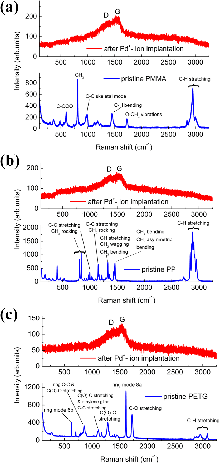
Raman spectra at RT prior (blue line) and after (red line) 90 keV Pd+ ion implantation in PMMA (a), PP (b), and PETG (c) polymers. The spectra after ion implantation exhibit the characteristic D and G bands associated to the carbonization process due to ion irradiation. PMMA: poly(methyl methacrylate); PP: polypropylene; PETG: polyethylene terephthalate glycol-modified; RT: room temperature.
After ion implantation, all the characteristic Raman peaks of the polymers disappear and two broad bands are observed that confirm the formation of cross-linked carbon network on the polymer surface (red lines in Figure 4). The two bands, labelled D and G, are located approximately at frequency 1360 cm−1 and 1545 cm−1, respectively and indicate C–C bond breaking, chain scissioning, and formation of carbon radicals. 34,23 The two broad peaks are associated to amorphous/nanocrystalline carbon: the peak at 1360 cm−1 corresponds to the breathing mode of sp2 atoms in rings only and appears due to disorder (D peak), the peak at 1545 cm−1 corresponds to the bond stretching vibrations of all pairs of sp 2 atoms in aromatic rings as well as chains and is known as the graphite peak (G peak). 41,42 Figure 5 shows the D and G Raman peaks together with Lorentzian peak fits to determine the exact peak parameters. The determined values of peak positions, relative peak heights, peak widths, and areas are summarized in Table 3.
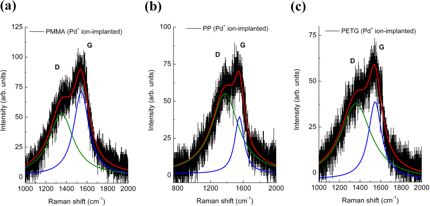
Line fitting of the D and G Raman bands of PMMA (a), PP (b), and PETG (c). The relative peak intensity of bands D (green line) and G (blue line) changes for the three polymers. PMMA: poly(methyl methacrylate); PP: polypropylene; PETG: polyethylene terephthalate glycol-modified.
Raman shift, intensity, FWHM, and area of the D and G peaks as determined from the Lorentzian fit of the spectra in Figure 5.

PMMA: poly(methyl methacrylate); PP: polypropylene; PETG: polyethylene terephthalate glycol-modified; FWHM: full-width-half-maximum.
The peak position of the D and G bands suggests that from a structural point of view the carbonaceous layer is within stage 2 of the three-stage model proposed by Ferrari and Robertson, 43 that is, between nanocrystalline graphite and amorphous carbon. In fact, the position of the G peak is below 1580 nm−1 and an increased dispersion of the G band is observed, too. Here, the commonly used relations that consider the intensity ID /IG or area AD /AG ratios, for the determination of the nanocrystalline graphite domain size, 43,44 are not useful due to the coexistence of amorphous and nanocrystalline phases. We expect a crystal domain size <10 nm due to the generation of point defects and structural disordering by ion implantation. Instead, we use the FWHM (ωD ) of the D band as suggested in ref. 45 by applying the relation La = 580/ωD . We obtain the grain size of about 2.1 nm, 1.5 nm, and 2.3 nm for the PMMA, PP, and PETG samples, respectively. It is interesting to note that a higher graphite index value ID /IG (AD /AG ) for PP is observed, indicating an increase of sp2 C–C bonding. This finding is consistent with the fact that higher electronic stopping power (Table 2) promotes the formation of free radicals leading to cross-linking and conjugation that favors the formation of C–C bonding and carbon-rich structure. 7,25
X-ray diffraction and Raman scattering results indicate that Pd+-ion implantation in polymers generate a nanocomposite thin layer, about 100 nm thick, constituted by metallic Pd nanoclusters embedded in a carbonaceous layer constituted by graphitic nanoclusters and amorphous carbon. The crystalline domains size of the Pd and graphitic nanoclusters is in the order of about 2.5 and 2.0 nm, respectively. The shallow nanocomposite films are formed on the polymer surface and well adhere to the polymer matrix. This finding is also corroborated by extensive and detailed microanalytical investigations (not shown here) using X-ray photoelectron spectroscopy measurements and field-emission electron microscopy observations that will be presented in a forthcoming article. 31
Electrical properties
The electrical resistance measurements carried out at RT and without applying any deformation or pressure on the polymer plates yield the following R0 values of the ion-implanted polymers: 4.31 MΩ, 1.64 MΩ, 29.2 kΩ, and 255 kΩ for PMMA, PETG, PP, and PC polymers, respectively. The electrical resistivity (R0 ) of the Pd+-ion-implanted samples, without any special surface protection and preserved in a closed box, remained very stable over time and also after 14 months, only a 20% reduction of the electrical resistivity values was measured.
Electrical properties, such as sheet resistance, surface charge density, Hall, and majority carrier density, were measured by van der Pauw method on the ion-implanted samples. The experimental data are summarized in Table 4. The highest sheet resistance, surface charge density, and Hall mobility were obtained for PMMA, while the highest majority carrier density has been achieved for PP. The lowest Hall mobility was measured for PC. It is worth noting that the majority carriers for PP and PC are electrons, while for PMMA and PETG are holes. The reason for this finding is not clear and well-understood, but it is certainly correlated with the defect structures, hydrogenation, and bonding in the nanostructured Pd nanocluster—carbonaceous nanofilm. The different electrical properties for these polymers that have been ion-implanted by using the same process conditions indicate that the specific molecular structures and the ion irradiation damages play a crucial role in the metal-carbonaceous nanocomposite formation and their physical properties.
Electrical properties (sheet resistance, surface charge density, Hall coefficient, and majority carrier density of the ion-implanted polymers (nanocomposite surface layer).
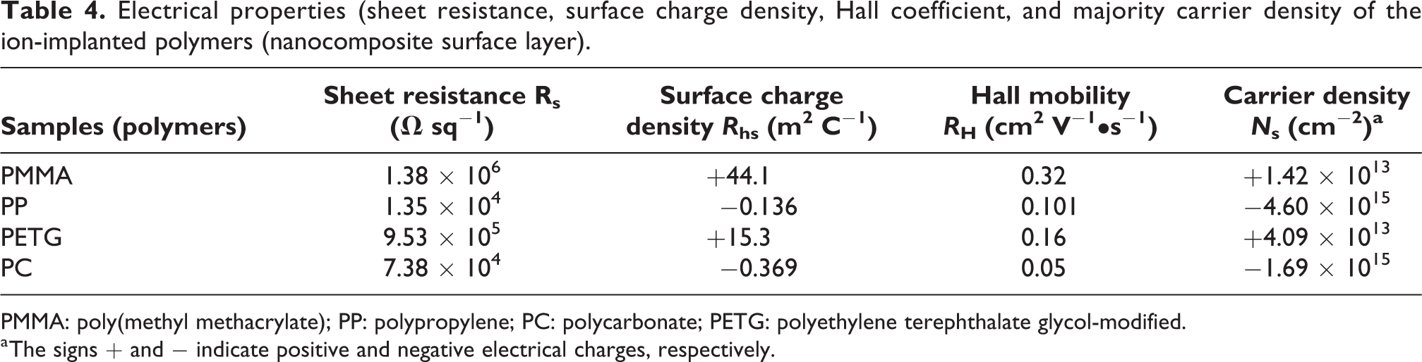
PMMA: poly(methyl methacrylate); PP: polypropylene; PC: polycarbonate; PETG: polyethylene terephthalate glycol-modified.
a The signs + and − indicate positive and negative electrical charges, respectively.
Mechanical deformation and mechanoelectrical properties
The thin ion-implanted polymer slabs were mechanically deformed as shown schematically in Figure 1(b). The slabs are fixed at one end and a force F is applied at the other end; the force is applied in both directions, down (A) and up (B), resulting in a tensile and compressive deformation, respectively, of the embedded ion-implanted nanofilm. The deviation of the slab (along the z-axis, see Figure 1) shows a linear relationship with applied force F (see Figure S2 of the Supporting Information). For all the samples, a maximum force F of ±6 N was applied and the corresponding deviation s was measured. The greatest slab bending (deviation s) was measured for PP, but at the same time for F>5 N, a slight deviation from a linear relationship can be noticed. The slope of function F(s), that is,
Slope of the linear interpolation functions for the relations force deviation F(s) and relative electrical resistivity—strain, δr (∊), that is, fs and r∊ , respectively.
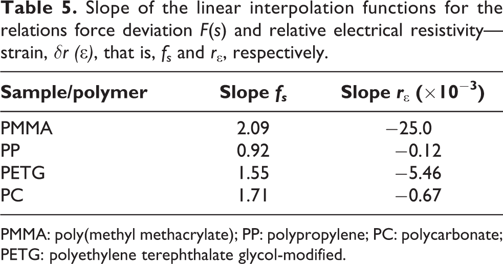
PMMA: poly(methyl methacrylate); PP: polypropylene; PC: polycarbonate; PETG: polyethylene terephthalate glycol-modified.
The electrical resistance Rs
of the ion-implanted nanofilms under deformation is measured simultaneously with the deviation s, beam deflection, along the z-axis (see Figure S3 of the Supporting Information). An almost linear relationship between electrical resistivity and slab bending (deviation s) is observed for all samples considered here (Supporting Information, Figure S2). The slab bending causes a strain, ∊, in the ion-implanted layer due to the surface layer elongation (tensile strain) and contraction (compressive strain) along the x-axis. Figure 6 shows the relative electrical resistance variation difference, that is,

Relative electrical resistance as a function of the strain caused by the bending of the ion-implanted polymer slabs PMMA (black points), PP (red triangles), PETG (green points), and PC (blue triangles). A linear behavior is observed for all samples in both tensile and compressive strain states (experimental data points (dots) and linear fit (continuous line) as a guide to the eye). PMMA: poly(methyl methacrylate); PP: polypropylene; PC: polycarbonate; PETG: polyethylene terephthalate glycol-modified.
The electrical resistance variation in dependence of the slab bending (deviation s) can be explained by the stretching (tensile strain) and compression (compressive strain) along the axis x of the nanocomposite thin film during the sample bending as shown schematically in Figure 7. Considering that the nanocomposite thin layer is constituted by Pd nanoclusters embedded in a carbonaceous (nanographite and amorphous carbon) film (A in Figure 7), we can figure out that the intergrain (nanostructures) distance changes by bending, and the electrical resistivity variation can be explained by the hopping conductivity model for granular materials. 46 –48 The beam deflection (Figure 7) induces a compressive (compression) or tensile (stretching) strain, that is, the intergrain distance (B in Figure 7) is reduced and the electrical resistance decreases, or, under stretching the intergrain distance becomes larger and the electrical resistance increases (case C in Figure 7), respectively.
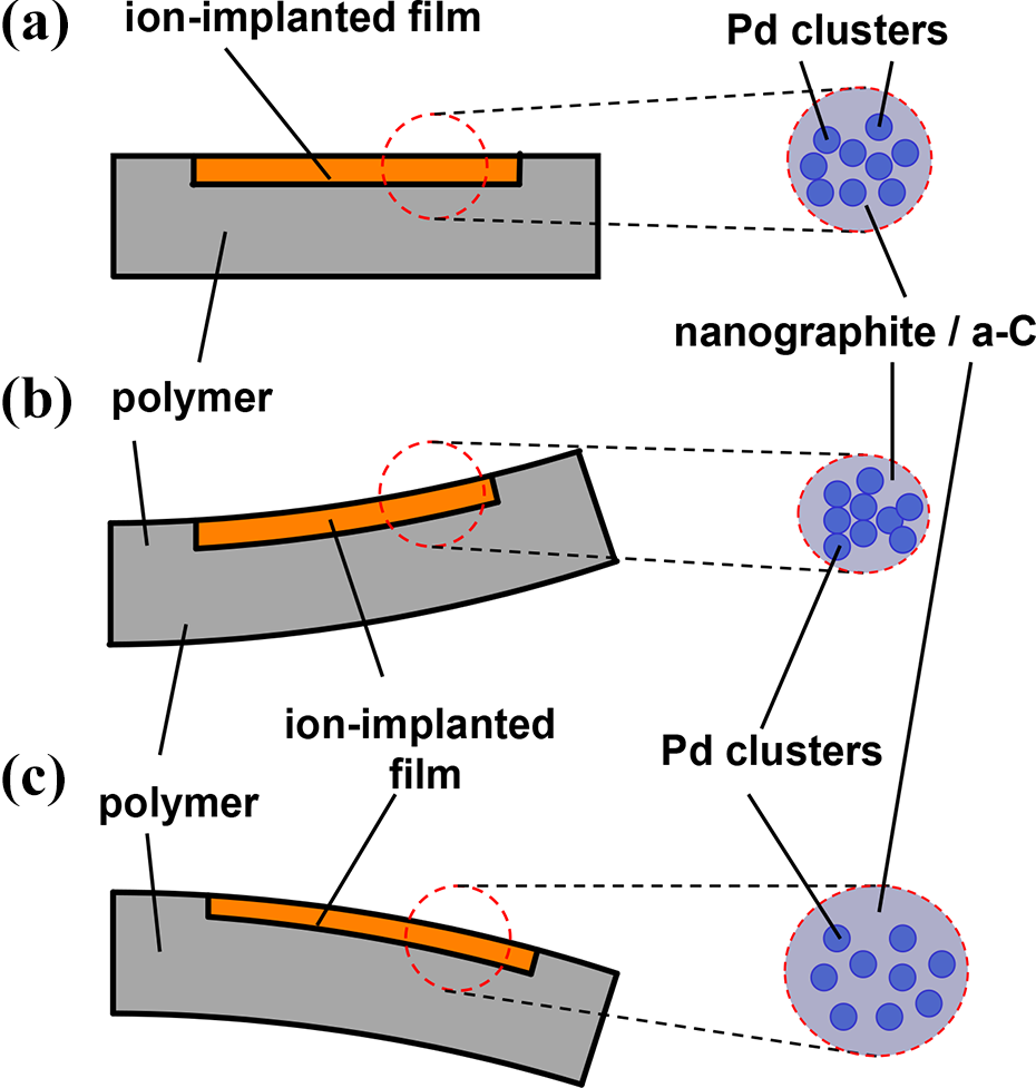
Schematic representation of the intergrain (nanocluster) distance variation in the Pd+ ion-implanted nanocomposite layer by bending of the sample, affecting, consequently, the electrical properties of the nanofilm: the Pd cluster intergrain distance is reduced (B) or increased (C) by compression or elongation, respectively, causing also accordingly a decrease (B) or an increase (C) of the electrical resistance with respect to situation of case A (undeformed layer).
To quantify and evaluate the sensing properties and to determine the gauge factor (GF) of the ion-implanted nanocomposite layers, we modeled and analyzed the layer shortening (compressive strain) or elongation (tensile strain), length change ±ΔL, as a function of the deviation s. 49 For this purpose, we calculated the length change ΔL on the sample surface as a function of deviation s (see Figure S1) as reported in Supporting Information. The GF is defined as the ratio of electrical resistance fractional change to length fractional change: GF = ΔR/ΔL. The obtained GF values of the ion-implanted polymer samples are summarized in Table 6.
GFs for the 90 keV Pd+-ion-implanted polymer deformation sensors.

PMMA: poly(methyl methacrylate); PP: polypropylene; PC: polycarbonate; PETG: polyethylene terephthalate glycol-modified; GF: gauge factor.
The highest GF value measured is for the polymer sample PMMA, however, for all the polymer samples considered here, a GF factor larger than 2, that is, the typical value for metallic strain gauges 18,48 was obtained.
Conclusions and perspectives
We investigated the ion implantation of 90 keV Pd+ in different insulating thermoplastic polymers such as PMMA, PP, PETG, and PC. The results show that a thin surface layer, constituted by Pd nanoclusters embedded in a nanographite/amorphous carbon matrix, is formed. The Pd carbonaceous nanocomposite layer is stable in time (no significant deterioration is observed after 15 months), is robust from a structural point of view, and adheres well on the polymer surface. The electrical properties of the nanocomposite films depend on the chemical structure of the thermoplastics, but independently of the polymer, an increase of the electrical conductivity has been obtained.
The electrical resistance varies with the mechanical deformation, applying a tensile or compressive strain that makes these structures suitable as strain gauge devices. The mechanoelectrical behavior of the device structure can be explained and understood by a hopping conductivity model based on the granular structure and nanostructural configuration of the material. For the realized samples, GFs between 4.3 and 7.7, depending on the polymer, have been found.
Based on our findings, we believe that further improvements of the strain gauge properties and device performances could be achieved. For example, investigations of the ion-implanted nanocomposite films should be also focused on the layer structure, considering a serpentine (zigzags) surface structure or interdigital electrodes, 48 that may increase the GF. Additional experiments and studies should be also focused on process technologies regarding the electrode fabrication and the encapsulation of the surface nanocomposite layer to ensure an environmental protection of the film device.
Supplemental material
Supplemental Material, NAX-20-0037_-_Supplemental_Material - Strain gauge properties of Pd+-ion-implanted polymer
Supplemental Material, NAX-20-0037_-_Supplemental_Material for Strain gauge properties of Pd+-ion-implanted polymer by Francesca Di Benedetto, Ciro Esposito, Maria Lucia Protopapa, Emanuela Piscopiello, Marcello Massaro, Gennaro Cassano, Valentino Filiberto, Martino Palmisano and Leander Tapfer in Nanomaterials and Nanotechnology
Footnotes
Author’s note
This article is dedicated to the memory of our wonderful colleague, Dr Emanuela Piscopiello, who passed away prematurely at the final stage of this research.
Declaration of conflicting interests
The author(s) declared no potential conflicts of interest with respect to the research, authorship, and/or publication of this article.
Funding
The author(s) received no financial support for the research, authorship, and/or publication of this article.
Supplemental material
Supplemental material for this article is available online.
References
Supplementary Material
Please find the following supplemental material available below.
For Open Access articles published under a Creative Commons License, all supplemental material carries the same license as the article it is associated with.
For non-Open Access articles published, all supplemental material carries a non-exclusive license, and permission requests for re-use of supplemental material or any part of supplemental material shall be sent directly to the copyright owner as specified in the copyright notice associated with the article.