
Abstract
In this article, a wideband, polarization-insensitive, and wide-incident-angle stable absorber based on conductive ink frequency selective surface is presented. The presented absorber is compatible with screen printing technology. The design and absorption principle of the proposed absorber is presented, and simulation analysis is conducted. The simulation results show that in the frequency range 6.58–16.38 GHz, the absorptivity of the proposed absorber is greater than 90%, while the relative absorption bandwidth is 85.4%. The whole absorber structure is relatively thin, having a total thickness of 3.3 mm, corresponding to 0.126λ0 at its center frequency. In addition, for both transverse electric and transverse magnetic incident waves, the proposed absorber achieves the absorptivity of more than 80% at the incident angle of up to 45°. A prototype of the proposed absorber is fabricated and used in experimental verification. The obtained experimental results show a good agreement with the numerical simulations. This absorber has great potential applications in the field of microwave sensing and absorbing.
Introduction
Electromagnetic (EM) wave absorber, as an invaluable component which has been widely used in energy harvesting and stealth systems, has attracted intense scientific attention. 1 –3 Recently, several artificial structures, including frequency selective surfaces (FSSs) and metasurfaces, have been used to fabricate EM wave absorbers. 4 –6 Due to the artificial surface-based EM absorber has the advantages of flexible design 7,8 and adjustable response, various structures have been designed. Besides, absorbers based on artificial surfaces can achieve ultra-wide bandwidth 9 –11 and extremely narrow bandwidth 12 through a well-designed structure, which has been widely used in stealth materials, 13,14 FSSs, 15 terahertz imaging, 16 intelligent communications, 17 photoelectric detection, 18 energy harvesting, 19 and other fields.
The absorbers can be roughly categorized into narrowband absorbers and broadband absorbers. The absorbing mechanism of the narrowband absorbers is dependent mainly on the intensive EM resonances. 20 Based on the principle, both dual-band 21 and multiband 22 absorbers can be realized. However, it is still difficult to achieve the wideband absorption by combing multiple EM resonances since the coupling of these intensive resonances is relatively weak. Many techniques have been used to overcome the narrowband limitations. For instance, a multilayer structure can be used to match the incident impedance within a wideband frequency range, 23,24 but the thickness of the absorber will be significantly increased. Another way to widen the absorption bandwidth is to increase the resonator resistance; hence, resistive films can be utilized to construct the broadband absorbers. 25
In this article, a wideband and polarization-insensitive absorber based on the conductive ink ring resonators is introduced. Numerical simulations demonstrate that the proposed structure provides a wideband absorption (6.58–16.38 GHz) with the absorptivity of above 90%. Compared with some previously reported structures, our proposed absorber possesses a relatively thin thickness and a wide absorption bandwidth with high absorptivity. The absorption mechanism of the proposed structure is analyzed regarding the electric field and the surface current distributions. Moreover, the effects of various geometrical parameters of the absorber on the absorption spectrum are also examined. A prototype of the proposed absorber is fabricated using screen printing technology, and the experimental results prove the proposed absorber achieves wideband absorption and wide-incident-angle stability.
Absorber structure
The unit cell of the proposed structure is presented in Figure 1, where it can be seen that it has a simple structure. The element is composed of ring patterned conductive ink, a dielectric substrate, and a metallic ground plate. A 3.3-mm thick Rogers 4350B is used as a dielectric substrate having the relative permittivity of 3.61 and loss tangent of 0.0037. The optimal absorber geometrical parameters are as follows: a = 10 mm, R = 4 mm, and r = 2.2 mm. The metallic ground plate is made of copper with a conductivity of 5.8 × 10⁷ S/m and a thickness of 0.017 mm. The surface resistance of the conductive ink is 40 Ω/□.

The absorber unit cell. (a) Layout. (b) Perspective view.
The numerical simulations were conducted with a commercial software package, CST Microwave Studio, using a finite-difference time-domain method. In the simulations, the unit cell boundary conditions were utilized in the x- and y-direction, while the Floquet port condition was applied in the z-direction. The absorptivity of the absorber denoted as A was calculated as
The absorption spectrum of the structure obtained in the simulations is illustrated in Figure 2. In Figure 2, it can be observed that the proposed structure exhibited a wideband absorption in the frequency range 6.58–16.38 GHz, achieving the absorptivity of above 90%. As shown in Figure 2, there were two absorption peaks located at 7.9 and 15.2 GHz, respectively and they corresponded to the absorption of 99.6% and 93.2%, respectively. Moreover, the relative absorption bandwidth (W
RAB) was defined as

The absorption spectrum of the absorber at normal incidence of the TE-polarized wave. TE: transverse electric.
The performance of the proposed absorber in terms of structure thickness and absorption bandwidth was compared with the performances of some of the recently reported broadband absorbers, and the comparison results are given in Table 1. As presented in Table 1, the proposed structure exhibited wideband absorption with a relatively thin thickness. Moreover, the proposed absorber required only a single patterned layer, which provided the utmost convenience for fabrication.
Performance comparison of wideband absorbers, where λ 0 denotes the wavelength corresponding to the center frequency.

Results and discussion
Absorption mechanism
An equivalent circuit model, as shown in Figure 3, is performed to analyze the proposed absorber. The input impedance Zd can be expressed as:

Equivalent circuit model of the proposed absorber.

where Z 0 is the wave impedance in free space, h is the substrate thickness, εr is the relative permittivity of the substrate, and ε 0 and μ 0 are the permittivity and permeability of free space, respectively.
Meanwhile, Z can be expressed as:
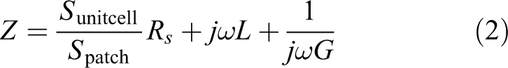
where, S unitcell and S patch are the area of the unit structure and the resistance patch. L and C represent the equivalent inductance and capacitance of the resistive patch. R s is the sheet impedance of the resistance patch.
The input impedance of the absorber can be expressed as:

Hence, one can get the reflection of the whole structure by:
To understand the intrinsic mechanism of the proposed structure, we monitored the surface current distribution of the cell structure at the peak resonant frequencies of 7.9 and 15.2 GHz. The surface current distribution in the conductive ink pattern layer and metal ground corresponding to the two absorption peaks is presented in Figure 4. As shown in Figure 4(a) and (b), at the frequency of 7.9 GHz, the surface current in the conductive ink layer was mainly concentrated on the outer edge of the circular ring resonator, while the current in the copper ground was in reverse with that in the conductive ink layer. The antiparallel current in the top and bottom layers led to the magnetic resonance. However, compared with that in the metal ground, the current density in the ink layer was much stronger, indicating that the electric resonances in the resistance layer were the main contributor to the EM wave absorption. As shown in Figure 4(c) and (d), there was no flow of the antiparallel current on the ground plate at the frequency of 15.2 GHz, so the magnetic resonance could be ignored while only the electric resonance contributed to the absorption.

Simulation results of the surface current distribution in (a) conductive ink layer at 7.9 GHz, (b) copper ground layer at 7.9 GHz, (c) conductive ink layer at 15.2 GHz, and (d) copper ground layer at 15.2 GHz.
The electric field distribution of the unit cell at the peak resonant frequencies of 7.9 and 15.2 GHz is presented in Figure 5(a) and (b), respectively. In both cases, the electric field was mainly concentrated at the edge of the ring resonator. Compared with the intensity of the electric field at the resonance frequency of 15.2 GHz, the intensity of the electric field at the frequency of 7.9 GHz was much stronger, which led to the higher absorptivity. The power loss distribution in the conductive ink layer at different absorption frequencies is illustrated in Figure 5(c) and (d). In Figure 5(c) and (d), it can be seen that the energy was strongly dissipated on the outer and inner edges of the ring resonator at the frequencies of 7.9 and 15.2 GHz, respectively. Hence, the upper and lower resonance frequencies were closely related to the outer and inner radius of the ink ring.
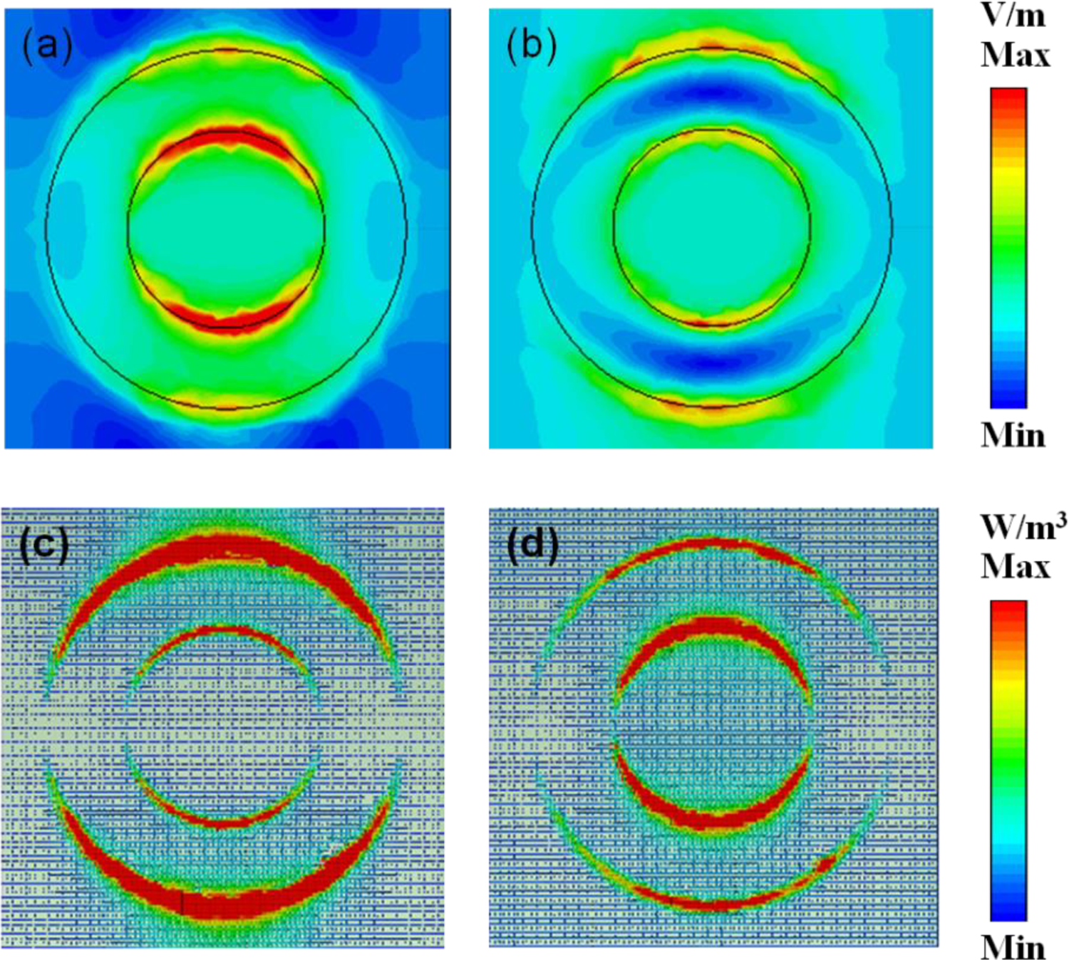
The distribution of electric field and power losses in the conductive ink layer at the peak absorption frequencies. (a) The electric field distribution in the conductive ink layer at 7.9 GHz. (b) The electric field distribution in the conductive ink layer at 15.2 GHz. (c) The power loss distribution in the conductive ink layer at 7.9 GHz. (d) The power loss distribution in the conductive ink layer at 15.2 GHz.
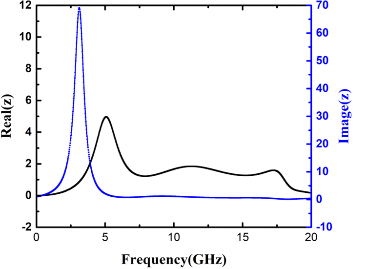
The normalized input impedance of the absorber is given by 32 :

To achieve the input impedance matching with the free space, Z(f) should be close to Z(f) = 1. The normalized input impedance of the proposed absorber is shown in Figure 6. In Figure 6, it can be seen that the input impedance was approximately matched with the free space impedance in the frequency range 6.58–16.38 GHz, providing a wideband absorption with a high absorptivity.
The normalized input impedance of the proposed absorber.
The effect of the material and structural parameters on the absorption spectrum was also analyzed. The influence of the loss tangent of the substrate on the absorption performance is presented in Figure 7(a). As shown in Figure 7(a), there was only a slight change in the absorptivity under different loss conditions, which meant that only a small amount of energy was consumed in the dielectric substrate. The influence of the substrate dielectric constant on the absorption spectrum is presented in Figure 7(b), where it can be noticed that with the increase in dielectric constant, the upper resonance frequency shifted to lower frequencies, indicating the absorption bandwidth of the proposed structure could be further widened by using the substrate with a smaller dielectric constant. The effect of substrate thicknesses on the absorption spectrum is shown in Figure 7(c), where it can be seen that with the increase in substrate thickness h, the effective capacitance between the upper and lower planes of the structure increased, leading to the redshift of the resonance frequencies. Further, the influence of surface resistance of the conductive ink on the absorption spectrum is presented in Figure 7(d), where it can be seen that with the increase in the surface resistance, the absorption bandwidth decreased rapidly. Hence, among all the parameters, the resistance of the conductive ink had a stronger influence on the absorption performance of the proposed absorber. Based on the analysis of absorption dependence on geometrical parameters, one can find an effective way to optimize the absorption spectrum of the proposed absorber. For instance, by decreasing the dielectric constant and thickness of the substrate, the absorption band at higher frequency will get an increase. Moreover, there is a trade-off of increasing the absorption band at lower frequency and enhancing total absorption rate by changing the radius of the resistive patch.

Absorption spectrum dependence on (a) loss tangent, (b) dielectric constant, (c) dielectric layer thickness, (d) surface resistance of the conductive ink, (e) outer ring radius, and (f) inner ring radius.
The effects of the outer and inner radii of the ink ring on the absorption spectrum are presented in Figure 7(e) and (f), respectively. As shown in Figure 7(e) and (f), as the outer ring radius increased, the first resonance peak shifted to lower frequencies, which indicated that the first absorption peak was determined by the outer radius R. Similarly, the absorption spectrum shown in Figure 7(f) indicates that the second absorption peak was closely related to the inner radius of the ring r, which confirmed our conclusions on power loss distributions mentioned above.
Absorption spectrum dependence on wave polarization and incidence angle
The polarization insensitivity of absorber is of great importance for its practical applications. To examine the absorber sensitivity to the incident polarization, we analyzed the wave polarization characteristics at different polarization angles. Simulation results for different wave polarizations are displayed in Figure 8. In this work, only polarization angles of up to 45° were studied because of the symmetry of the resonant structure. As illustrated in Figure 8, the absorption spectrum kept constant at different polarization angles; therefore, the proposed absorber was insensitive to the polarization of incident EM waves.
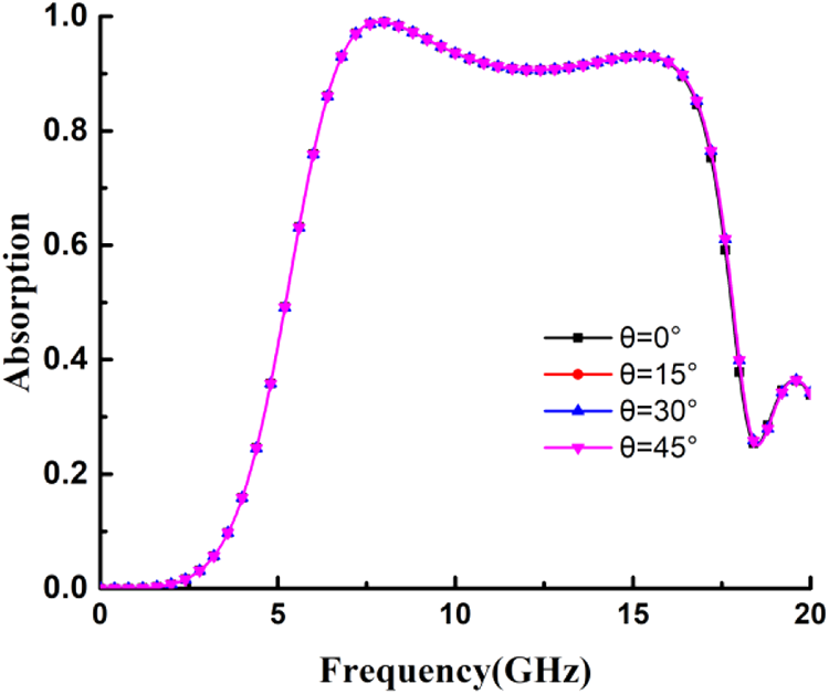
The absorption spectrum at different wave polarization angles.
We also studied the performance of the absorber at oblique incidence. The absorption spectrum of the transverse electric (TE)-polarized wave is shown in Figure 9(a). As presented in Figure 9(a), until the incident angle reached the value of 30°, there was almost no change in the absorption. However, as the incident angle continued to increase, the absorption decreased. Nevertheless, at the incident angle of 60°, the absorption was still above 0.7 in the frequency range 6.70–17.36 GHz, which proved the broadband absorption at large incident angles.

The absorption spectrum at different incident angles. (a) TE-polarized wave. (b) TM-polarized wave. TE: transverse electric; TM: transverse magnetic.
As shown in Figure 9(b), for the transverse magnetic (TM)-polarized wave, although there was a decrease in the absorption within a small bandwidth, the absorptivity was above 0.7 for incident angles of up to 60° in the frequency range 6.48–16.96 GHz. Hence, the proposed absorber achieved good broadband absorption performance for both TE- and TM-polarized waves.
Experimental verification
To demonstrate the performance of the proposed MA experimentally, a prototype of the proposed structure was fabricated, and it is shown in Figure 10(a). The conductive ink is made of carbon black, water, and a certain proportion of emulsion, while the resistance of conductive ink layer can be adjusted by changing its thickness. A sample of the overall size of 150 mm × 310 mm, corresponding to 13 × 27 unit cells, was fabricated using the screen printing technology. The ring areas filled with ink formed the FSS patches after cured by heating. The measurement setup is presented in Figure 10(b). We used two pairs of horn antennas, one for the X-band and another for the Ku-band, to measure the performance of the fabricated sample. The experiment was carried out in the anechoic chamber, using the horn antennas connected to a Rohde & Schwarz ZVA 40 vector network analyzer. In the measurement process, first, the reflection coefficient of the copper plate with the same size as the proposed absorber was measured and used as a reference value. Then, the fabricated sample was placed at the same location; the real reflection was calculated by subtracting the two measured reflected powers.

(a) Photograph of the fabricated sample. (b) The measurement setup.
The reflection coefficients of the absorber and the identical-in-size copper plate are presented in Figure 11(a). As shown in Figure 11(b), the measured absorption was in good agreement with the simulation results. In addition, a high absorptivity (greater than 0.9) was achieved in a wide frequency range (7–16.4 GHz).

The performance of the absorber at the normal incidence of TM wave. (a) Reflection coefficient S 11. (b) Absorption. TM: transverse magnetic.
Finally, we measured the absorption of the fabricated sample at different incident angles of the TM-polarized wave. In the measurement, we rotated both the transmitting and the receiving horn antennas from 0° and 45° on the azimuth plane and measured the reflection coefficient in 15° increment. As shown in Figure 12(a), the measured results show that the absorptivity was above 0.8 at the incident angles of up to 45°. Figure 12(b) shows the comparison of simulated and measured results at incident angles of 0° and 45°, while there is a good agreement between simulation and experiment. Hence, the proposed MA realized wideband absorption, achieving the polarization insensitivity and wide-incident-angle stability at the same time.

(a) The measured absorption spectrum of the absorber at the oblique incidence of the TM-polarized wave. (b) The comparison of simulated and measured results at incident angles of 0° and 45°. TM: transverse magnetic.
Conclusion
In this article, a wideband absorber based on conductive ink ring resonators with the polarization insensitivity and wide-incident-angle stability is presented. Using the proposed structure, the absorptivity of above 0.9 is achieved in the frequency range from 6.58 GHz to 16.38 GHz, realizing the relative absorption bandwidth of 85.4%. The absorption mechanism of the proposed structure is analyzed, and the effects of its structural parameters on the absorption spectrum are examined. In addition, the proposed design makes the absorber insensitive to the incident wave polarization, providing a high absorption for oblique incidences. The presented design is evaluated experimentally, and a good agreement between the simulated and measured absorption spectra is found in a wide frequency range. Thus, the proposed compact, low-cost structure has wide potential application in the field of microwave sensing, EM interference shielding, and stealth technology.
Footnotes
Declaration of conflicting interests
The author(s) declared no potential conflicts of interest with respect to the research, authorship, and/or publication of this article.
Funding
The author(s) disclosed receipt of the following financial support for the research, authorship, and/or publication of this article: This work was supported by the National Natural Science Foundation of China under project number 61871171.