
Abstract
Thanks to the ultrahigh flexibility of 2D materials and to their extreme sensitivity to applied strain, there is currently a strong interest in studying and understanding how their electronic properties can be modulated by applying a uniform or nonuniform strain. In this work, using density functional theory (DFT) calculations, we discuss how uniform biaxial strain affects the electronic properties, such as ionization potential, electron affinity, electronic gap, and work function, of different classes of 2D materials from X-enes to nitrides and transition metal dichalcogenides. The analysis of the states in terms of atomic orbitals allows to explain the observed trends and to highlight similarities and differences among the various materials. Moreover, the role of many-body effects on the predicted electronic properties is discussed in one of the studied systems. We show that the trends with strain, calculated at the GW level of approximation, are qualitatively similar to the DFT ones solely when there is no change in the character of the valence and conduction states near the gap.
Keywords
Introduction
Much of the emphases on 2D materials
1
–3
was born with the discovery of graphene, for which the Nobel Prize in physics was awarded to Novoselov and Geim in 2010.
4
Graphene is a 2D crystal made up of carbon atoms arranged in a hexagonal honeycomb form; it is one million times thinner than paper, almost transparent, and, at the same time, is the strongest material in the world.
5,6
Its electronic structure can be easily derived from a simple tight-binding model, which explains the presence of bands with conical dispersion intersecting at the Fermi level, thus making graphene a semimetal.
7
Massless Dirac fermions move in graphene as fast as
Following the route of graphene, broad families of 2D materials are hence continuously developed and studied in view of their interesting physical properties and of a large number of their envisaged device-oriented applications. 9,10 Because of their atomic-scale thickness, they are characterized by weak dielectric screening, strong light–matter interaction, and highly bound excitons. Moreover, atomic and molecular doping, 11 –13 external fields, 14 and also strain 15 –17 may have a very deep impact on their electronic and optical properties. In particular, strain engineering is very exciting since, differently from 3-D traditional materials, 2D materials can endure remarkably large mechanical strain (up to 10%), hence creating opportunities to modulate their physical properties for interesting device applications.
Silicene, 18 –20 the silicon-based counterpart of graphene, represents the first exciting material merging the exceptional physical properties of graphene with the simplicity of easily integrating it in already existing and largely developed silicon-based technology. 21,20 A field-effect transistor has been reported at room temperature. 22 Further interest in silicene arises from its predicted nontrivial topological properties. 23 Freestanding ideal silicene presents a buckled honeycomb structure. 19 Like graphene, silicene has a semimetallic behavior and possesses (in the absence of spin–orbit corrections) massless fermions at the k-point of the brillouin zone (BZ). 24,25
Other members of the so-called X-enes family (borophene, germanene, stanene, phosphorene, arsenene, antimonene, bismuthene, and tellurene) are also of particular interest for their excellent physical, chemical, electronic, and optical properties. 26
The evidence that bulk group-III nitrides are among the most important materials for solid-state lighting, as witnessed by the Nobel prize awarded in 2014 to Akasaki, Amano, and Nakamura, stimulated in the last years several theoretical 27,28 and experimental 29 –31 studies on 2D honeycomb III-N sheets. From the experimental side, their growth is very challenging because, similar to the case of silicene, no simple route to mechanical or chemical exfoliation can be used, due to their 3-D wurtzite structures (only BN crystallizes in the hexagonal layered form in bulk). However, several promising experimental attempts to realize 2D III-nitrides have been reported so far.
Among layered materials, for which exfoliation is possible, transition metal dichalcogenide (TMD) occupies a prominent place in recent worldwide research.
32
–35
They are of type MX
2, where one layer of transition metal atoms (M) is sandwiched between two layers of chalcogen (X) atoms, crystallizing mainly in the hexagonal or rhombohedral forms with metal atoms having octahedral or trigonal prismatic coordination. Among this broad family, group-VI TMD (
In this article, we use first-principle DFT calculations to study the role of biaxial uniform strain on the structural and electronic properties of 2D materials beyond graphene: silicene, group III-nitrides, and TMD. In particular, we focus on the behavior of their band structure, electronic gap, workfunction (WF), ionization potential (IP), and electron affinity (EA) and perform a comparative analysis for nonpolar (graphene and silicene), polar (aluminum nitride (AlN) and gallium nitride (GaN)) honeycomb lattices, and TMD (molybdenum disulfide (MoS2) and molybdenum ditelluride (MoTe2)) in the monolayer and bilayer form.
Methods and computational details
All the DFT calculations to obtain the structural and electronic properties have been performed using the Quantum-Espresso code 42 within the local density approximation (LDA), 43 perdew becke ernzerhrof (PBE), 44 XC functional for nitrides (TMD). For the case of the two X-enes (graphene and silicene), we performed calculations using both LDA and PBE with the specific goal to look at the effect of local or semilocal XC on the calculated values of the work functions. The van der waals (vdW) correction 45 has been applied to take into account the interaction between the layers in TMD BL.
For X-enes and nitrides (TMD), we used scalar (fully)-relativistic optimized norm-conserving 46 pseudopotentials from the quantum-espresso (QE) repository.
The self-consistent density for graphene and silicene was computed using a 15 × 15 × 1 k-point sampling for the ground state with plane wave cutoff of 100 Ry. For nitrides, we used a nonshifted 18 × 18 × 1 k-point sampling for the ground state and a plane wave cutoff of 100 (200) Ry for the structural optimization and band structure of AlN (GaN). For TMD, we sampled the BZ using a uniform 18 × 18 × 1 mesh and used a plane wave cutoff of 120 Ry.
To simulate isolated layers, vacuum sizes of 15 and 20 Å have been chosen for X-enes and nitrides, respectively, while 17.8 (16.5) Å has been used for TMD-ML (BL). The geometry of each system has been relaxed at each value of strain until the forces on the atoms were less than
Equilibrium lattice constant a 0, buckling for X-enes and nitrides, and X-M-X angle for TMD.

d 1: the vertical distance chalcogen–chalcogen; d 2: vertical distance between layers; TMD: transition metal dichalcogenide; GaN: gallium nitride; AlN: aluminum nitride; MoTe2: molybdenum ditelluride; MoS2: molybdenum disulfide.
To assess the role of many-body effects, for one of the studied systems, that is, the MoTe2 monolayer, we went beyond the single-particle approach. On top of the DFT simulations, we performed one-shot perturbative
Results
The main goal of this work is to describe how the electronic properties of different classes of metallic and semiconducting 2D materials can be tuned via the application of a uniform biaxial strain with the aim to highlight similarities and differences among the different systems.
For all the 2D materials, we have calculated the WF obtained as the energy difference between the Fermi energy EF
and the vacuum potential
Graphene and silicene
For these two X-enes, we observe that for increasing compressive strain, the WF decreases, whereas it increases for increasing tensile strain (see Figure 1). For graphene, this behavior is in substantial agreement with the existing literature 54,55 and it has been explained in terms of a strain-induced enhancement of the density of states (DOS) close to the Fermi level. 56,57 Results for silicene are qualitatively similar to the ones obtained for graphene. In the tensile region, the WF variation due to a 10% of strain is found to be 0.15 eV, in good agreement with the results of Qin et al., 58,59 where a change of about 0.2 eV has been obtained.

Dependence of the WF by the strain value using PBE and LDA XC potentials. Top panel: results for graphene. Bottom panel: results for silicene.
We observe that, for both the systems, a simple argument of plausibility of this behavior is based on the fact that as long as the materials are stretched, the interaction among the ions of the lattice decreases, thus approaching the behavior of isolated atoms in the limit of infinite tensile deformation. The ionization potentials for C and Si atoms are 11.2 and 8.1 eV, respectively, and these values are much higher than the WF of their correspondent 2D forms at equilibrium, 4.24 eV for graphene, and 4.35 eV for silicene. For this reason, it is expected that the WF of these materials, characterized by fully covalent bonds, should grow with increasing uniform tensile deformation.
To test the possible dependence of our results on the choice of the XC potential used to describe the various systems, we have analyzed the strain dependence of the WF of graphene and silicene both within the LDA and PBE scheme for the XC term. The results of this analysis are shown in Figure 1 in different colors. It is noted that the choice of the functional affects the value of the WF by adding a constant shift of 0.24 eV for graphene and of 0.41 eV for silicene. In particular, the zero strain WF for graphene ranges from 4.24 eV in PBE to 4.48 eV in LDA, thus producing a spread of results, which is fully consistent with values in the range from 4.28 eV to 4.5 eV found in the literature. 54,55,60 –62 But, interestingly, we observe that the functional induced variation turns out to be a constant shift, which is independent of the strain value. Thus, we can conclude that the strain-induced variations of the WF do not depend on the choice of functional and can be assessed unambiguously within the DFT framework.
Nitrides monolayers: AlN and GaN
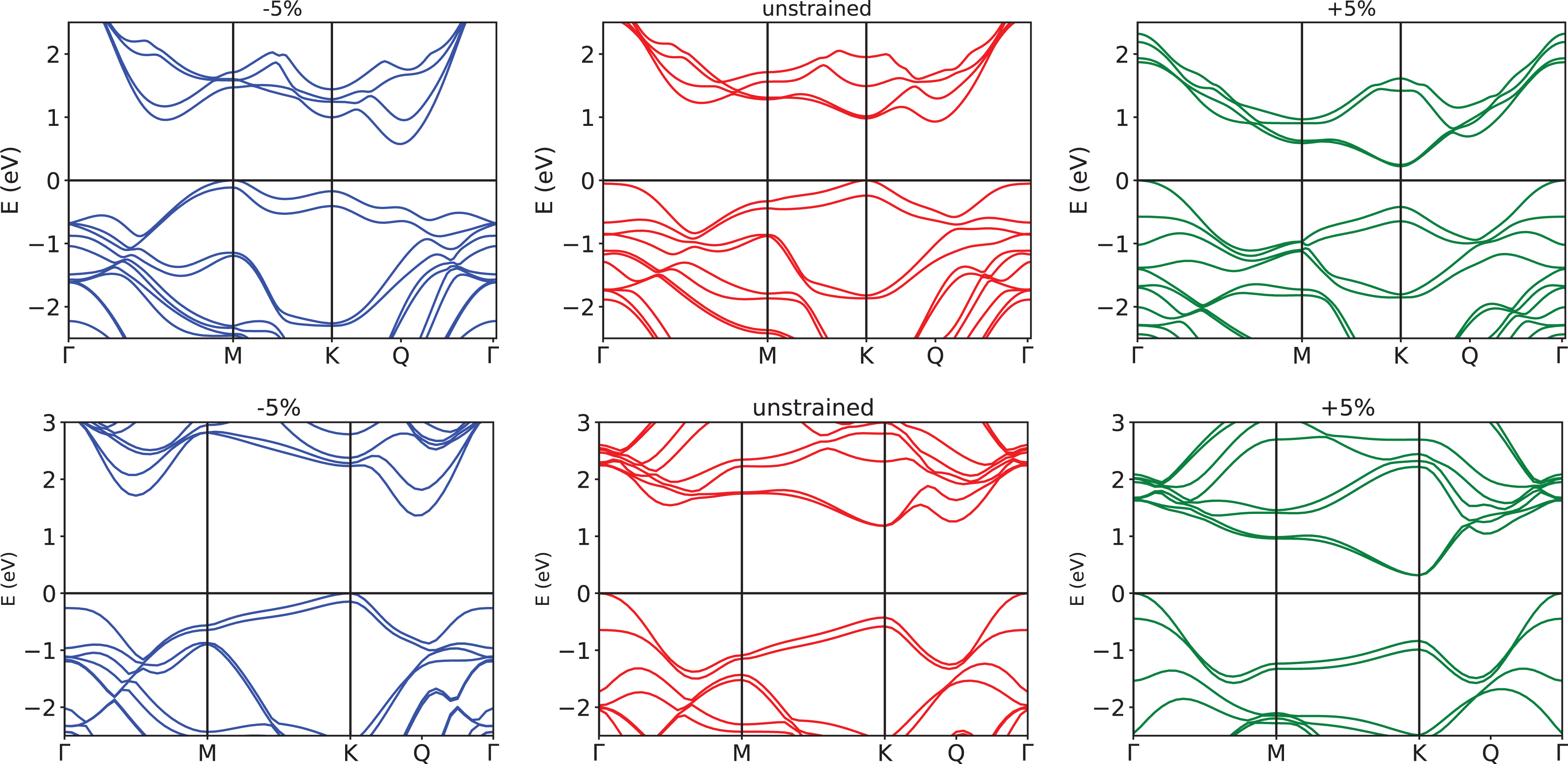
The 2D nitrides have the same flat honeycomb structure as graphene but with polar bonds due to the different electronegativity of the lattice atoms. To understand the trends of the IP, WF, and EA under strain, it is important to analyze their band structures. These are shown in Figure 2 for GaN and AlN at 0, −4%, and 4% uniform strain. In agreement with existing literature,
27
we have found that at zero strain, both AlN and GaN have an indirect bandgap

Band structrure of AlN (top) and GaN (bottom) monolayers for biaxial uniform strain of −4% (blue), 0% (red), and 4% (green). The dashed gray line indicates the VBM for the unstrained material, set as zero energy.
While AlN remains an indirect gap material for all the values of considered strain, GaN undergoes an indirect to direct gap transition at the compressive strain of about −4%. It is worth to mention that unstrained GaN has an indirect gap only at the DFT level, which switches to direct when the GW corrections are introduced.
27,63
In the case of strain, the VBM switches from K to Γ, because the state at Γ goes up in energy under compressive strain, while the corresponding eigenvalue at K does not show a big variation. This behavior can be explained by analyzing the character of the KS wavefunction at Kv
and at

Plot of
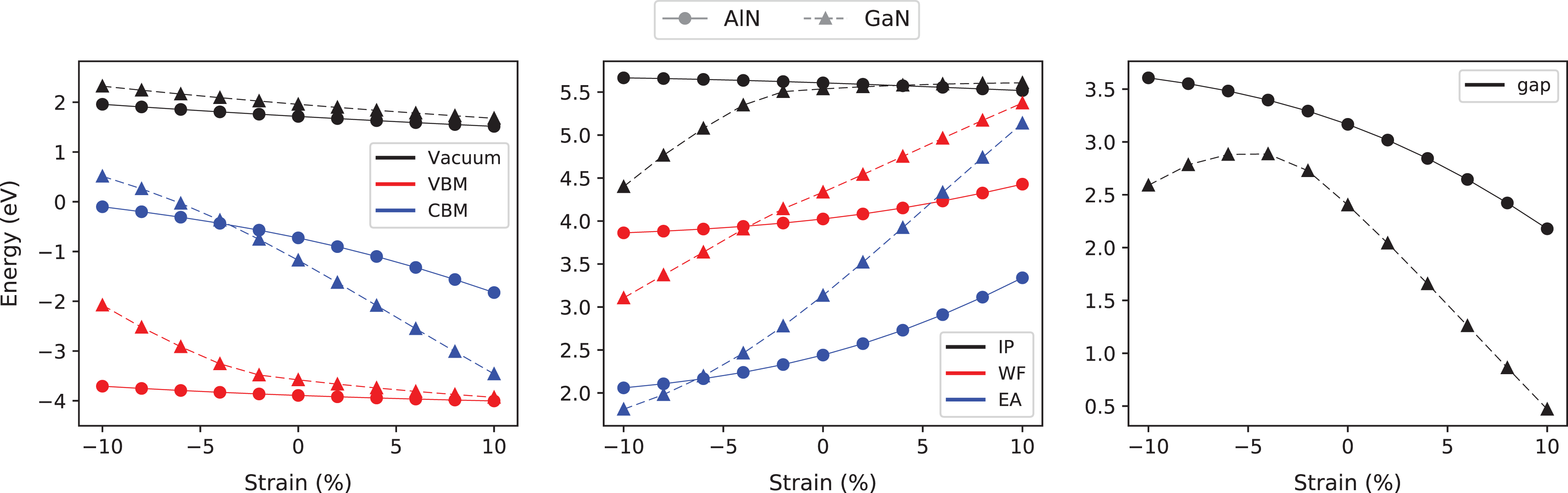
AlN (solid lines) and GaN (dashed lines). Left panel: vacuum level (black), CBM (blue), and VBM (red) dependence on the strain. Center panel: IP (black), EA (blue), and WF (red) dependence on the strain. Right panel: gap dependence on the strain.
It is worth to notice that the corresponding IP of AlN shows an opposite trend, increasing (decreasing) when the compressive (tensile) strain increases. This can be explained, again, in terms of the stronger localization of the electronic charge near the nitrogen atoms that occurs in AlN, with respect to the case of GaN, due to the larger difference in the electronegativity between anion and cation. The EA is given by the position of the conduction bands bottom, and both materials show a similar behavior: EA increases (decreases) for increasing tensile (compressive) strain. The CBM is always at Γ and from the analysis of the KS wave functions, it is due to a hybrid of s states of the cation (Al/Ga) and anion (N), where the former gives a larger contribution. Also, for GaN, a small contribution from the d states appears. This analysis explains why the slope of CBM and then of EA is steeper in GaN with respect to AlN. The dependence of WF and gaps from strain is then a direct consequence of the IP and EA behavior.
TMD: MoTe2 and MoS2
Upon the application of strain, the electronic properties of TMD show a more complicate behavior with respect to those of X-enes and nitrides. Moreover, despite the similarity in their atomic structures, the electronic properties of MoS2 and MoTe2 monolayers and bilayers have similar but not completely equivalent trends. 64,65
MoTe2 and MoS2 monolayer
In agreement with the existing literature, the two

Electronic band structure of monolayer MoTe2 (top) and MoS2 (bottom): under compressive strain (left/blue), under tensile strain (right/green), and with zero strain (center/red).

Orbital projected band structure of MoTe2 ML: p-orbitals of Te (top panel) and d-orbitals of Mo (bottom panel).
The analysis of Qc
shows a similar composition of Kv
with minor contribution from

Plot of
Interestingly, the behavior of MoS2 and MoTe2 under uniform compressive strain is very different. In MoS2-ML, the CBM moves from K to Q for strain above

Dependence on the strain of vacuum level (black), CBM (blue), VBM (red) (left panel); IP (black), EA (blue), WF (red) (central panel); and (c) electronic gap (right panel) for monolayer MoS2 (solid lines) and MoTe2 (dashed lines).
For what concerns tensile strain, we see that the IP of MoS2 decreases by increasing tensile strain. This can be explained in the following way: from very small strain values (less than 1%), the VBM moves from Kv
to
For both TMD-ML, EA decreases when reducing the lattice parameter up to the crossover of the CBM from Kc to Qc . Then, EA begins to increase with a very small rate when Qc becomes the global conduction band minimum (central panel of Figure 8).
From the analysis of the data shown in the central panel of Figure 8, and similar to the case of nitrides, it is clear that the behavior of the WF depends on both IP and EA curves and shows an intermediate behavior. We can say that the WF and EA values for the two TMD-ML have a qualitatively similar behavior: an increase with a change in the slope that occurs when the direct to indirect bandgap crossover happens for low compressive strain. The linearity of EA is due to the smoothness of the vacuum potential and CBM (left panel), while the WF values are affected by the more complex behavior of the VBM (left panel) with strain. Finally, the bandgaps (Figure 8, right panel) have a totally different trend for MoS2-ML and MoTe2-ML, showing a much more symmetrical behavior of MoTe2 for tensile and compressive strain.
Beyond the monolayer
TMD bilayers and multilayers are known to be indirect bandgap semiconductors. MoS2 (MoTe2) shows an indirect gap
Band structure of bilayer MoTe2 (top) and MoS2 (bottom): under compressive strain (left/blue), under tensile strain (right/green), and with zero strain (center/red).
The p X-orbital composition at Qc
and
In this regard, it is worth to mention that for MoTe2 bulk, we specifically tested how our simulated structural parameters (a = 3.54 Å, Mo–Mo vertical distance between two different layers 7.33 Å) are obtained using the selected vdW functional, reproduce the experimental data (a = 3.54 Å, Mo–Mo distance between two different layers 7.33 Å) reported by Knop and MacDonald, 70 finding a very good agreement.
Moreover, always for MoTe2-BL, we also tested other two vdW functionals taken from the study by Grimme 71 and Barone et al., 72 respectively. In both cases, the final optimized structures are very similar to the one reported in Table 1, with lattice parameter a and Te–Te intralayer vertical distance, which changes less than 0.3%. Only using the second functional, we observe a reduction of 2.6% of the interlayer vertical distance. The electronic band structure does not show relevant changes near the gap region with the largest downshift of the VBM at Γ of 0.05 eV.
In Figure 7, we show the charge density plot of the Qc
state for MoS2 (left) and MoTe2 (right) bilayers, where the important contribution coming from p-orbitals of chalcogen atoms is evident. Similar to what discussed above, the very delocalized nature of these orbitals for the case of Te is evident from the figure. MoS2 and MoTe2 bilayers show, already at zero strain, different values of VBM and CBM due to the different hopping between p of the two adjacent layers, as shown in Figure 7. When tensile strain is applied in both BL, Kc
and Kv
go down in energy in agreement with the monolayer behavior (right panels of Figure 9). For compressive strain, similar to the monolayers, Qc
goes down in energy and, for MoTe2, Mv
becomes the VBM when
In other words, trends previously discussed for monolayers remain qualitative similar for bilayers (see Figure 9), but different values of strain are needed to obtain changes in VBM and CBM with respect to the MLs. Moreover, MoTe2-BL results are more sensitive to strain with respect to MoS2-BL. This is also highlighted in Figure10, where the IP curves of the monolayer and bilayer of MoS2 and MoTe2 are reported, respectively, in the top and bottom panels.

IP versus strain for monolayer (red) and bilayer (blue) of MoS2 (top panel) and MoTe2 (bottom panel).
Role of many-body effects
Despite the DFT electronic properties of 2D materials that are affected by the well-known bandgap problem, previous works have suggested that their behavior under strain reproduces, at least qualitatively, the one obtained with more refined excited state methods, such as
Because of the heaviness of GW calculations, we have limited our analysis to zero strain and to one value of compressive (

Comparison of GW (solid) and DFT (dashed) energy of CBM (red) and VBM (blue). Values for the local minimum of the conduction band at K (green) are also reported.
Conclusions
We have presented a systematic study of the effect of uniform biaxial compressive and tensile strain on the electronic properties of several 2D materials ranging from semimetallic ones, like the X-enes, to semiconductors like nitrides and TMD.
Each material shows its own behavior strictly linked to the changes in the band structures and to the orbital character of the CBM and VBM. In all monolayers, the WF always increases with the lattice parameter, while the IP and EA show material-dependent trends.
The slope of the IP versus strain is usually positive, but exceptions arise for AlN (very small negative slope) and MoS2 (where the right and left derivatives are different). The bilayers appear to be much more sensitive to strain than the isolated layers, hence, the curves are similar only in some regions. The difference in behaviors for nitrides and TMD is explained in terms of the localization of the VBM and CBM wave functions. We have also shown that the choice of the XC potential while affecting the absolute value of the WF does not change the general behavior of the electronic properties with respect to the strain. Finally, we have demonstrated that special care has to be used when the character of the VBM or CBM changes with the strain, as the DFT and
Footnotes
Acknowledgements
We thank Dr M Stella Prete for providing us the atomic structures of unstrained nitride monolayers. We acknowledge ISCRA–B and C initiatives for awarding access to computing resources on Marconi at CINECA HPC center.
Declaration of conflicting interests
The author(s) declared no potential conflicts of interest with respect to the research, authorship, and/or publication of this article.
Funding
The author(s) disclosed receipt of the following financial support for the research, authorship, and/or publication of this article: MP and OP acknowledge INFN for financial support through the National project Nemesys. EU funding through the MSCA RISE project DiSeTCom (GA 823728) is gratefully acknowledged.