
Abstract
Ways to achieve highly efficient electromagnetic absorption over a broad bandwidth and broad angular spectrum have been discussed extensively in the past decades for various applications, such as low reflection devices and energy harvesting. To satisfy the efficiency requirements, metamaterial approaches have been explored in recent years. In this context, most studies have suggested the use of frequency selective surfaces or arrays of plasmonic resonators, which limit bandwidth and angular spectrum of performance. Here, we explore the application of refractory Brewster metasurfaces for photovoltaic applications. By matching the surface impedance of metasurfaces and free space at the Brewster angle, we show that metasurfaces can lead to efficient light absorption, and their response can be controlled accurately both in the angular and in the frequency spectrum to match the requirements of energy harvesting systems and facilitate large efficiency, high-temperature energy harvesting.
Introduction
Metamaterials have provided a viable solution to a variety of practical challenges in modern technology. 1 –16 In parallel, anomalous reflection and transmission in metasurfaces have inspired several exciting opportunities in various fields of research, from radiofrequencies to optics. 17 –24 As an important application of metamaterials and metasurfaces, electromagnetic energy absorption with high efficiency has been actively studied in many forms and shapes. However, some limitations exist in their response, mostly in their typically narrow absorption bandwidth and angular spectrum. So far, studies of metamaterial absorbers have focused on resonance-based absorption, 25 –31 which leads to small footprints but at the cost of performance degradation. For example, in Landy et al.’s 25 study, the proposed metasurface supports an Resistor-Inductor-Capacitor (RLC) resonance that provides perfect absorption at the desired frequency. An analogous approach was developed for photonics, which is applicable to energy harvesting and other photonic applications, 32 –35 also hindered from the same limitations of narrowband absorption with a notch-shaped response. These responses may be useful for scenarios involving sensing but are not necessarily appealing for broad-spectrum energy harvesting. Deviating from the resonance-based approach, gradient metasurfaces have been explored for broadband applications. By steering waves into extended paths inside an absorptive layer, the metasurface can trap the impinging energy efficiently into a thin layer of photovoltaic material. 36 This approach also has limitations in terms of angular spectrum response, since the application design typically assumes normal incidence. Here, we explore absorbing metasurfaces based on the Brewster effect, which offer high efficiency of absorption both over a broad bandwidth and in the angular spectrum. Brewster phenomena occur when the transverse free-space impedance at the angle θ B matches the metasurface impedance Z s. To design metasurfaces that operate in this regime and optimize their frequency and angular response, we consider slit metastructures inspired by previous related works. 37 –41
As shown in Figure 1(a), the metasurface is characterized by three geometrical parameters, the periodicity d, slit width w, and vertical thickness t. A tapering in the slits can be added to improve impedance matching and increase the absorption path, with the taper length shown as l. When the impinging light hits the metasurface at θ B, the wave tunnels through the slits as a result of impedance matching, launching surface plasmon polariton propagation if the structure is composed of plasmonic–dielectric interface. The slit width and periodicity determine the complex value of the guided vector, directly related to the Brewster angle θ B.
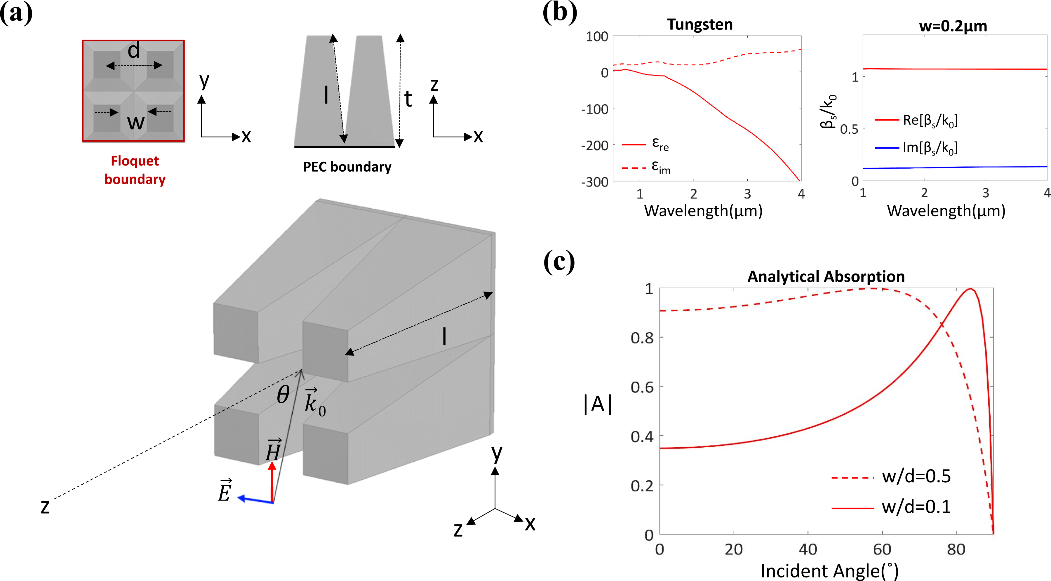
(a) Metasurface geometry, with the red edge of periodic boundaries and black edge of PEC boundary condition. The 3-D figure shows a TM wave incident toward the structure. (b) Left panel: permittivity dispersion of tungsten. Tungsten has a positive real part of permittivity under λ = 0.9 μm, while it has a metallic response at larger wavelengths. Right panel: dispersion of the guided wave number with frequency above plasmonic frequency. (c) Calculated absorption. Depending on the ratio of period and slit width, the angular response of absorption is varied. Broad angular absorption is achieved with a moderately large ratio, while narrow angular absorption around grazing angle is achieved with a small ratio. TM: transverse–magnetic; PEC: perfect electrical conductor.
The material composition of the metasurface is another important degree of freedom. Plasmonic materials, such as copper and gold, support SPP propagation at the interface with a dielectric material which can guide the energy adiabatically toward the bottom of the metasurface along the tapering paths. Therefore, metasurfaces composed of plasmonic–dielectrics interfaces can enhance energy harvesting with large efficiency, offering practical benefits for these applications. However, common plasmonic materials suffer from a low melting temperature, making them impractical for thermophotovoltaic applications. For this reason, here we focus on tungsten as a refractory material instead of gold. 37 –41 In the following section, we outline the theory and properties of Brewster metasurfaces composed of tungsten and show how we can engineer the features of absorption with its bandwidth, angular spectrum, and width of angular absorption within a relatively simple design space. Later on, we compare their response to dielectric Brewster metasurfaces and draw our conclusions.
Theory and results
Tungsten is a refractory material that can withstand high temperatures without major degradation, and it has both metallic and dielectric response in the optical spectrum, as shown in the permittivity dispersion in Figure 1(b). In this study, we consider free space for the filling between tungsten slits. Considering a one-dimensional periodic structure, Z
s can be defined as

Since β s is nearly linear with k 0 over a broad range of frequencies, θ B strongly depends on the ratio “w/d” rather than frequency in equation (1). In Figure 1(c), the absorption has been calculated analytically based on this formulation and shows how the ratio w/d affects θ B. The solid line shows the case for w/d = 0.1, offering large absorption at steep, grazing angles, around 90° but low absorption around normal incidence. This response is not desirable for most energy harvesting applications, for which broad angular spectrum, including the normal direction, is ideal. High absorption over a wide angular spectrum can be achieved tuning the Brewster angle to around 60°, as shown by the dashed line in Figure 1(c), for w/d = 0.5 supporting θ B = 57°. This example supports absorption above 0.9 from 0° to 70°. In frequency spectrum, this property holds over broad bandwidths since the ratio between βs and k 0 is constant, as it is confirmed in Figure 1(b).
The dual operation corresponds to transverse electric (TE) excitation. In this case, no Brewster effect is possible, since the plane wave cannot easily couple to the slits, but we can expect high absorption around normal incidence when the TM response is not too selective with the angle of incidence. While the angular spectrum of absorption is tunable simply controlling the ratio of width and period, the boundaries of the available bandwidth where absorption takes place are interestingly determined in simple terms by two geometrical parameters: the thickness of the structure for the upper cutoff wavelength and the period of the grating for the lower cutoff wavelength. The dispersion of the guided vector βs also has a predictable role. Interest in determining the maximum bandwidth of absorption for a given absorber thickness has been a long-standing problem, 42 –45 which has culminated in the derivation of Rozanov’s bound, 46 yielding a fundamental limit between maximum bandwidth of absorption and thickness of the structure. Following Rozanov’s bound, the absorption window only depends on the static permeability μs of the involved material, here equal to the one of free space, the overall thickness of the absorber, and the acceptable residual reflectivity of the absorber ρ0. For the geometry of interest, therefore, the available bandwidth absorption is defined as

where λmax and λmin are the upper and lower cutoff wavelength. Assuming ρ0 = 0.3, for t = 3 μm, we obtain a maximum wavelength bandwidth of about 39 μm and 13 μm for t = 1 μm. In the study, achievable bandwidths fall close to the Rozanov’s bound in several of our designs, with the discrepancies typically associated with nonoptimal tapering of the slits, and the residual dispersion of the SPP modes responsible for absorption.
To corroborate the aforementioned analysis, finite-difference time-domain (FDTD) simulations have been performed for the structure in Figure 1(a). We chose a filling width w of 25 nm, supporting

The absorption efficiency over broadband frequency range from near infrared range to infrared range. All figures are the results simulated with FDTD simulations. Structures are designed with the same slit width “w = 25 nm” and with different periodicity (a) d = 35 nm, (b) d = 75 nm, and (c) d = 150 nm. Analytically calculated Brewster angle are (a) θ B = 0°, (b) θ B = 50–55°, and (c) θ B = 70–75°, and the Brewster angles of the numerical results match with the calculation results as shown with white dashed line. FDTD: finite-difference time-domain.
Next, structures with different vertical thicknesses were studied numerically to explore how they affect the absorption within the bandwidth of interest. The thickness is sampled between t = 300 nm and t = 600 nm, and the Brewster angle θB is fixed to 50–55° with a periodicity d = 75 nm and slit width w = 25 nm. The solid lines in Figure 3(a) show the absorption when the metasurface has t = 300 nm and 600 nm. As we discussed before, the thickness controls the upper cutoff wavelength of the absorption bandwidth, and it is confirmed by the results. With the same material and dimensions, broadband absorption is achieved up to λ = 2.5 μm for t = 600 nm, but with t = 300 nm, it stops at λ = 1.8 μm. To clarify the relation between thickness and bandwidth, we also simulated the geometry with no-tapered slits when t = 600 nm, with same dimensions, and the results are given with dashed lines. For the same thickness, the result shows that tapered structures support a higher cutoff wavelength, offering longer propagation lengths and less reflections due to adiabatic focusing at the end of the slits. Ripples of high absorption in the frequency spectrum correspond to Fabry–Perot and Fano resonances that occur because of transverse and/or longitudinal resonances in the structure, associated with the finite dimensions of the tapering length and induces Fabry–Perot resonances in the longitudinal direction and transverse resonances stemming from the grating periodicity.

(a) Absorption of the structure with d = 75 nm, w = 25 nm with different thickness of t. With the same amount of guided vector β s, the structure with t = 600 nm gives the larger waveband of absorption stretched to 2.5 μm (red solid line), while the structure with t = 300 nm gives waveband stops at 1.8 μm. Non-sloped structure of the same dimension is simulated to compare the results of sloped structure (dashed line). Comparing the results with the same thickness t = 600 nm, the slope of the structure supports the longer waveband and the higher efficiency of absorption with its geometry. (b) and (c) The result of total angular absorption from θ = 0° to θ = 89.9°. Both the non-sloped and the sloped structure supports broad angular absorption, but the waveband is cut clean with the non-sloped structure, while there is some residue of absorption with the sloped structure.
Rozanov’s bound for ρ0 = 0.1 yields a maximum absorption bandwidth of 2.1 μm and 4.2 μm as t = 300 nm and 600 nm at normal incidence. Both structures support an absorption window within Rozanov’s bound. Figure 3(b) and (c) show the angular and frequency response for the non-tapered and tapered geometries, where all other dimensions are the same with t = 600 nm. It is worth noting that the non-tapered structure supports an interesting sharp cutoff wavelength in broad angular spectrum for the absorption window, which stops at λ = 1.6 μm, while the tapered structure shows a more gradual absorption decline after λ = 2.5 μm. The response of the non-tapered structure is quite interesting for energy harvesting applications in which the absorption spectrum of interest is confined at shorter wavelengths. To avoid temperature increase where the absorbed energy is not efficiently converted to electrical energy, it is desirable to avoid absorption at longer wavelengths, and the response in Figure 3(c) is ideal for this purpose. Similar sharp cutoffs and thermal engineering responses may be ideal for radiative cooling applications, and this geometry appears well suited also in these scenarios. 47 –50
So far, we discussed how the geometrical parameters of the metasurface affect the absorption using one material, tungsten. Next, we consider the case of bulk Si, as an alternative material that supports dielectric property overall the optical spectrum. The geometrical parameters that we consider are: w = 25 nm, d = 75 nm, and t = 300 nm, and we compare the performance of the two metasurfaces from λ = 0.2 to λ = 2 μm in Figure 4. For the tungsten structure, the guided vector can be calculated as

Simulated results of the metasurface with tungsten and silicon. (a) The tungsten structure provides high absorption for all frequencies and angles in the considered range. (b) The silicon metasurface supports high absorption until λ =0.5 μm supported by lossy dispersion relation, and only sharp resonances contribute to absorption for the wavelengths above λ = 0.5 μm.
Conclusion
To conclude, we discussed here the design and implementation of Brewster metasurfaces for energy harvesting applications, supporting broadband and omnidirectional absorption, which can be controlled by changing its geometrical parameters and the materials involved. Compared to previous approaches, the Brewster metasurface supports large absorption over a broad and controllable range of angles and frequencies, tweaking simple geometrical parameters, enabling an easy design. Interestingly, we found that the tapering angle of the slits can be used to control and sharpen the cutoff wavelength of absorption, which may be useful for thermal management. We applied these concepts for energy harvesting applications at infrared and visible frequencies, but the same concept is scalable and applicable to the radiofrequency spectrum following a similar analysis and design procedure.
Footnotes
Acknowledgments
We acknowledge useful discussion with Dr Julius Yellowhair and Dr Shubash Shinde.
Declaration of conflicting interests
The author(s) declared no potential conflicts of interest with respect to the research, authorship, and/or publication of this article.
Funding
The author(s) disclosed receipt of following financial support for the research, authorship, and/or publication of this article: This work was partially supported by Sandia National Laboratory and by the Welch Foundation with grant no. F-1802.