
Abstract
Evolution of deformation and stress in growing thin films has been studied in this work using computational simulations that resolve matter at atomic length and time scales. For the surface layers of films laying on the substrate of a dissimilar material, the stress distribution analysis around defects becomes more challenging. Herein, spatial and temporal distribution of deformation and associated stress evolution are presented for different thin film formation events including (1) sub-monolayer growth during an early film nucleation stage and (2) coalescence of adjacent monolayer “islands.” Validity of the stress computed via local computations of the virial expression for stress in a system of interacting particles was checked by comparing to results obtained from considerations of local atomic deformation in conjunction with existing expressions for epitaxial thin film growth stress. For the geometries studied here, where a monolayer of film with a highly characterized linear defect, as in the case of a stacking fault, was simulated for coalescence, fairly good agreement was found. This result demonstrates that, for similar defects at the surface layer, with sufficient sub-ensemble averaging of the standard virial expression for stress, semiquantitative spatial stress distribution information can be obtained from atomic scale simulations. Using our validated stress computation method, we reveal significant stress localization during thin film growth processes, leading to pronounced differences in maximum and minimum stress observed over very small spatial extent (of order multiple GPa over 3–6 nm distances). One prominent mechanism of stress localization revealed here is coalescence between adjacent growing islands. For geometries explored here, stress manifesting during coalescence is highly localized.
Keywords
Introduction
Advances in technology have made fabrication of devices with nanometer scale dimensions possible; a subclass of such devices are those fabricated on substrate surfaces with micro/nanoscale features and/or surface modifications. Deployment of these novel devices in optoelectronics, piezoelectric and photovoltaic technologies, magnetic storage devices, and conductor/semiconductor applications has been reported to provide better performance with lower material cost. 1 Thin films, particularly metallic thin films, are one of the most common products in this field; they are either used as a coating material or as a sheet from which smaller parts are manufactured. 2 One method of growing thin films is via atomic deposition of the film material in vapor phase onto a substrate. Intrinsic stress, which evolves during the growth of the film or after completion of the deposition process, has a significant effect on the film performance and reliability due to the inherently small dimensions which can result in film failures, that is, buckling, delamination, or peeling. 2,3
Film growth typically occurs in one of a few observed modes, distinguished by the morphology exhibited by the growing film. In one such mode, Volmer–Weber growth, three stages have been identified: an initial stage during which discrete islands nucleate at random locations on the surface, an intermediate stage when growing islands begin to impinge on one another and coalesce into a continuous film, and a late stage when the continuous film thickens. A related growth mode is Stranski–Krastanov where an initial wetting layer of the film material forms on the substrate, followed by nucleation of discrete islands on the wetting layer. Consistent layer-by-layer growth is Frank van der Merwe mode.
Stress evolution during different stages of the film growth process has been studied experimentally and different mechanisms are proposed to be contributing to observed stress evolution. For VW growth, in the initial nucleation stage, compressive stress has been proposed to be due to Laplace pressure effects, 4 –6 misfit stress, 2,5,7 –9 or effective force dipoles generated by adatom motion on the surface. 10,11 In the next stage, tensile stress arises when growing islands start to coalesce with each other, forming grain boundaries. The elimination of surface energy due to island coalescence comes at the expense of some elastic energy manifesting. Tensile stress generation mechanisms for different system configurations have been demonstrated via different models 6,11 –17 for the coalescence stage. When coalescence events are mostly completed, the film thickens as more atoms are deposited. During this final stage, for high mobility materials, tensile stress is reported to relax and/or more compressive stress is generated. The cause of this remains a matter of debate but one mechanism proposed is grain boundary insertion of atoms. 2,18 –23 For low mobility materials, tension is retained as observed, for example, for iron film growth. 24 Stress evolution behavior also varies depending on the film/substrate material pairs used and the growth conditions. 15,25 –32 While much has been learned about stress evolution during thin film growth, questions remain unanswered as to underlying mechanisms and how they are dictated by the specific material system and growth conditions.
Analytical as well as computational continuum scale models have been advanced to explain the stress evolution phenomena and how underlying mechanisms lead to varying film stress during growth, as described earlier. 13,14,33 Models typically assume idealized geometries of growing islands (e.g. uniform arrays of mono-size islands), thus eliminating many stochastic contributions to film growth stress. As such, they have been successful in forming direct connections between proposed stress evolution mechanisms, film growth conditions and stages, and overall film stress observed in experiments. For example, Tello and Bower explored film stress evolution during coalescence and further growth of polycrystalline thin films in their continuum model, which produced results in a better agreement with experiments than previous models. Part of the reason behind their success was use of a cohesive zone law to describe interactions between adjacent islands, thereby better representing the physics of attraction between impinging islands. 11 In related work, a kinetic model was developed by Chason et al. 34,35 based on the assumption that the stress in the film layers is mainly due to grain boundary formation and atom incorporation into the grain boundaries. The proposed model interprets stress evolution as a competition between these two stress generating mechanisms acting on the triple junction. Using the model, authors were able to reproduce varying late stage stress evolution behavior for low versus high mobility materials, among other experimental observations.
Molecular dynamics simulation techniques have been used to elucidate spatial and temporal information about the underlying atomic scale mechanisms dictating certain stress evolution behaviors. This scale of resolution is unavailable to continuum simulations such that underlying constitutive relationships are based on rigorously vetted theoretical considerations and available experimental data. Nonetheless, such descriptions can benefit greatly from accurate depictions of atomic scale underlying mechanisms and the magnitude of resultant stress effects, particularly when generalized across material systems. For example, Seel et al. 36 modeled island coalescence in a molecular dynamics simulation study and developed a relationship between the interfacial system energy and the distance between two neighboring surfaces. In the same study, it was also found that the strength of attraction between surfaces was only large enough to drive coalescence across gaps of atomic scale width; authors of the study thus concluded that the magnitude of the stress due to coalescence was overestimated in previous models. In a different study, where surface dislocations were studied using atomistic scale models of gold (Au) (001) surfaces, insertion of an extra dislocation column resulted in rise in the surface stress. This counterintuitive result was then verified via the displacement field analysis, such that the type-I dislocation structure attracted the atoms outside the core of the dislocation which yielded an increase in tensile stress. 37 It was reported by Pao and Srolovitz in their molecular dynamics simulations work that wafer curvature stress measurements were not accurate for very thin films due to surface stress which is very large at those thickness levels. 38
A particular opportunity arises for atomic scale simulations to examine regimes of film growth where interfacial effects are influential in dictating stress evolution experimentally observed at the film scale. For example, adatom insertion into grain boundaries is a proposed compressive stress evolution mechanism, 6 this process is intrinsically related to the presence of both solid/vapor and solid/solid interfaces. For this mechanism, Pao et al. 18,22 verified the correlation between the incorporated atoms into the Grain Bondary (GBs) and the compressive stress generation and subsequently derived a theoretical model where stress-thickness product was expressed as a linear function of the density of the incorporated atoms into the grain boundaries. Zientarski studied stress evolution phenomenon in thin films using molecular dynamics approach where he confirmed generation of compressive stress due to atom incorporation into grain boundaries and found that at higher temperatures, the compressive effect was higher. 39
A related question pertains to film stress evolution and the influence of defects, such as crystallographic boundaries that form upon island coalescence. It is widely accepted and has been analytically shown that stress localization occurs around coalescence regions, step edges on free surfaces, vacancies, and impurities. However, in many thin film conditions, particularly for situations where dissimilar material interfaces play a role, analytical structure/stress relationships are limited or even not available. At the earliest stages of most film growth, one material is deposited upon another; furthermore, many current and emerging advanced material structures, such as in the microelectronics and optics industries, utilize thin films with multiple layers of dissimilar materials. Thus, existing theoretical limitations have great technological relevance as well as posing interesting fundamental questions.
Experimental stress evolution studies, in general, consider the overall behavior in the film rather than distribution of stress throughout the film. Some notable exceptions exist. For example, in the experimental work conducted to elucidate the whisker driving forces for a tin film on a copper (Cu) substrate, stress gradients were measured using synchrotron diffraction techniques. However, the resolution they could access was of order microns. 40 Other advanced measurement methods like TEM, AFM, and X-ray diffraction have provided strain distribution data with an impressive resolution. It has been also reported that a high-voltage atomic resolution microscopes provided approximately 1 Å or even in picometer scale resolution. 41,42 However, molecular dynamics simulations enable to simulate down to tracking stress evolution that yields from the interactions of a few atoms’ or one atom thick monolayer of thin film cost effectively as studied in herein.
If stress localization during film growth occurs and is retained in final film structures, stress and morphology are expected to be more influential around localization regions; for example, failures may be more likely to initiate from such regions. For this reason, it is important to understand stress evolution and distribution throughout a film both spatially and temporally. To this end, atomic scale simulations of idealized film growth events are expected to help elucidate stress distribution and relaxation behavior during thin film growth.
Herein, to understand behavior at dissimilar material interfaces related to thin film growth and stress evolution, Au monolayer growth and coalescence on nickel (Ni) surfaces is studied via molecular dynamics simulations. This system exhibits a large lattice mismatch and positive heat of mixing such that a sharp material interface forms between film and substrate. Behavior during sub-monolayer growth is examined to better understand driving forces behind formation of an initial wetting layer of Au and the stress state adopted by the film. To examine stress evolution during coalescence, a line of Au atoms is deleted from the monolayer, forming a well-characterized gap between monolayer “islands” of film material. Stress distribution after coalescence is explored for varying island size and pronounced stress localization is observed; the size of the stress localization region is of order a few nanometers and is independent of island size.
In the next section, details of our simulation methodology and our techniques for characterizing stress and deformation are presented. It is followed by the sections where spatial and temporal distribution of deformation/stress and quantitative data for maximum deformation/stress, as well as the spatial extent of deformation localization are presented.
Simulation procedure
During island coalescence, either adjacent islands can stretch to close the gap between them or one (or both) islands can slide across the substrate surface. It has been conjectured previously that the former event leads to tensile stress in growing films while the latter event would generate relatively little stress. For simulations herein, a sharp substrate/island interface was desired to abet island sliding across the substrate surface; this also simplified morphological distinctions between substrate and film. For this purpose, Au and Ni were chosen as the pair since they display a large amount of lattice mismatch and a positive heat of mixing. 26 In the preparation stage for the simulations, Ni atoms were deposited as the film material on top of the Au bulk surface, which has relatively larger lattice constant than that of Ni bulk values. However, surface mixing occurred. As a result, Au was chosen to be the film material to be deposited onto Ni surface.
The embedded atom method (EAM) was used to describe atomic interactions for the Au/Ni system and the specific EAM potentials used were originally due to Foiles et al. 26 They obtained the functions for the FCC metals Cu, silver, Ni, palladium, and platinum and their alloys empirically by fitting to the known bulk properties, particularly to sublimation energy, lattice constant, elastic constants, vacancy formation energy, and the internal energy for the FCC metals. The EAM has been demonstrated to accurately describe—at a classical level—metallic system interactions for a number of metals. It has been used to model metallic cohesion, point defects, grain boundaries, film growth processes, and melting and alloying problems. 25 For the EAM model of Au/Ni used herein, it has been previously demonstrated that, for Au monolayers on the Ni (001) surface, a distinct chemical interface is maintained; furthermore, Au atoms adopt a 45° rotated hexagonal structure, similar to a (111) layer in an FCC crystal. 43
To prepare substrate/island models, a single crystal Ni (001) substrate was first built with dimensions 3, 3, and 20 nm in x, y, and z, respectively. It was aimed to see the stress evolution of the film monolayer on a bulk material surface. First, a substrate with 20 nm deep in z was simulated but later a depth analysis was also done to see how far the stress penetrates deep into the Ni substrate. It was found that 20 nm was enough to mimic bulk surface properties. All simulations presented here were done at T = 300 K; prior simulations in anisobaric/isothermal (NPT) ensemble with P = 0 revealed the equilibrium lattice constant for Ni at T = 300 K. The Ni substrate model was periodic in x and y, but not in z for attaining a (001) free surface on both ends in the z-direction. This model is run in NVT for an additional 10 ps keeping bottom six layers rigid (frozen), that is, forces and velocities are set to zero for all atoms in that region to equilibrate the free surfaces just formed. Among different models simulated in this work, the longest one is the model that runs for 500 ns which is the Lx = 30 nm by Ly = 120 nm model with 20 nm deep in z. The total number of Ni atoms in this substrate was 70,789 and the number of Au atoms in the film layer was 517. In the substrate, each layer of Ni was 3.5 Å thick and contained 576 Ni atoms. The bottom six layers therefore have 3456 Ni atoms which were hold rigid.
A Nose–Hoover type thermostat was applied during simulations with a simulation timestep of 0.001 ps. During preparation of the substrate, NPT time integration was used to calculate the lattice constant of Ni at 300 K. Next, deposition was started keeping the bottom six layers rigid, as explained previously. The first six layers were defined as the “surface” group and NVE integration was applied on them during depositions. The atoms in between the surface group and the frozen bottom were defined as the “top” group and were subjected to NVT integration during the simulations. During coalescence simulation, “surface” and “top” groups were both run using NVT time integration.
After equilibration of the Ni (001) substrate, Au deposition onto the free surface was modeled with a deposition rate of 1 atom per 3 ps (3000 simulation steps). To deposit Au atoms, a random position in x and y was chosen and a height above the surface in z was selected such that inserted Au atoms would initially not interact with the Ni substrate. After adding an Au atom to the system at the chosen location, the adatom was given a velocity in negative z of 1.75
During deposition simulations, evidence emerged that Au atoms preferentially formed a wetting monolayer on Ni (001); this was because, for Au atoms randomly deposited within one or two atomic spacings of the edge of a growing Au monolayer, a “down Schwoebel” hop to the bare Ni substrate was almost always observed quickly after initial deposition. 44 Alternatively, no up Schwoebel hops were observed during any deposition simulations reported herein. Details of this are discussed in the “Results and discussion” section; because of this tendency, it was desired to form a single monolayer of Au with no adatoms on top of the wetting layer. However, kinetic constraints on molecular dynamics (MD) simulations prevented all adatoms that were randomly deposited on top of the growing monolayer from diffusing to the edge. Thus, to drive Au monolayer formation via the model deposition process, the simulation was occasionally interrupted and all Au atoms above the first layer were removed from the system; random deposition was then continued. By tracking the number of deposited atoms that successfully joined the first layer of Au atoms as a function of time, it was determined when the wetting layer became fully dense (or nearly so). To ensure a fully dense layer, once deposition no longer generated new atoms in the first layer, a single Au atom was inserted directly into a semi-random position in the film. That is, it was enforced that randomly chosen insertion test positions were sufficiently far from preexisting Au atoms to prevent large forces at time zero. This minimum distance was determined somewhat heuristically by requiring that, upon restarting the dynamic simulation, no part of the Au monolayer evaporated into the vacuum region above the model substrate/film system. With that condition satisfied, one of two things happened shortly after resuming dynamic simulation: either the inserted Au atom (and all preexisting Au atoms) remained in the monolayer film or the inserted Au atom (or a preexisting atom) left the film to occupy a position on top of the film. Once no more Au atoms could be added to the film via this direct insertion method, it was designated fully dense.
As has been observed by previous authors, the Au monolayer film so formed adopted hexagonal structure; furthermore, close-packed lines of Au atoms existed along [110] type directions, relative to the underlying substrate. 43 Thus, by initially rotating the Ni substrate 45°about the simulation z-axis, [110] directions were made to coincide with the x and y dimensions in the simulation cell. After depositing the Au monolayer film onto the rotated substrate, the result was highly characteristic lines of Au atoms were made to run parallel to the simulation system x-dimension, as shown in Figure 1. The equilibrated film/substrate system had dimensions in both x and y of 3.0 nm; however, this initial system was also used to create larger systems in x and y. This was done by replicating the initial equilibrated atomic ensemble the desired number of times in a given dimension and transforming the replicated atomic coordinates appropriately in x and/or y, based on the periodic repeat length in the corresponding dimension. Thus, a range of system size was modeled, up to Lx = 24.0 nm by Ly = 24.0 nm.

Atoms in the Ni (001) substrate after being rotated 45° in the xy plane (left) and in the deposited Au monolayer (right) are lined up parallel to the x-axis. Ni: nickel; Au: gold.
The geometry shown in Figure 1 permitted straightforward creation of a highly characterized gap between adjacent Au monolayer structures by removing a line of Au atoms along the system x-direction from the simulation ensemble. However, prior to doing so, it was first necessary to determine if a periodic array of islands or two discrete islands were to be formed. For the former case, because the film fully covered the substrate surface and the system is subject to periodic boundary conditions in x and y, removal of a single line of Au atoms created a model of a periodic (i.e. infinite) array of adjacent monolayer islands. A representation of this is shown in Figure 2 (left); only the shaded region in that image is modeled (for the smallest systems modeled here). Alternatively, if discrete monolayer islands were desired, then—during the system replication process described earlier—an additional replication of the template system was made in the y-direction, but only including the underlying Ni substrate atoms. As shown in Figure 2 (right), this generates two, discrete Au monolayer islands separated by the deleted row of Au atoms. For both types of systems, the continuous length of an Au monolayer island in the y-dimension is herein called λ. For periodic arrays of monolayer islands, Ly = λ, whereas, for discrete island systems, this is not true.
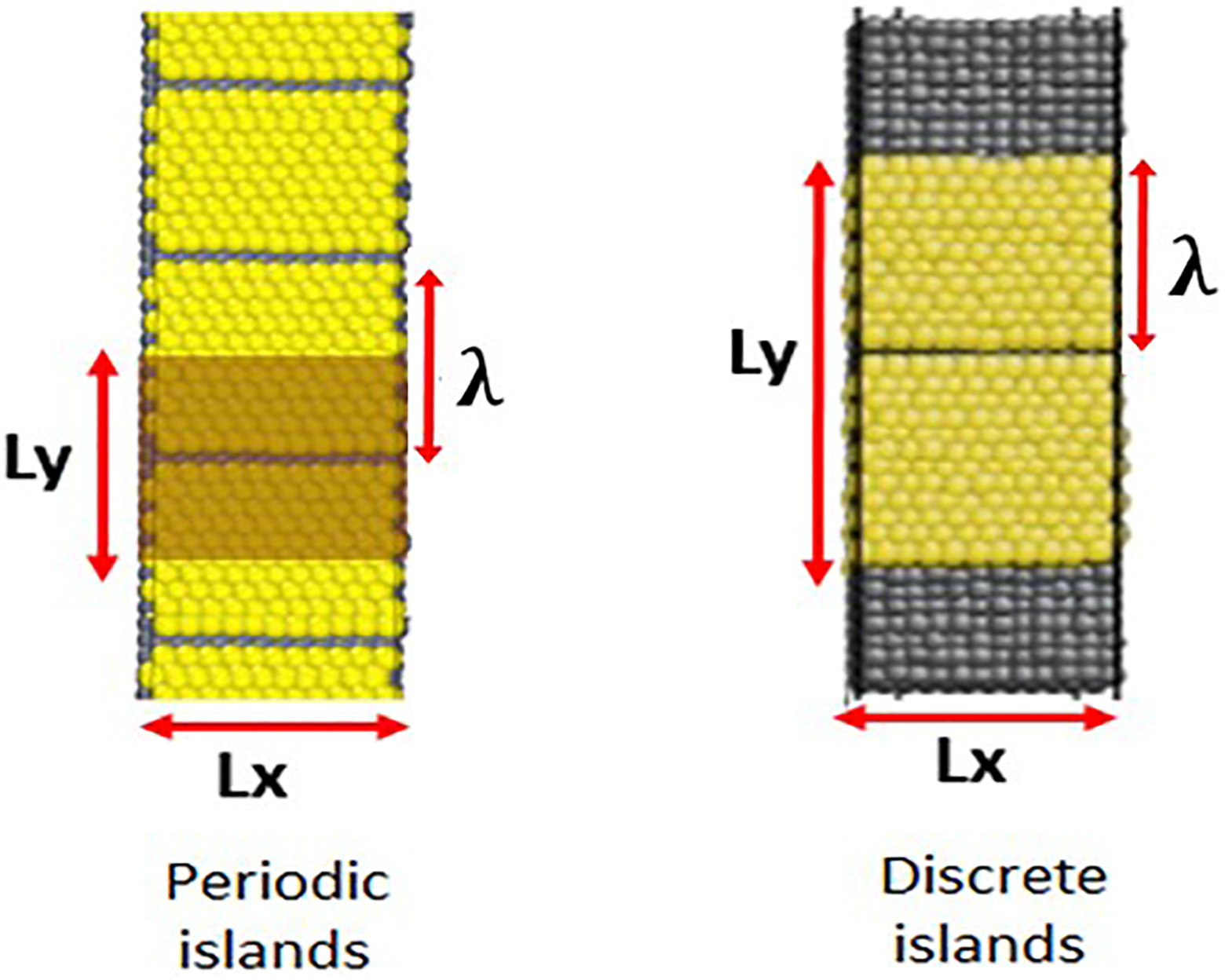
Periodic system and the simulation domain are shown in the shaded region, Ly = λ (left). Discrete island system Ly ≠ λ (right).
In this work, the MD tool (LAMMPS 45 ) computes the energy term given in square brackets in equation (1) and leaves the averaging volume (i.e. (x)) selection to the user where the definition may vary at the surface, around a defect or in the bulk, and so on

This is the simplified version of the virial expression given in the study by Ulz et al. where they included forces due to triple and higher number of atomic interactions in their equation (see equation (1) in the study by Ulz et al.
46
). Here, mi is the mass of atom i, ui is the relative velocity with respect to the mean velocity of the N particle system,
The virial method is used for stress computation in most of the MD simulations due to its simplicity and low computational costs although being less accurate and converging slowly in the domain. 28,47 Recent studies have shown that the virial stress was reported to be out of equilibrium in the vicinity of a defect making the selection of the averaging volume critically important for the consistency of the stress interpretation for that region. 43,44 However, it was also acknowledged that virial results are qualitatively consistent with the macroscopic stress phenomena and thus can be used for visualization purposes for defect simulations. 48
Taking these concerns into consideration, we applied an alternative approach to compute stress on the film using first neighbor spacing data for the film atoms where the local strain was calculated via the difference between the nearest space distances. Using the local strain, Young’s modulus, and Poisson’s ratio, the local stress is computed via equation (2) given in the following (see equation (3.50) in the study by Freund and Suresh 1 ). Here, Hooke’s law applied to the stress on the thin film having its {111} plane parallel to the {001} substrate is given as

where is the misfit strain and C11, C12, and C44 are stiffness coefficients of the stress tensor. Local bond lengths are computed for both the equilibrated full film without defects and the defected film after coalescence. Local strain, ∊mf, is derived taking the defect free film as the reference. Au film layer is in single crystal structure and stress calculations are based on the assumption of anisotropy. Additionally, the film is in plane stress condition where
Before running the simulations for coalescence, preexisting stresses over the full films are recorded after a short run for 100 ps. These data are kept for later analysis to compare the impact of the coalescence process on the existing stress over the film. The preexisting stress was a compressive stress of around 4.5 GPa, as expected due to the mismatch between the relatively large Au film atoms and smaller Ni atoms forming the interface (equilibrium lattice constants at 300 K are computed via LAMMPS to be 4.095 and 3.536 Å, for Au and Ni, respectively). In this work, delta stress (Δσ) values were computed with reference to this preexisting stress on the full film.
Results and discussion
Sub-monolayer growth behavior
Prior simulations indicated that Au on Ni (001) grows at least the first few layers in a layer-by-layer fashion. 43 Indeed, during deposition simulations here, atoms were observed to migrate down at step edges of initially formed 2-D islands (i.e. down Schwoebel hops), whereas no such hops in the opposite sense (i.e. up Schwoebel hops) were observed. In Figures 3 and 4, the relative displacement of the single Au atom (bold color) with respect to the other Au atoms in the cluster is shown in the xy plane.

Delta displacements of the Au cluster atoms and the Au adatom (black circle) inserted at the center of the cluster with respect to the average cluster displacement. Au: gold.

Delta displacements of the cluster atoms and the adatom (black circle) inserted at the edge of the cluster with respect to the average cluster displacement.
An attempt was also made to compute the energy barrier associated with such hops (i.e. the Ehrlich–Schwoebel barrier 44,50 ) for this model. Displacement in the z-direction for the single Au atom and corresponding changes in the potential energy in time is shown in Figure 5, where after 2 ns Au atom hops down to the cluster layer with approximately 1.5 eV drop in potential energy. The negative potential energy of the atom indicates the energy required to remove it from its position. Therefore, a relatively lower potential energy level as occurred during hopping down of the Au atom shows that it is energetically more favorable in the cluster level regarding thermodynamic equilibrium, which also confirms layer-by-layer growth behavior for Au–Ni system. Consequently, ongoing deposition resulted in the formation of single layer islands, which eventually coalesced to form a full monolayer.

Change in the Z coordinate (left axis) and potential energy (right axis) of the adatom during incorporation into the cluster is shown.
The incorporation time of the inserted Au atom regarding its initial position on the cluster was studied via simulation of two cases one of which had the atom centered at the center of the cluster and the other on top of one of the edge atoms of the cluster. Forty-eight different simulations, which started at varying cluster equilibrium times, were run for each case and time distributions are plotted in Figure 6. Although there is not a significant difference in incorporation times for two cases, which were mostly completed in 1–10 ps period, the edge atom is observed to be slightly faster on average. This is an expected result since there are less atoms to be replaced at the edge for incorporation of the atom into the cluster layer.

Incorporation time distributions of the single Au atom inserted at the center versus at the edge of the cluster for 48 different instances for each case. Au: gold.
As a final analysis for this section, the stress behavior during cluster growth has been plotted together with corresponding change in the nearest-neighbor (NN) distance of the Au atoms in the cluster. Figure 7 shows the evolution of stress as a result of the change in NN distance of cluster Au atoms normalized with the NN of the surface Au atoms of bulk Au. Both quantities are plotted against monolayer coverage amounts. A growing compressive stress is observed as cluster approaches to full coverage. This is due to the significant difference between the equilibrium lattice constants for Au and Ni elements. Ni atoms, with smaller lattice constants, in the substrate have caused epitaxial/misfit stress on the overlaying Au atoms, which was compressive. As the deposition continues toward the formation of the second Au layer, the compressive stress is observed to be relaxing due to the incorporation of the second layer Au atoms into the first layer.

Evolution of the NN distance (normalized with respect to the NN Au surface atoms bulk value) and the average stress in the growing cluster. NN: nearest neighbor; Au: gold.
Coalescence stress
Periodic array of islands
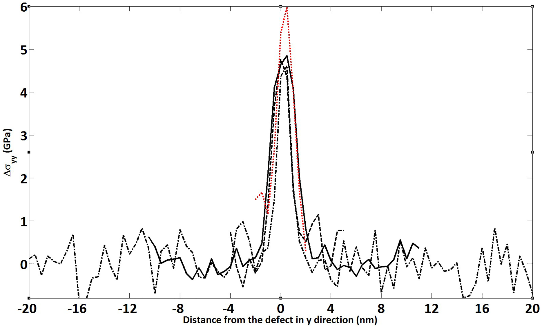
The initial coalescence simulations performed for the 3 × 12 nm2 periodic models were run for 200 ns, which yielded a substantial amount of stress localization around the defected region, which emerged during coalescence of the islands. This stress remained there without any significant changes regarding the width of the stress localization region and the peak stress values attained (see Figure 8) after running the simulation up to 500 ns which was relatively long for an atomic timescale. Stress values shown in the figure are the virial delta stress values of the films relative to the virial stress of the undeformed full Au film on Ni substrate (which was calculated to be around 4.5 GPa compressive stress).

▵σyy stress distributions in the y-direction are shown for Lx = 3 nm with varying Ly ; Ly = 6 nm (solid line), Ly = 12 nm (dotted line), Ly = 15 nm (dashed line), Ly = 21 nm (dashed-dotted line), and Ly = 24 nm (solid-circle).
In order to generalize the spatial and temporal results obtained from this model and to find out about the dependency of the recorded stress manifestation on the geometries, coalescence simulations with different size configurations of Lx and Ly were run for 200 ns. Figure 8 clearly shows the similar behavior in stress localization in both sets which extrapolates to a continuum limit of around 4.8–5 GPa of delta tensile stress.
Looking closer look at the peak stress values for the above-mentioned configurations, it is concluded that size effect is not significant on the peak stress values observed which are confined in the range of 4.5–5 GPa. Similar results were obtained for the models having Ly = 12 nm being fixed with varying Lx sizes. Contrary to the independence of the peak stress and the film size, all coalescence simulation results show that far field delta stress decreases as the film size gets larger (to almost zero for the largest systems).
Finally, width of the stress localization region is computed using full-width half-max method (see Figure 9), where the width of the region subjected to half of the peak stress was taken as the measure for the width of the stress localization region. Like in peak stress behavior, this value was also found to be independent of the system size and it converged to a value of order around 2.5–3 nm with no discernable difference in the continuum limit. This result also explains why no stress localization was observed for our smallest model of Lx = Ly = 3 nm. Since the model size is almost the same as the general width size of the localization region, the localization region has become the entire film itself.
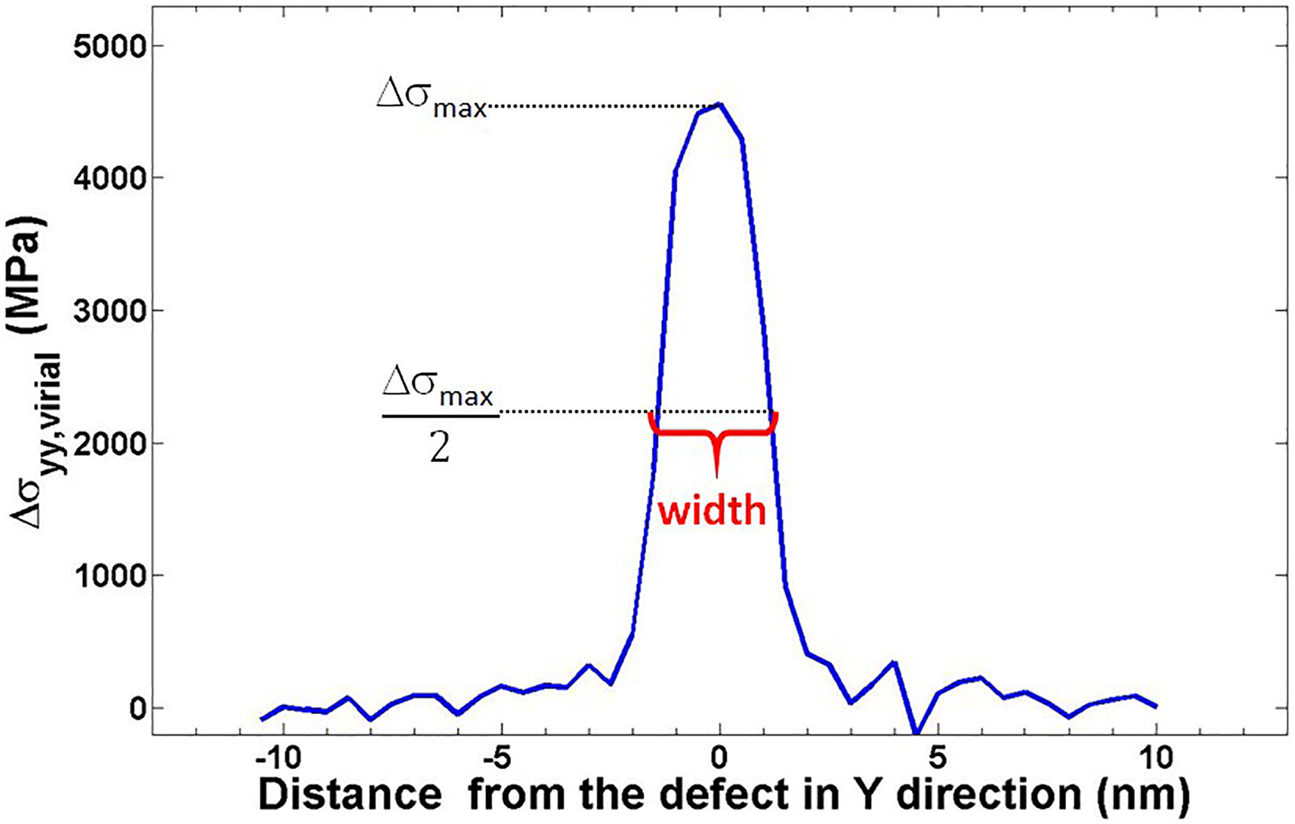
Schematic for the width calculation according to the full-width half-max method (shown on 3 × 24 nm2 sample model).
Alternatively, a deformation analysis was carried, where stress was derived from the local strain data obtained by computing the first neighbor spacing for each atom. Plotting the change in the atomic first neighbor distances for atoms in the full film and in the film after coalescence yielded qualitatively similar results, which also shows strain localization around the initially defected area. Figure 10 depicts the normalized NN distance plotted for Au monolayer for the select 3 × 24 nm2 periodic model (i) when it is on the Au bulk surface, (ii) when it sits on the Ni (001) substrate without any defects in it, and (iii) after the coalescence is completed. NN computed for the Au atoms in the surface layer of its bulk gets narrower when Au monolayer is on top of the Ni (001) substrate, indicating a state of compression. This is parallel to what was found in the simulations as the preexisting stress in the films (i.e. compare plots in Figure 8).
Using the data presented in Figure 10, the average NN values were computed as d Au_bulk = 2.8958 Å for the Au film on bulk surface, d full_ML = 2.8233 Å for the full film monolayer on the Ni substrate, and d peak = 2.9210 Å for the coalesced film occurred at the peak of the localization region. Strain is computed relative to the bulk NN distance of the Au film (∊ full_film = 2.5%, compressed; ∊ coalesced_film = 0.87%, stretched) and substituted into equation (2) as the misfit strain term to calculate associated stress amounts with respect to the bulk state of the Au film.

Normalized NN distance plots for Lx = 3 nm and Ly = 24 nm system with respect to the surface layer NN of the Au bulk (dotted line) are given for Au full film monolayer on Ni (001) substrate (dashed line) and Au film after coalescence is completed (solid line). NN: nearest neighbor; Au: gold; Ni: nickel.
As shown in Table 1, virial stress values are on average 23% less than their corresponding first neighbor results for the coalesced film delta stress case. On the other side, calculations for the existing stress in the full film before defect was introduced yielded similar results. The volume definition in virial stress calculation for the monolayer was criticized for the surfaces, especially in the vicinity of defects where significant stress gradients occur. It was also shown that they produce better results for homogenously deformed regions. 51 This can be the reason for the difference with the MD results. Also note that, for the neighbor spacing calculations, we have used radial distances instead of distance in a single coordinate as x or y and simply substituted the delta value to get the strain which was then used in Hooke’s law in equation (2) to solve for the biaxial stress. But, simulation stress results plotted the normal stress value in the y-direction only (for ▵σyy ). Finally, the reference state for strain calculation is already a deformed state of the Au material (compressed on the Ni substrate) which makes the strain we obtained arguable. Nonetheless, it is worth showing that both approaches qualitatively verified stress localization behavior.
Comparison chart for stress calculations for Ly = 24 nm system via the virial expression and first neighbor distance approach is given.

Discrete monolayer island coalescence
The impact of change in the periodicity of the islands was modeled by removing the periodic boundaries of the models simulated above in the Y-direction and having discrete island counterparts, which are only periodic in the X-direction (see Figure 2).
Coalescence results for 200 ns simulation runs for the discrete islands are displayed in Figure 11, where no significant change relative to the periodic case is observed regarding stress localization occurrence. The peak stress values are computed to be higher for the corresponding models of the periodic islands. However, localized peak stress is observed to decrease down to peak stress levels of the periodic island case as the island size is increased which indicates a transition size in the Y-direction after which islands start to behave like periodic in the Y-direction. This size in Y is estimated to be between 12 and 24 nm, since the peak stress value for the discrete islands of Ly = 12 nm was computed to be 4.8 GPa tension, which was higher than the respective model of the periodic case. It was 4.7 GPa for the Ly = 24 nm case which was slightly lower than that of the periodic counterparts. Localization width values are found to be around 2.4 nm that was around 15% less than the periodic counterparts. Similar to what was obtained in the periodic simulations, each discrete model retained its peak stress and the localization region width without significant changes during further post-coalescence runs.
Discrete islands
As a conclusion, this work herein has demonstrated the evolution of the stress distribution during coalescence process of the manually formed linear defect on the Au monolayer of different geometries. In the first part, periodic islands of different sizes were simulated for coalescence. The most significant finding of the simulations was that dissimilar material interfaces induce a significant effect on stress distribution in thin films that is the stress localization which was observed around the defect region during coalescence and in post-coalescence regime as a residual stress.
Localization region extended to a certain width, which was independent of the system size, being around 2.7 nm. Similar to the width, the delta peak stress values observed in the localized region were also observed to be independent of size, ranging between 4.5 and 5.1 GPa. However, the far field stress was observed to be dropping for increasing system sizes down to the full film, pre-coalescence stress levels.
Stress behavior for coalescence of the defect was also analyzed using deformation data, where changes in the NN distances of the atoms were used to derive strain and stress values. This alternative method yielded results qualitatively matching very well to the direct stress computations of the MD simulations (i.e. occurrence of stress localization around the defect, residual behavior, etc.). However, quantitatively, there was a mismatch where deformation analysis results were higher in magnitude. This can be attributed to the selected volume which was used to divide (pressure × volume) values computed by MD tool to get virial stress. Atomic volume can be hard to define especially in deformed solids or liquids. We defined volume for the stress analysis bins as the product of their width in x, length in y, and an average thickness of the film layer extracted from the density distribution analysis. While the first two dimensions were rigorously defined, the third was not; a rather small value was obtained from density analysis for the monolayer thickness t mono approximately 0.20 nm; however, this is a fairly simplistic interpretation of the spatial extent of the film. If the interaction cutoff distance for the interatomic potentials used here (R c approximately 0.55 nm) is instead used as the thickness, computed stress values are more than halved. Therefore, definitions of film dimensions in atomic scale simulations of thin film growth should be considered more carefully as a part of the future work. However, the outcomes of the virial stress definition, for the surface coalescence of defects, have been shown to be in fairly good agreement with the stress results obtained from deformation gradient analysis. Therefore, local atomistic stress computations can be regarded as a semiquantitative measure.
In parallel to these studies, stress relaxation behavior with additional deposition onto the coalesced film will also be modeled as part of the future work for both periodic and discrete island systems. This work will allow us to see if the localized stress will be relaxed and uniformly distributed over the film or will the stress still exist as film thickness increases.
Footnotes
Declaration of conflicting interests
The author(s) declared no potential conflicts of interest with respect to the research, authorship, and/or publication of this article.
Funding
The author(s) disclosed receipt of the following financial support for the research, authorship, and/or publication of this article: This work was supported by Lehigh University through faculty start-up funding; the authors further acknowledge computing support from Lehigh University's Research Computing support team.