
Abstract
This study reports hydrothermally grown zinc oxide nanorod-based metal-semiconductor-metal ultraviolet detectors with palladium metal as the electrodes. The zinc oxide nanorods were deposited on glass substrates in two steps, seed layer deposition and growth of nanorods. The structural and optical properties of nanorods were examined using scanning electron microscopy and ultraviolet–vis spectroscopy, respectively. The scanning electron microscopy image showed that the growth of nanorods was uniform, and the ultraviolet–vis results indicate that the bandgap of zinc oxide nanorods was 3.23 eV. For metal-semiconductor-metal devices, interdigited metal electrodes with equal interelectrode spacing and a width of 0.3 mm were deposited above the zinc oxide nanorod thin films with a shadow mask using a thermal evaporation system. The current–voltage characteristics of the metal-semiconductor-metal detector were investigated and it showed a contrast ratio of approximately 2.10 and responsivity of approximately 0.199 A/W at 1.8 V. These results are expected to be beneficial to fabricating cheap and practical ultraviolet detection applications.
Introduction
Zinc oxide (ZnO) is a promising semiconductor material for ultraviolet (UV) and blue light detection-based applications such as optically pumped lasers, 1 photodetectors (PDs), 2,3 and light-emitting diodes. 4 Remarkably, ZnO possesses a wide bandgap of approximately 3.37 eV and a large exciton binding energy of 60 meV. 5 –7 In particular, the high optical gain of ZnO has attracted attention for use in sensing and optoelectronics applications. 8 ZnO can be grown as different kinds of one-dimensional (1-D) nanostructures, such as nanocombs, 9 nanorods (NRs), 10 nanobelts, 11 nanoflowers, 12 and nanopillars. 12 These ZnO nanostructures have various applications in optoelectronics, transparent electrodes, and sensors because of their low cost, thermal/chemical stabilities, radiation hardness, and high transparency in the visible range. 13 Among these various morphologies, 1-D ZnO NRs have recently attracted significant attention because of their special shape and structure, which results in excellent piezoelectric, magnetic, and optoelectronic properties. 14,15 There are several deposition techniques for the growth of 1-D ZnO NRs, such as thermal evaporation, 16 carbothermal synthesis, 16 radio frequency magnetron sputtering, 17 molecular beam epitaxy, 18 sol–gel process, 19 hydrothermal, 20 and chemical vapor deposition. 20 Among these methods, the hydrothermal method is commonly used because it is simple and cheap. 20 –23 Recently, several studies have been performed on UV PDs using ZnO NRs fabricated using the hydrothermal method as well as other growth techniques. 22,24 –26 Zhilin et al. reported the photoelectric characteristics of ZnO NR-based metal-semiconductor-metal (MSM) UV detectors. 16 They deposited ZnO NR thin films using two different methods. The first one was a catalyst-free carbothermal synthesis and the second was a catalyst-free thermal evaporation of metallic zinc. They used gold (Au) metal electrodes for their MSM devices and reported photosensitivity values of 97 mA/W at approximately 325-nm illumination and 44 mA/W at approximately 518-nm illumination at a bias of 5 V, for their MSM UV detectors. 16 Lee et al. reported hydrothermally grown ZnO NR-based near-UV PDs with an MSM structure. They used silicon dioxide/silicon as substrates and an aluminium-doped ZnO thin film as a seed layer. Conventional photolithography was used for the fabrication of MSM structures, and titanium/Au was used as the metal electrodes. 24 Although many research groups are working on ZnO MSM UV PDs, there are very few studies on hydrothermally grown NR-based MSM UV detectors. Most of the research groups have used Au as the metal electrode for their MSM UV detectors. 16,24 –27 In this study, we have used palladium (Pd) metal electrodes for NR-based MSM UV detectors for the first time because of its high work function (approximately 5.2 eV) and thermal/chemical stability. We used a shadow mask for the deposition of Pd metal electrodes, which is a relatively convenient and easy fabrication technique compared to previously reported studies on ZnO NR-based MSM UV PDs.
Experimental method
Figure 1 shows a schematic illustration of the fabrication steps of ZnO NR-based MSM UV detectors. Some glass slides of size approximately 1” × 1” were used as substrates in the experiment. In the first step, the glass slides were cleaned ultrasonically using acetone and methanol, then rinsed with deionized (DI) water, and finally dried using a nitrogen blowgun. In the second step, a seed layer of pure ZnO was deposited on the glass substrates. In the third step, the ZnO NRs were grown above the seed layer. After that, samples were covered with shadow mask, for depositing Pd metal of approximately 100 nm thickness by thermal evaporation.

Schematic illustration of the fabrication steps of ZnO NR-based MSM UV detectors. ZnO: zinc oxide; NR: nanorod; MSM: metal-semiconductor-metal; UV: ultraviolet.
The precursors used for the ZnO seed layer solution were zinc acetate dehydrate powder (Zn(CH3COO)2·2H2O) and ethyl alcohol (C2H6O). The precursors used for ZnO NR solution were zinc nitrate hexahydrate (Zn(NO3)2·6H2O), hexamethylene tetramine (C6H12N4), and DI water. The concentration of the ZnO seed layer solution was 60 mM and the concentration of the ZnO NR solution was 30 mM. The seed layer solution was stirred with a magnetic bar at a temperature of 80°C for 1 h, whereas the ZnO NR solution was stirred at a temperature of 90°C for 1 h. Further details about the growth of ZnO NRs by the hydrothermal method can be found elsewhere. 10,23,28
After the deposition of the interdigited Pd metal electrodes, the current–voltage (I-V) characteristics of the ZnO NR-based MSM devices were investigated under dark and UV light conditions. A lamp with a wavelength of approximately 365 nm and an incident optical power of approximately 650 μW were used as the UV light source. The I-V characteristics of the ZnO NR-based MSM UV detectors were measured using a semiconductor parameter analyzer (Agilent B1500A). Figure 2 displays ZnO NR-based MSM devices under UV light conditions.

Schematic illustration of ZnO NR-based MSM devices under UV light. ZnO: zinc oxide; NR: nanorod; MSM: metal-semiconductor-metal; UV: ultraviolet.
Results and discussion
Structural characterization
Figure 3 shows the scanning electron microscope (SEM; HITACHI S-4800, Japan) image of ZnO NR films grown on glass substrates. The SEM image confirms that the growth was uniform and the NRs were aligned well normal to the substrate. The top surface of the NRs was hexagonal in shape. 29 The average diameter of the NRs was 45 nm and the average length of the NRs was 1 µm (obtained from cross-sectional SEM, shown as inset).
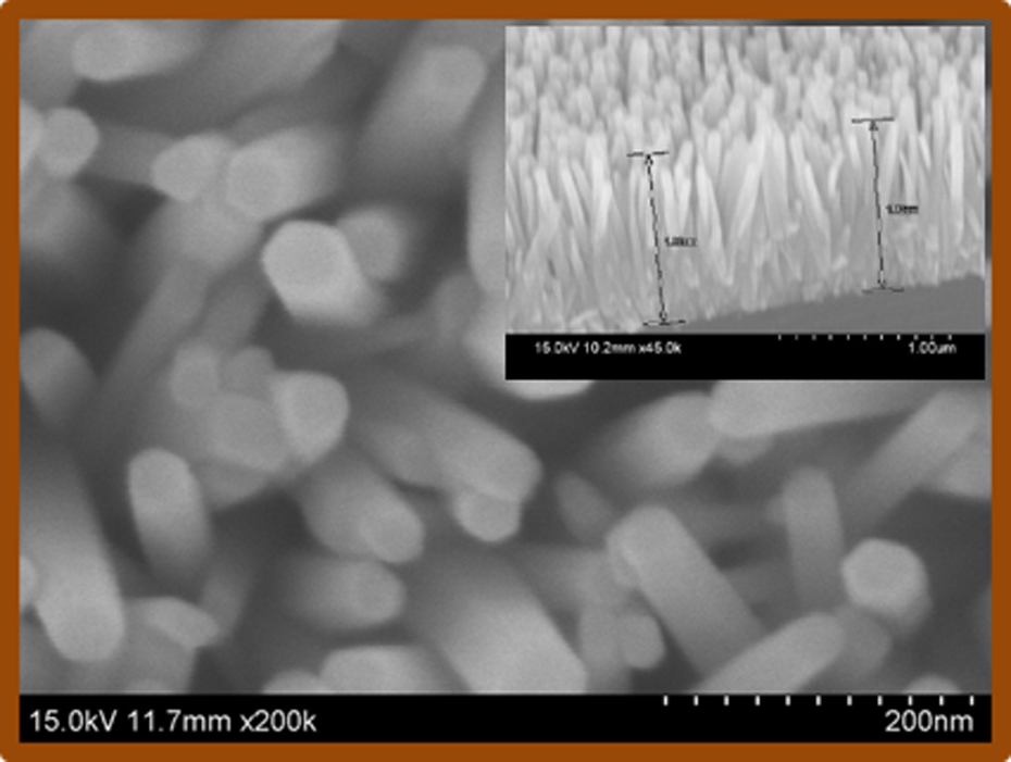
SEM image of ZnO NRs grown by the hydrothermal method. SEM: scanning electron microscopy; ZnO: zinc oxide; NR: nanorod.
Optical characterization
UV–vis spectroscopy of ZnO NR thin films on glass substrates was performed using a Cary-5000 system (Agilent Technologies, USA). Figure 4(a) shows the absorbance spectra of ZnO NR thin films. It can be seen from the figure that the absorbance mainly occurs over a wavelength range of 350–375 nm. The bandgap of the ZnO NR thin films can be calculated from these absorbance spectra. The expression for determining the optical bandgap of ZnO NR thin films is as follows 30
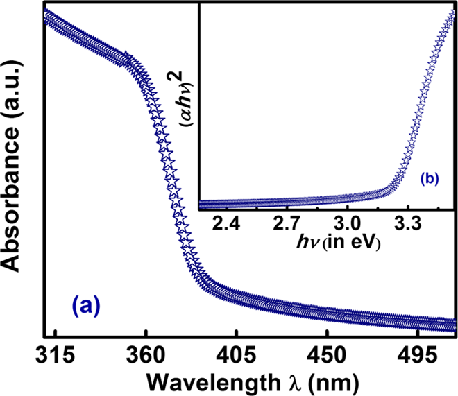
UV–vis results for ZnO NR thin films. (a) Absorbance spectra. (b) Bandgap calculation. UV: ultraviolet; ZnO: zinc oxide; NR: nanorod.
where hν is the photon energy, α is the absorption coefficient, and B0 is a constant. The optical bandgap Eg could be extracted from the (αhν)2 versus hν curve. 30 The calculated value of the bandgap for our ZnO NR thin films was 3.23 eV. The X-ray diffraction patterns of the NRs indicated that the NRs grown in single phase with a wurtzite structure (not shown here).
Electrical characterization
Figure 2 shows a schematic illustration of the ZnO NR-based MSM devices under UV light. The I-V characteristic of the ZnO NR-based MSM devices was measured in the dark and under UV illumination, as shown in Figure 5(a) and (b). An MSM device consists of interdigited Schottky contacts connected back to back. 31 It can be seen clearly from Figure 5(a) that the I-V characteristics of our ZnO NR-based MSM devices are nonlinear, which confirms the formation of Schottky contacts between the metal (Pd) and the semiconductor (ZnO NRs), in accordance with the Schottky–Mott theory. 32 The I-V relation of these ZnO NR-based MSM detectors can be described as follows 31,33 :


(a) Linear I-V characteristics and (b) log I-V characteristics of ZnO NR-based MSM UV detectors measured under UV and dark light. I-V: current–voltage; ZnO: zinc oxide; NR: nanorod; MSM: metal-semiconductor-metal; UV: ultraviolet.
where IS is the saturation current, T is the absolute temperature, V is the applied voltage, q is the charge, η is the ideality factor, and k is the Boltzmann constant. The saturation current (IS ) can be expressed as

where A* is the effective Richardson constant, A is the Schottky contact area, and qϕ B is the Schottky barrier height. 31,33
It can be seen from Figure 5(a) that at an applied bias of 1.8 V, the value of the dark current was 6.16 × 10⁻⁵ A and the value of the photocurrent was 1.29 × 10⁻⁴ A. In other words, the photocurrent was about two times higher than the dark current. The responsivity of the ZnO NR-based MSM detectors can be calculated from the following relation 34 :

The values of the responsivity and the contrast ratio were calculated from the graph using these equations. All the values for the ZnO NR-based MSM detectors are summarized in Table 1. Although the values for the contrast ratio and responsivity were not very good, further optimization of the growth conditions and other factors related to fabrication can improve these parameters. We believe that the sensitivity of these hydrothermally grown ZnO NR-based MSM devices would be good enough for UV detection applications.
Detailed parameters of ZnO NR-based MSM UV detector obtained from the I-V characteristics.

Pd: palladium; ZnO: zinc oxide; NR: nanorod; MSM: metal-semiconductor-metal; UV: ultraviolet; PD: photodetector.
Theory of photodetection of ZnO NRs
When UV light falls on ZnO NRs, absorption of photon occurs, and these absorbed photons create pairs of electrons and holes. The generation of e − h pairs at the surface of ZnO NRs is directed by the adsorption and desorption of oxygen molecules (O2). 35 This process can be expressed as follows 36 :


Here, equation (5) shows the absorption of oxygen molecule, equation (6) shows the generation of electron–hole pairs, and equation (7) shows the hole trapping phenomenon through oxygen adsorption and desorption. The details of the photodetection theory for ZnO NRs are explained elsewhere. 36,37
Conclusion
Hydrothermally grown ZnO NR-based UV detectors with an MSM configuration were fabricated on glass substrates. Pd was used as the electrode metal for the MSM devices. The crystal and optical properties of the ZnO NRs were investigated by SEM and UV–vis spectroscopy. The SEM images showed that an array of high-density ZnO NRs was grown on the glass substrate. From the I-V characteristics, it was observed that the value of the photocurrent was twice that of the dark current. The responsivity and contrast ratios were 0.19 and 2.10 A/W, respectively, for the MSM detectors. These results provide greater insight into the design and simple fabrication of MSM detectors for various optoelectronics applications.
Footnotes
Declaration of conflicting interests
The author(s) declared no potential conflicts of interest with respect to the research, authorship, and/or publication of this article.
Funding
The author(s) received no financial support for the research, authorship, and/or publication of this article.