
Abstract
It is essential for flapping-wing micro aerial vehicles to have a driver with compact size, low mass, and high conversion efficiency in low-power application. In this article, a dual-stage low-power converter driving for piezoelectric actuator was designed and implemented, which can be applied in flapping-wing micro aerial vehicles. Using the “simultaneous drive” method, an Residual Current Devices (RCD) passive snubber flyback DC/DC step-up converter cascaded with a bidirectional active half-bridge drive stage is designed. The flyback converter is controlled by pulse width modulation in discontinuous conduction mode to ensure the stability of the output high voltage. The half-bridge drive stage takes the approach of comparing the output voltage signal with an ideal waveform lookup table to generate arbitrary unipolar signals. The proposed converter has a weight of 345 mg, a size of 285 mm2 (19 × 15 mm2), a maximum output power of 500 mW, and a maximum conversion efficiency of 64.5%. An experiment driving for piezoelectric actuator was performed to observe the displacement generated by the converter. According to the experimental results, this converter can be applied in flapping-wing micro aerial vehicles.
Keywords
Introduction
Compared with conventional unmanned micro aerial vehicles (MAVs), flapping-wing MAVs (FWMAVs) possess compact size, good operability, light mass, and so on. 1 Therefore, they have very attractive application prospects in both military and civilian fields. Mineta et al. considered a complete fabrication solution for actuators, links, flexures, integrated wiring, and structural elements using high-performance materials. 2 The core of kinetic energy of FWMAVs and smart actuators is generally made of piezoelectric materials, which have high conversion efficiency and sufficient deformation strength compared to mini electric motors. 3,4
The driving circuit of piezoelectric materials generally needs to meet two requirements. Firstly, the generation of a high-voltage driving signal from a low-voltage power supply is required, which can drive the piezoelectric materials to obtain sufficient displacement. 5 Secondly, unused energy should be recovered from piezoelectric materials, because only a portion of the input electrical energy is converted into mechanical deformation, and the rest is stored in the drive circuit. 2,6 Therefore, it is of great significance to investigate compact drive circuit with high energy efficiency and high-power density, which is beneficial for the efficiency improvement of FWMAVs.
Meanwhile, the matching voltage conversion circuits should be designed to satisfy the electrical requirements of piezoelectric actuators (PZTs). 6 Several researchers have discussed the miniaturization of voltage conversion circuits for microrobotic applications. A boost converter cascaded with a switched capacitor circuit was adopted by Steltz et al. to obtain high voltage. 7 However, this structure requires a large number of pump capacitors, which increases the size of the circuit and reduces its power density, particularly at a high output power. Other topologies with more components and a high step-up ratio are also suitable for driving high-voltage reactive loads; however, most efforts have focused on large-scale and high-power applications. 8 –10 In another part of the circuit, a simple push–pull driver described by Steltz et al. 7 can generate a unipolar square wave voltage across the load without energy recovery. The majority of existing topologies focus on efficient piezoelectric driving for large-scale and high-power applications, which reduces the efficiency and power density of the power supply. 3,11 –15 Harvard’s team has previously produced a small-scale power conversion interface. However, as described by Karpelson et al., 16 the boost tapped-inductors they use have difficulty in manufacturing compared to general flyback transformers. At the same time, in the DC-AC stage, the detection of current becomes quite difficult in the case of low power. This article is dedicated to improving and validating the short board mentioned above.
In this article, a dual-stage low-power converter driving for PZT was designed and implemented. An RCD passive snubber flyback DC/DC step-up converter cascaded with a bidirectional active half-bridge drive stage is designed. The proposed converter has a weight of 586 mg, a size of 169 mm2 (13 × 13 mm2), a maximum output power of 500 mW, and a maximum conversion efficiency of 64.5%. An experiment driving for PZT was performed to prove that the driving converter can be applied in FWMAVs.
This rest of the article is organized as follows. The second section introduces the driving requirements and strategies for PZT. The third section presents the design and control of the drive converter. The fourth section describes the fabrication specifications and experimental realizations of the converter. Finally, the conclusion of the study and directions for future research is provided in the last section.
Driving requirements and strategies for PZT
Drive requirements
In order to drive a single morph PZT, the single-pole drive signal can be directly connected to the electrode of PZT, as shown in Figure 1(a). The direction indicated by the arrow is the direction of polarization. Figure 1(b) and (c) shows two driving methods of bimorph PZT with a unipolar drive signal. 17 The driving method shown in Figure 1(b) is known as “alternate drive method” which includes two unipolar drivers with phase difference of 180° and common ground connected to the central electrode of PZT. In Figure 1(c), the driving method is called “simultaneous drive method” that consists of a constant high DC voltage applied to external electrode of PZT and a single-pole drive signal connected to the central electrode of PZT. The “alternating drive method” requires 2n drive signals for n bimorph PZTs, while the “simultaneous drive method” mode allows n bimorph PZTs to share one high DC voltage. Therefore, “simultaneous drive method” can achieve the use of n drive signals and one high DC voltage to drive n bimorph PZTs, and the driving architecture is relatively simple correspondingly. 18
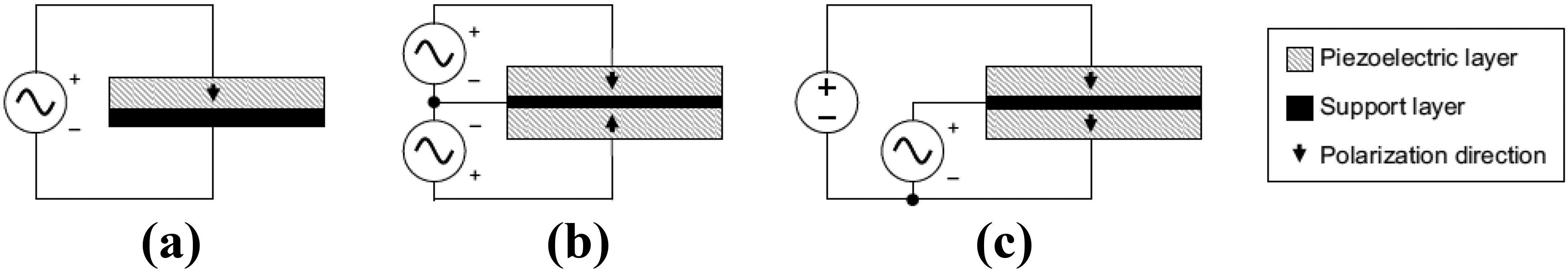
Drive modes of PZT. PZT: piezoelectric actuator.
From the point of view of designing electronic circuits, the variable driving signal can be realized via two methods, namely, single-stage driving method and two-stage driving method. The single-stage driving method achieves both boost function and drive function. The first stage of the two-stage driving method converts low DC voltage into high DC voltage, and the second stage converts high DC voltage into time-varying driving signal. Because the two-stage driving method has a constant high bias voltage, it is well suited to the driving architecture, as shown in Figure 1(c), while the single-stage driving method is commonly used in the cases of Figure 1(a) and (b). Two-stage driving method can support a high bias voltage, but has a larger volume and heavier mass than single-stage driving method. Therefore, the choice of driving architecture depends on the type and quantity of PZTs.
Except to generate drive signals satisfying exciting request, the driver should also meet other two important requirements. Firstly, the driver should be able to generate arbitrary signal waveforms to enhance the versatility in different applications. Secondly, the unused electrical energy from the PZTs can be recovered to raise conversion efficiency.
Equivalent model of PZT
In order to match the electrical performance of PZTs, the equivalent model should be investigated firstly. In this study, the equivalent model of bimorph PZTs proposed by Karpelson et al. is adopted 19 ; the model is shown in Figure 2.

Equivalent model of bimorph PZTs. PZT: piezoelectric actuator.
The equivalent model includes a static part and a series of mechanical resonance branches. The static part consists of equivalent capacitance C 0, dielectric loss Rp , and hysteresis loss Rs . Different mechanical resonance branches correspond to different mechanical resonance modes. In each branch, inductance Ln , capacitance Cn , and resistance Rn represent the equivalent mass, elastic coefficient, and damping coefficient, respectively. According to the equivalent model, the static part, the resonance branch, and the total impedance can be expressed as


The bimorph PZT (QDTE52-7.0-0.82-4; PANT, Suzhou, China) used to test dynamic performance has the following parameters: 190 V highest driving voltage, 52 mm long, 7 mm wide, 0.82 mm thick, and 1.2 mm bidirectional displacement. The first resonant frequency is approximately 100 Hz close to the driving frequency of an insect-type robot, which makes the research practical.
The impedance characteristics of the material were measured using an Agilent 4294A impedance analyzer. We can fit the experimental curve by choosing the values of the electronic components. Figure 3 shows the measured frequency response of used bimorph PZT and model frequency response is theoretically calculated with MATLAB.

Impedance characteristic of used bimorph PZT. PZT: piezoelectric actuator.
It can be seen from the comparison result that the used bimorph PZT has four resonant frequencies, from 100 Hz to 30 kHz. Hence, the equivalent model has four LCR branches. The first resonant frequency is nearly 121 Hz that conforms to the flapping frequency of the wings of FWMAVs. The parameters of the equivalent model are illustrated in Table 1.
Equivalent parameters of the used bimorph PZT. PZT: piezoelectric actuator.

PZT: piezoelectric actuator.
Besides, due to the hysteresis effect of the bimorph PZT, the nonlinear mechanism cannot be completely expressed by linear circuit element. For a given operating voltage and frequency conditions, the hysteresis loss can be approximated by reasonably selecting the parameters of the equivalent circuit.
Design and control of the drive converter
The flyback RCD clamping circuit (DC-DC stage) cascaded with bidirectional active half-bridge drive circuit (DC-AC stage) is used to constitute the dual-stage drive converter, 12,20 as shown in Figure 4.
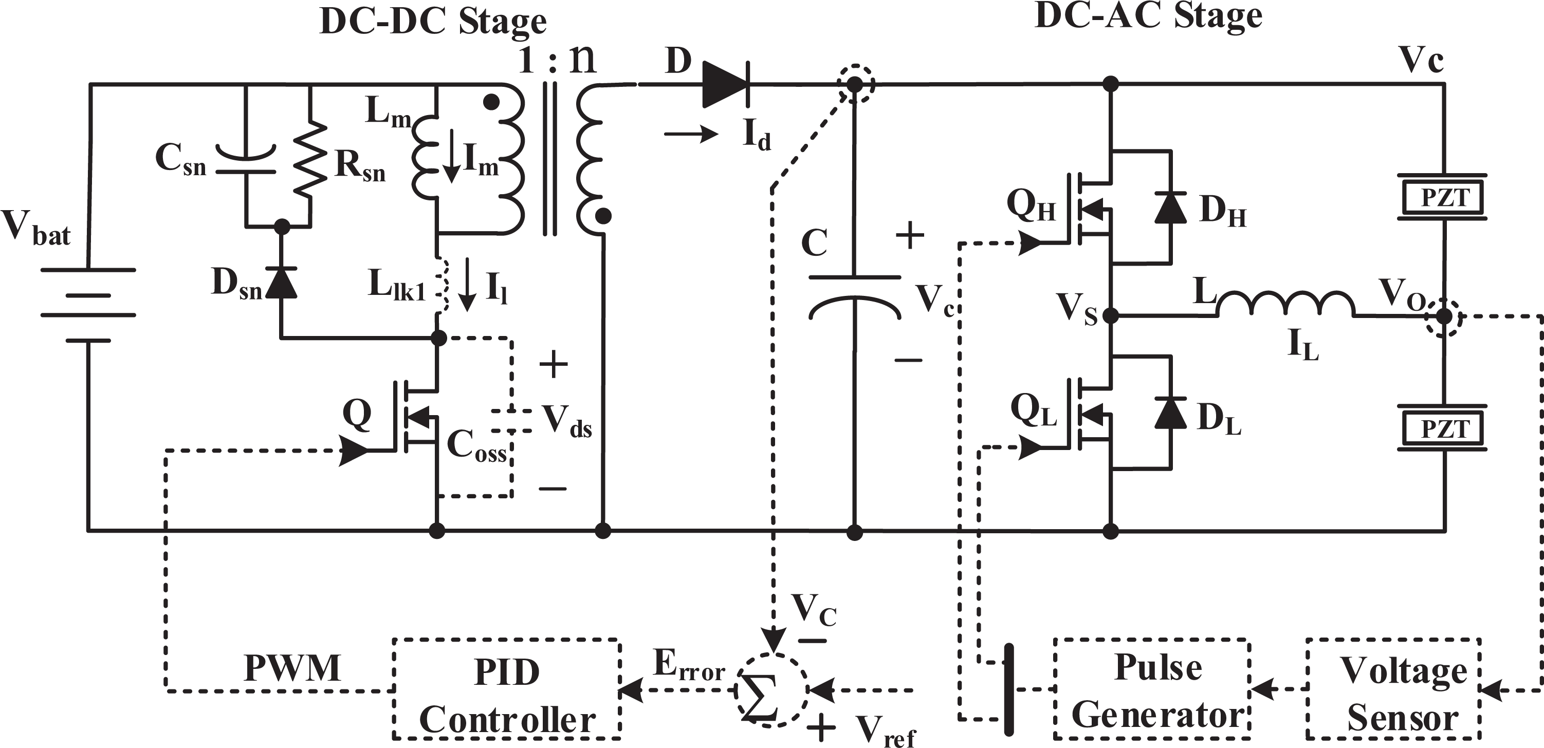
Dual-stage drive converter.
The step-up DC-DC stage is controlled by the pulse width modulation method. Because the equivalent resistance of the load is low, the stage works in discontinuous conduction mode (DCM), which is capable of high step-up conversion ratio. The bidirectional active half-bridge drive circuit can generate variable single-pole drive signals within a certain frequency range and can recover unused electrical energy from PZT load to improve the energy conversion efficiency. Compared with other DC-AC converters, the bidirectional active half-bridge drive circuit has smaller volume and higher power density. The drive converter can generate two exciting signals to meet the driving requirements of bimorph PZT via using a simple control strategy. The working principle and control method of proposed drive circuit are introduced in detail in followed contents.
Step-up DC/DC stage
As shown in Figure 5, the step-up DC-DC stage is a flyback converter with RCD clamping circuit, which is very suitable for low-power applications.
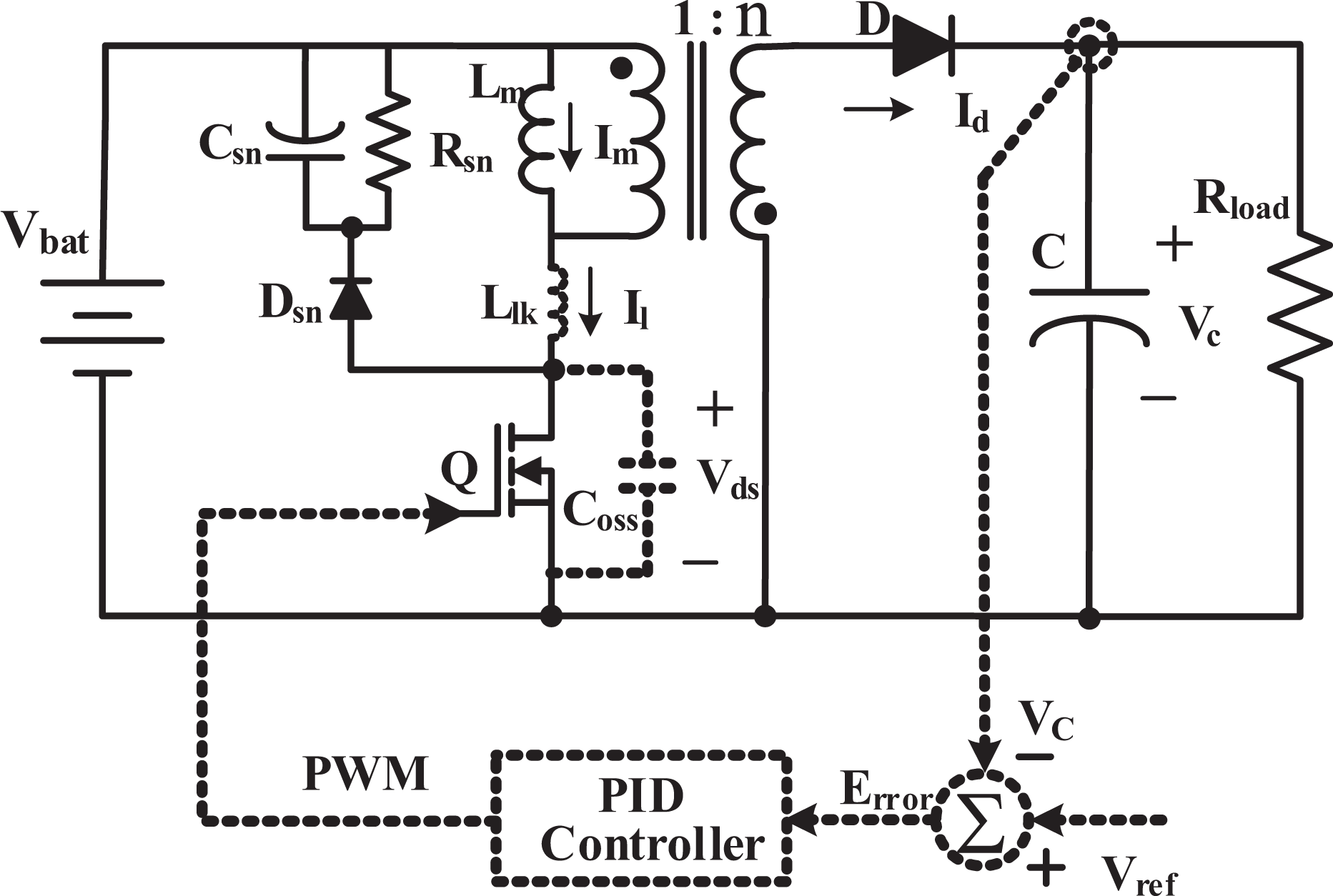
Step-up DC-DC converter.
Compared with forward converter, the mentioned converter does not have secondary output inductance, so the advantage of more compact volume is improved significantly. The converter works in DCM, which has many advantages compared to continuous conduction mode, such as more simple control, higher efficiency, and higher step-up ratio. 8
The voltage and current waveform of flyback converter in one operating cycle is shown in Figure 6.
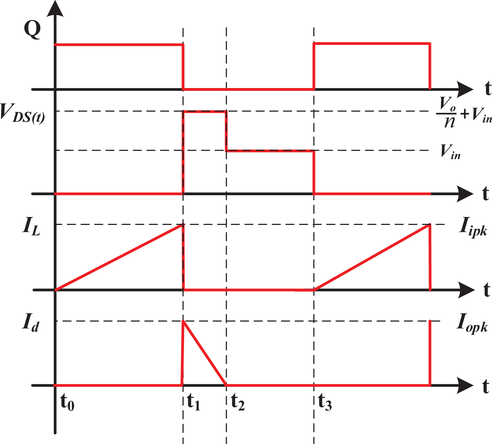
Voltage and current waveform flyback works in DCM. DCM: discontinuous conduction mode.
As shown in Figure 6(a), when the switch Q is turned on, the primary current IL starts to build up under the action of the power supply and energy is stored in the magnetizing inductance Lm . When switch Q is turned off, the energy stored in the transformer starts to transmit to the secondary side through magnetic coupling and the rectifier diode D, thereby outputting a high DC voltage.
The voltage step-up gain in DCM mode is given by

where Vc and V bat are the input and output voltages, respectively. D is the controllable on-time duty cycle, n is the transformer turn ratio, R is the equivalent load impedance, which represents the impedance of the half-bridge converter and the capacitive loads, Lm is the magnetizing inductance of the transformer, and fs denotes switching frequency.
In practice, when the switch Q starts to turned on, surge current appears on the primary side of transformer, which is caused by the rectifier diode D. At the moment when switch Q is switched off, short-term resonance will be happened between the leakage inductance of transformer and the equivalent parasitic capacitance of switch Q. At this time, the voltage applied on the switch Q has a sharp peak. In order to guarantee the switch Q works normally, a protective circuit must be adopted to suppress the sharp voltage in a safe range; otherwise, the switch Q will be irreparable damaged.
In Figure 5, L lk is the leakage inductance of the transformer. When the switch Q is closed, V bat voltage is applied to the primary inductance of transformer. Because the diode D sn is reverse biased, which prevents the charging of capacitor C sn, C sn discharges through the resistance R sn. When Q is switched off, the parasitic capacitor C oss is charged by the current of the primary side due to the flyback effect, and V oss rises gradually. When V ds rises to V bat + V csn, the diode D sn in the clamping circuit is positive biased, and the current is shunt by C sn and R sn. At this time, V ds is clamped at V bat + V csn. Because parasitic capacitor C sn is much larger than parasitic capacitor of switch Q, the excitation current almost all through the C sn. When the reverse voltage of transformer rises up to Vc , the current stored in primary side of transformer suddenly transfers to secondary side of transformer, and voltage of primary side of transformer is clamped at Vc/n. At this time, as the current in the leakage inductor L lk cannot be mutated, the current will continue to charge the clamping capacitor C sn until the current of the primary side inductor becomes zero and the clamping circuit of RCD stops working.
DC-AC drive stage
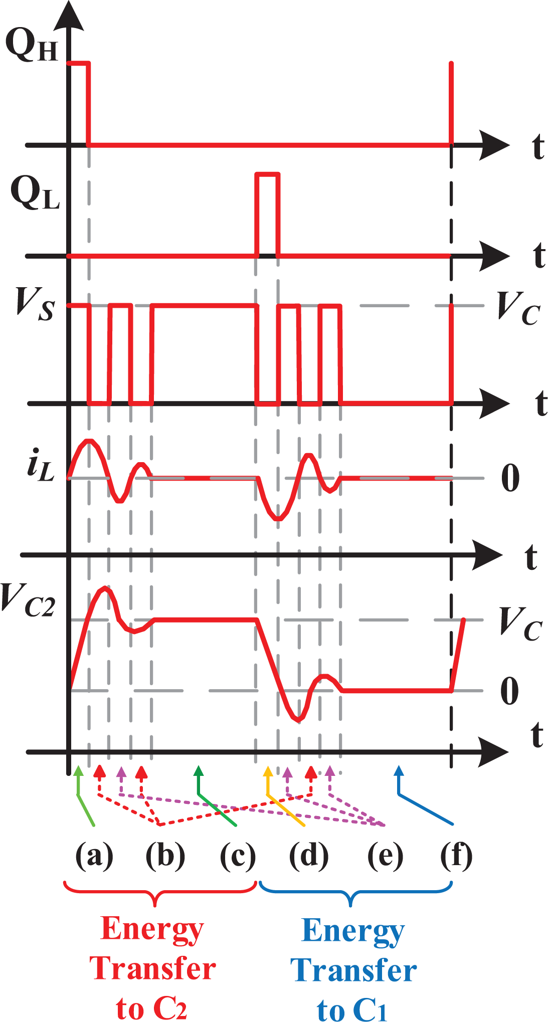
The bidirectional active half-bridge drive circuit converts high DC voltage outputted by DC-DC stage to high amplitude and high frequency signal which can drive the bimorph PZT. 15 The drive circuit consists of an inductor with high quality factor and two inherent capacitors of bimorph PZTs; the different operating modes are shown in Figure 7.

Different operating modes.
In mode (a), when switch QH is switched on, the inductance current iL begin to rise, and the high-side equivalent capacitance C 1 of PZTs starts to transfer the unused energy to the low-side equivalent capacitance C 1. If equivalent series resistance in the circuit is taken into account, according to Kirchhoff’s voltage law (KVL), the following equations can be obtained

Combing two above equations, a second-order differential equation can be obtained

Where
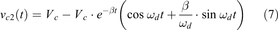
The driving voltage signal is an underdamped voltage that attenuates oscillation at an angular frequency
In operating mode (b), once the switch QH is turned off, the inductance current iL begins to decrease via diode DL . A new oscillation begins between the inductance L and the equivalent capacitance C 2. According to KVL

In underdamped oscillation condition

Where
In mode (c), the low-side piezoelectric drive capacitance is fully charged, while the high-side equivalent capacitance C 1 is completely discharged to zero. The drive signal is the same as Vc , and all unused energy is transferred from the high-side capacitor C 1 to the low-side capacitor C 2, thus energy efficiency is improved.
When the switch QL is switched on, the mode (d) starts to open. Similarly, the unused energy of the lower side capacitor C 2 transferred to the higher side capacitor C 1. Due to the discharge of capacitor C 2, the inductive current iL starts to increase in reverse direction. Similarly, Vc 2 is calculated as follows

Operating mode (d) is over when the voltage Vc 2 is reduced to zero. Similar to mode (b), when QL is off, the current iL continuously passes through the diode DH , and the circuit operates in mode (e). In mode (e), the initial voltage of the capacitor Vc 2 is zero, which can be calculated as

where
Mode (f) is similar to mode (c). All the energy stored at low-side capacitor C 2 is transferred to the high-side capacitor C 1 and equals to Vc .
Figure 8 illustrates the switching pulse waveform (QH and QL ), leakage voltage V ds, current iL , and output voltage Vc 2 in a complete working cycle. In a complete working mode sequence (a)-(b)-(c)-(d)-(e)-(f), modes (a) and (d) are the beginning of each half-period, respectively; modes (b) and (e) are the oscillation of each half-cycle, respectively; and modes (c) and (f) are the voltage stability stage in each half-period, respectively.
The waveforms in one complete working cycle.
By sending a series of control signals to QH and QL , any drive signal waveform can be generated in Vc 2. This circuit only transmits a small amount of energy in each working cycle, so that a small-sized inductance can be used. 10
Experimental validation
Fabrication specifications
The circuit topology described in Figure 4 is soldered onto a well-designed printed circuit board (PCB) using discrete components. Table 2 lists the specifications of the discrete components, which include two MOSFETs, a diode, a flyback transformer, a capacitor, and a resonant inductor. The step-up DC-DC stage is responsible for increasing the input DC voltage. The basis of the selection is to ensure that the components can handle the predicted voltage and current without breakdown and failure.
The detailed parameters of circuit components.

Table 2 describes the detailed parameters of elements used in drive circuit.
Flyback converter is responsible for increasing the input DC voltage, mainly including power MOSFET, rectifier diode, flyback transformer, and filter capacitor. The main consideration of the choice is that the device will not be broken to guarantee the drive circuit works safely and stably. As mentioned above, the input voltage varies in the range of 3.0–4.5 V, and the maximum value of the average current can reach up to 200 mA. Therefore, when the output is approximately 100 V, the average output current should be less than 10 mA. The N-channel enhanced MOSFET SI2304 encapsulated in sSOT-23 is selected in DC-DC stage, which has enough endurance for high voltage and sufficient compactness. It has a maximum current of 2.6 A and voltage of 30 V. When the gate source voltage V GS is 4.5 V, the measured leakage resistor is 55 mΩ, so it is capable of low conduction loss.
The rectifier diode adopts Schottky diode SMD1200PL with SOD-123 package, which can withstand an average forward current of 1 A and a maximum reverse voltage of 200 V. Compared with the traditional diode with a conduction voltage of 0.7 V, the voltage of SMD1200PL is only 0.4 V, while the forward current is 20 mA, which is key consideration for chip selection.
The flyback transformer CJ5143-AL is produced by COILCRAFT company, which has excellent coupling coefficient (>0.95) and good electromagnetic interference performance. Its primary inductance is 15 μH and the turn ratio is 1:15. The coupling inductance can handle the peak current of 1.2 A without saturation. The output filter capacitor is a 1 μf/110 V ceramic capacitor encapsulated with 0603 package.
In DC-AC stage, N-channel-enhanced MOSFETs TN2404 K with SOT-23 package are used for both high-side switch and low-side switch that has a voltage endurance up to 240 V and low on-off resistance. The inductor has high quality factor and is encapsulated with 0603 package. According to the design criterion, the inductance should be as small as possible to increase the resonance frequency. In addition, the high quality factor also reduces the power loss of the drive circuit.
Using the above components, a prototype was fabricated. The physical image of the fabricated circuit is shown in Figure 9.

The physical image of drive circuit.
The dual-stage driving circuit is composed of Surface Mount (SMT) discrete components welded on the designed PCB. The drive circuit has a mass of 345 mg and a size of 19 × 15 mm2.
Circuit experimental validation
The drive circuit uses low voltage of lithium battery as energy input to generate high voltage. The input voltage of the drive circuit is 3.7 V, and the output voltage can reach up to 100 V; 1.5 MΩ resistor is used as pseudo load to replace bimorph PZT in circuit performance test experiment. The results show that the drive circuit has 0.5 W output capacity.
Using the aforementioned half-bridge closed-loop control method, the drive circuit can generate sinusoidal waveform, as shown in Figure 10.

Sinusoidal drive signal.
Figure 10 shows the control waveforms of high-side switch QH (red color) and low-side switch QL (green color). In drive voltage rise stage, the high-side switch QH keeps switching on and off, the inductor L resonates with the low-side capacitor C 2 load, the low-side capacitor C 2 keeps charging, and the drive voltage rises. At this time, the low-side switch QL is off. Similarly, in drive voltage drop stage, the high-side switch QH is switched off, while the low-side switch QL continues to work. The low-side capacitor C 2 begin to discharge and transfer the energy to high-side capacitor C 1, so as to output a complete period of sinusoidal signal. As seen in the right enlarge figure, the high-side switch QH is open when the low-side capacitor C 2 reaches the target voltage, which can avoid the unnecessary switching action, greatly reduce the switching loss, and improve the circuit conversion efficiency. In addition, different drive voltage waveforms can be achieved to display the universality of drive circuit.
The energy efficiency of the drive circuit can be simply expressed as

Where P load is the average power of the load and P in is the average input power. Figure 11 shows the efficiency of the drive circuit topology under different loads and different output signal frequencies.

The relationship between conversion efficiency and load under different driving frequencies.
The measured loads range is from 10% to 100% with an interval of 10%. The three driving frequencies are 5, 10, and 15 Hz, respectively. It can be seen from the measurement that the peak efficiency (64.5%) is achieved under 60% load and 5 Hz driving frequency, which is higher than the maximum conversion efficiency of 42.4% obtained by Karpelson et al. 19
Bimorph PZT driving experiment
The drive verification of bimorph PZT (QDTE52-7.0-0.82-4; PANT, Suzhou, China) was carried out, and the performance of was observed using an electron microscope. As shown in Figure 12, the test system includes drive signal, power supply, PZT, electron microscope test bed, and drive circuit.

Drive verification of bimorph PZT. PZT: piezoelectric actuator.
Four images were obtained by applying driving signals of different voltages (0, 40, 70, 100 V) to the PZT. Integrate the four images into one image that is shown in Figure 13.

Drive test using different unipolar voltages.
The red arrow indicates that the displacement of the PZT rises as the driving voltage increases. When the driving voltage is 100 V, the displacement of the PZT is 23.6 μm. The experimental results show that the mechanical displacement of the PZT is proportional to the square of the driving voltage.
The test result of bidirectional displacement performance of the PZT is shown in Figure 14.

Drive test using different bipolar voltages.
Using the aforementioned “synchronous drive” method, 100 V driving voltage is applied at both up and down layers. States a, b, and c represent upward, equilibrium, and downward displacement of the PZT, respectively. The feasibility and practicability of the drive circuit are verified via the above observation experiment.
Conclusion
A dual-stage low-power converter driving for PZT was designed and implemented, which can be applied in FWMAVs. Using the “simultaneous drive” method, an RCD passive snubber flyback DC/DC step-up converter cascaded with a bidirectional active half-bridge drive stage is designed. The proposed converter has a weight of 345 mg, a size of 285 mm2 (19 × 15 mm2), a maximum output power of 500 mW, and a maximum conversion efficiency of 64.5%. An experiment driving for PZT was performed to observe the displacement generated by the converter. According to the experimental results, this converter can be applied in FWMAVs.
Footnotes
Declaration of conflicting interests
The author(s) declares no potential conflicts of interest with respect to the research, authorship, and/or publication of this article.
Funding
The author(s) received disclosed receipt for following financial support for the research, authorship, and/or publication of this article: This research was supported by the Science and Technology Department of Henan Province, China (no 182102210150).