
Abstract
In this study, a micro converter for driving a piezoelectric actuator is designed and implemented. The converter can produce 100 V, 80 Hz AC voltage from 3.7 V DC voltage. With regard to the requirements of micro mobile robots, the main contributions of this study are the design and implementation of a circuit topology supplying power for micro mobile robots at low power and the miniaturization of this topology to make it suitable for driving a centimeter-level robot. The 91 mg mass (excluding printed circuit board mass), 14 × 12 × 4 mm size, and 84.6% efficiency of the converter indicate that this circuit could be applied in micro mobile robots driven by piezoelectric actuators.
Introduction
Micro mobile robots have been investigated extensively because of their potential application in search and rescue, exploration, and reconnaissance; examples of their usage include mobile robots in robotic rovers, 1 micro grippers for handling small lightweight objects for robotic assembly, 2 and flapping-wing robotic insects. 3 However, the power supply for the actuator driving these robots, which can realize various postures (e.g. flying, crawling, and swimming) under high efficiency and maneuverability, remains a challenge. 4,5
One of the causes of this problem is that the surface effect leads to significant decrements in the efficiency and power density of common electric motor actuators when the characteristic dimension of a robot is at the micro level. 6 Piezoelectric actuators are considered an alternative because they can produce micro-level deflection with large force generation, fast response, and long-term actuation compared to other actuators. 2,7
In the field of high power, there are other circuit topologies with higher step-up ratios and better control strategies to drive piezoelectric actuators, 8 –10 but these topologies often mean larger volume and more complex control methods that will limit them to be applied in micro mobile robot. So, micro converters are investigated to boost the low voltage energy source. Cascade buck and piezoelectric transformer converters have been developed to drive piezoelectric actuators, but these converters possess inherent problems. Cascade buck converter adopted by Steltz et al. requires numerous circuit components, and multi-stage switching losses present a problem. The efficiency of this topology is only 65% for switched-capacitor part. 6 Even with a design of an active switch (power metal-oxide-semiconductor field-effect transistor (MOSFET)) and 2n−1 passive switches (diodes), efficiency still will deteriorate in multi-stage solutions. 11,12 Piezoelectric transformer converters rely on operating close to mechanical resonance frequency to obtain high voltage and efficiency, and they are generally large and heavy. 13 In another study of driving piezoelectric actuators by boost circuit composed of tapped inductor, its efficiency is about 35%, which is not a desired result. 14 Therefore, a matching converter with a few micro-sized core components needs to be designed to satisfy the electrical requirements of piezoelectric actuators, 15 and our work focuses on designing and implementing the converter.
This manuscript presents (a) the principle of a driving circuit and strategy for driving piezoelectric actuators; (b) a micro driving circuit with a high step-up ratio and high efficiency at low power that can drive a centimeter-level robot; (c) related principles of energy transition, which improves energy conversion efficiency by recycling the unused energy of piezoelectric materials; and (d) a circuit prototype that drives piezoelectric bimorphs.
The remainder of this article is organized as follows. The second section introduces the piezoelectric actuator and the methods for driving it. The third section presents the design and implementation of a micro driving circuit for driving a piezoelectric actuator. The micro driving circuit works in two stages. The first stage uses a DC/DC converter, and the second stage employs a DC/AC converter. The fourth section shows the performance of the circuit and the experiments on driving piezoelectric bimorphs. The fifth section presents the conclusions and future research prospects.
Principle of the driving circuit and strategy for driving piezoelectric actuators
Piezoelectric actuator
The various requirements for driving micro mobile robots are difficult to meet by traditional actuators. Dielectric actuators require a high voltage to obtain energy, and their frequency is too low to satisfy robotic-driven requirements. 16 Although the frequency of static electricity actuators can be increased, their displacement is insufficient. 17 Thermal expansion actuators also have low frequency, and their power consumption is high because their driving mode relies on current. 18 Therefore, an alternative actuator that possesses the features of high frequency, large displacement, and low power consumption is required.
A piezoelectric actuator, which possesses the features mentioned above, could be made up of piezoelectric bimorphs. Piezoelectric bimorphs are widely used as high-precision actuators, and they are suitable for micro mobile robots because of their size and features. The configuration of a piezoelectric bimorph contains two compliant electrodes on upper and lower layers and a compliant elastomer layer stuck in the middle. One active layer contracts and the other expands when voltage is applied; thus, the bimorph bends. 19 This feature can be used to implement robotic-driven actuator and some mobile robots driven by piezoelectric actuators have been proposed. 1,20 –22
Driving method
The derived displacement of a piezoelectric actuator is proportional to the excitation voltage it receives. 23 To drive a piezoelectric actuator, using a micro circuit with a high step-up ratio is more suitable than using one with a large and heavy external power supply. With a micro circuit, the flexibility of the related operation of the mobile robot is significantly improved.
Piezoelectric actuators can be driven by methods (a), (b), and (c) shown in Figure 1. 24 Method (a) is used in the driving process of single-layer piezoelectric actuators, and the driver is directly connected to the AC voltage source. The two common driving methods for driving piezoelectric bimorphs are methods (b) and (c), which are defined as “alternating drive” and “simultaneous drive,” respectively. In the method of “alternating drive,” two AC voltage sources with a common ground and 180° phase difference are operated as a driver to supply power to the upper-lower layers alternatively. In the method of “simultaneous drive,” a constant high-voltage DC source and an AC voltage source supply power. These two methods (b) and (c) are suitable for driving the different piezoelectric bimorphs with opposite internal polarity.

Driving methods for piezoelectric actuators.
The driving signal in the reverse high voltage can also reverse the polarization of piezoelectric actuators, 25 so the driving voltage must be positive. Bidirectional displacement is the goal to be achieved and therefore the piezoelectric bimorph is a good choice. Considering the potential multipoint operations of a micro mobile robot, such as multi-ply and multi-wing, the design pattern of sharing a DC voltage in method (c) can reduce size and mass with a higher energy density than that in method (b). Therefore, method (c) was selected to realize the driving circuit in this study.
The process of simultaneous drive is also shown in Figure 1. A DC voltage is applied on the two electrodes, whereas an AC voltage is connected to the central compliant layer. When the AC voltage works in a positive half cycle, the upper layer expands and the bottom layer contracts, causing the bimorph actuator to present downward deformation. In the other half cycle, the opposite AC voltage produces an opposite result and thus causes the piezoelectric bimorph to present upward deformation.
Design and analysis of the driving circuit
The driving circuit topology shown in Figure 2 includes DC/DC and DC/AC stages. 26,27 The former stage uses a DC/DC converter with a typical flyback topology that can boost voltage from a low DC voltage, such as a lithium battery, to a high DC voltage. The latter stage uses a DC/AC converter with a half-bridge circuit and an inductance applied in the energy storage to recover unused energy efficiently. All MOSFETs are controlled by pulse-width modulation (PWM) generated from a microcontroller unit (MCU), which is also used in closed-loop control and communication control. The converter on DC/DC/AC dual-stage topology uses more components than DC/AC single-stage topology, but this renders it possible for micro mobile robots to be suitable for multiple groups. With a constant DC voltage bias, it could expand the numbers of actuators by just adding another AC voltage.

Driving circuit topology with two stages, including DC/DC stage and DC/AC stage, where C 1 and C 2 represent the two layers of the piezoelectric bimorph with same polarity, respectively.
DC/DC stage
According to the requirements of micro mobile robots, the driving circuit needs to have a small size and mass while providing sufficient energy, which means fewer components and a high step-up ratio. Therefore, the flyback converter is a good reference because of its few components and high step-up ratio in discontinuous current mode (DCM).
According to whether the secondary current is reduced to zero, the flyback circuit operation can be divided into DCM and continuous current mode (CCM). DCM presents an advantage at low power because the MOSFET can be off at zero current, and the diode has no reverse recovery loss. With respect to the step-up ratio, the value of
The flyback topology in the DC/DC stage, which is designed and controlled in DCM, is shown in Figure 3. The related parameters can be adjusted by MCU closed-loop control to enable the converter to obtain a satisfactory step-up ratio.

Flyback circuit in the DC/DC stage.
An ideal switching waveform of the flyback topology in DCM is shown in Figure 4. When switch Q is turned on, current iL 1 through primary inductor L 1 increases, and the energy is stored in L 1. When switch Q is turned off, this energy is transferred to the secondary inductance, and the diode ensures that the energy does not return to the converter to complete the boosting.

Node waveforms of DCM operation mode. DCM: discontinuous current mode.
PWM of controlling flyback requires variables including the duty cycle D and the frequency fs , which can be adjusted according to the data of the closed-loop feedback.
Although designing an optional additional soft switch can reduce switching losses and improve efficiency, the high efficiency and numerous components of the soft switch would result in increased size and mass in the current topology, which is disadvantageous to micro mobile robots. In this article, final experimental data show that there is already an excellent efficiency, so that the problem of size and mass is serious.
DC/AC stage
The DC/AC stage should be able to generate AC voltage and recover energy from the load to improve performance. 29 In existing optional methods to realize this goal, half-bridge switching possesses the desired compact structure, but only a square wave can be produced without the function of charge recovery 30 in this method. As another option, a PWM generated by a half-bridge circuit and filtered by an RC network consisting of a resistor and an actuator capacitance can produce an arbitrary waveform. However, in this case, a large amount of energy is dissipated in the resistor, which is undesirable.
The DC/AC driver stage shown in Figure 5 transfers energy to the load and recovers it from the load. On the basis of theoretical lossless LC networks, including inductor L and capacitor C, this circuit can generate an arbitrary waveform controlled by the MCU according to the adjustable frequency and can recover unused energy from the load. When high-side switch QH is turned on, the current through the inductor begins to increase. When QH is turned off, the inertia current charges node Va through diode D. By contrast, low-side switch QL is turned on to remove the charge from Va and return it to capacitor C, and QL is turned off to discharge current through diode DH. The output waveform can be generated at Va by issuing a sequence of charge and discharge pulses at an appropriate time. The energy actually consumed in the circuit is small in recovery mode, and components are relatively few. This circuit is suitable for driving a bimorph actuator.
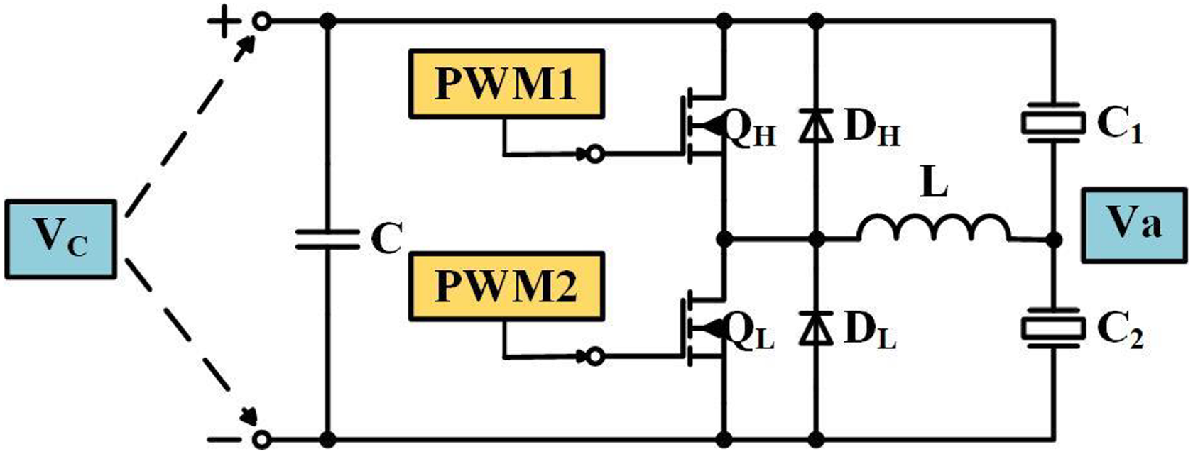
Circuit of DC/AC stage.
In this design, energy transition can be described in two parts. The first part is in the DC/DC stage, that is, the flyback topology in DCM. When the switch is turned on, the energy is stored in the capacitor by primary and secondary inductances through diode D; when the switch is turned off, the energy is provided to the load while consuming energy in the capacitor. The second part is in the DC/AC stage. The waveform cycle used to generate two square signals, which is utilized to illustrate the energy transition, can be divided into six steps, as shown in Figure 6.
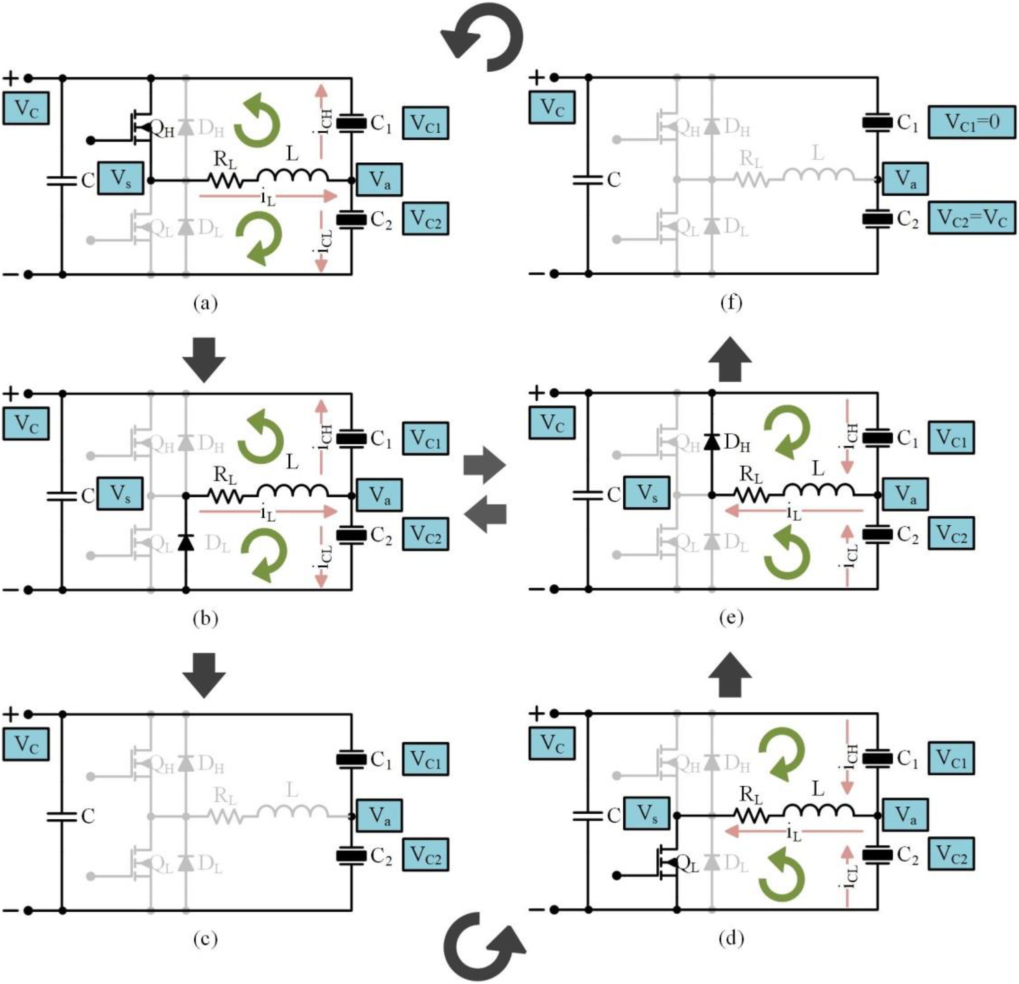
Energy transition in the high-voltage driving circuit, including six modes (a) to (f) in a cycle.
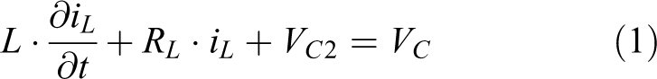
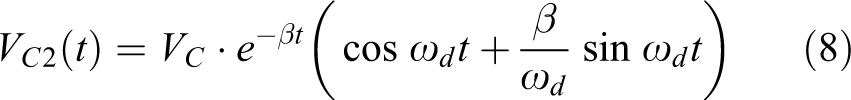
In mode (a), inductor current iL increases when switch QH is turned on. The unused energy in the actuator at the upper side is transferred to the actuator at the lower side. According to Kirchhoff’s voltage law

As a result, the calculated formula can be expressed as

In an underdamped oscillation condition
The parameters used above are shown in Table 1.
Parameters used in the formulas.

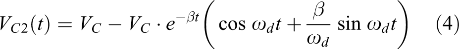
The theoretical calculation indicates that driving signal voltage VC 2(t) increases to near VC .
In mode (b), inductor current iL decreases and flows through freewheeling diode D when QH is turned off.


As a result, the calculated formula can be expressed as

Driving signal voltage VC 2(t) decreases while the energy stored in inductor L is exhausted.
In mode (c), the actuator at the lower side is fully charged, whereas the actuator at the upper side and inductor L are empty. During this period, driving signal voltage VC 2 is similar to VC . The entire unused energy is transferred from the actuator at the upper side to the actuator at the lower side.
In mode (d), inductor current iL increases in reverse when switch QL is turned on. The unused energy in the actuator at the lower side is transferred to inductor L
In mode (e), inductor current iL decreases and flows through freewheeling diode D when switch QL is turned off. Energy is transferred to the actuator at the upper side

In mode (f), driving signal voltage VC 1(t) is charged to VC while unused energy is completely transferred from the actuator at the lower side to the actuator at the upper side.
In the cycle shown in Figure 7, two driving signals with a phase difference of 180° can be generated to drive the piezoelectric actuator by controlling the charge and discharge periods. The unused energy in the capacitive piezoelectric actuator is utilized to achieve high conversion efficiency, and the overall efficiency of the system is enhanced effectively.

Waveforms in an energy transition cycle.
Experimental results
Converter prototype
On the basis of the theory mentioned in “Design and analysis of the driving circuit” section, a micro driving circuit shown in Figure 8 was fabricated with surface mount discrete components soldered on a well-designed printed circuit broad (PCB) that includes DC/DC and DC/AC stages. The length, width, and thickness of the circuit are 14, 12, and 4 mm, respectively.

Display of the micro driving circuit.
The components of the micro converter are shown in Table 2. The total mass of the circuit is 91 mg. The components of the circuit, including MOS transistors, diodes, and coupled inductors, were considered. According to the 102 mA level input and 101 mA level output in the DC/DC stage and based on the package specifications, N-channel enhancement-mode MOSFET Si2304DS with SOT-23 package, 30 V drain-source voltage, and 2.5 A continuous drain current was used. In the DC/AC stage, with the same package and characteristics, 240 V drain-source voltage MOSFET TK2404K was utilized because of its high output voltage. For the diode beside the secondary inductance, Schottky barrier rectifier diode SMD1200PL with SOD-123 package, 1 A average forward current, and 200 V maximum recurrent peak reverse voltage was selected. Compared with the 0.7 V forward voltage of a conventional diode, the value of the Schottky barrier is 0.4 V, which means lower conduction losses. The mini-sized coupled inductor LPR4012-202LMRC with an excellent coupling coefficient (k = 0.95) has 2 µH primary inductance, 1:10 turn ratio, 1.70 A Isat, and L1 0.240 Ohms and L2 11.62 Ohms DC resistance (DCR). High and low DCR ratings of these low profile parts provide high efficiency and excellent current handling in a rugged, low-cost design.
Converter components.

Additionally, Bare-die saves space on PCB and can be wire-bonded directly on the top of the circuit substrate. By comparison, chip-scale components are more robust in terms of strong mechanical support, high electrical conduction, and high thermal conduction. As a prototype, this circuit can be improved by bare-die components and lithium batteries, supercapacitors, 31 solar cells, 32 as well as fuel cells 33 for further miniaturization and feasibility, which has the potential to be applied in sub-centimeter scale robots in the future.
In the DC/DC stage, the node waveforms of VGS , VDS , and iL1 were obtained, as shown in Figure 9. The waveforms are consistent with the theoretical analysis. The zero current shows that the circuit worked in flyback DCM.

Node waveforms of the flyback circuit.
In the DC/DC stage, a DC voltage of up to 100 V was obtained from a 3.7 V lithium battery. The voltages of each node (i.e. Vbat , VL , VH , and VC ) in (a) sinusoidal, (b) square, and (c) triangle driving modes are shown in Figure 10. The oscilloscope probe was used five times to measure 100 V voltage.

Voltages of the DC/AC stage in (a) sinusoidal, (b) square, and (c) triangle driving modes.
Conversion efficiency is related to various drive voltages and output powers in the converter. The dominant loss is from transistors and copper windings.
At a constant load condition and the related constant power output, conduction losses are dominant at low drive voltages because of the large currents. In small currents with high driving voltages, the conduction losses decrease, which in turn increases efficiency. However, when the driving voltage increases to above a certain value, the losses from iron become dominant due to the large current swing caused by the large duty cycle of PWM, which reduces efficiency.
Figure 11 shows that the peak power efficiency of the converter is 84.6% at around 0.28 W output power under 100 V AC voltage, and this value is an acceptable transferred efficiency.

Power efficiency under output voltages of 80, 100, and 120 V.
Piezoelectric bimorph used for testing
The piezoelectric bimorph (PANT, QDTE52-7.0-0.82-4) used for testing has the parameters of 0 to 190 V driving voltage, 52 × 7.0 × 0.82 mm size, 1.2 mm bidirectional displacement, and 50 Hz resonant frequency. The resonant frequency of the piezoelectric bimorph 80 Hz is close to the driving frequency of an insect-type flying robot. Therefore, the actuator can acquire large displacement.
Figure 12 presents an image of the entire system comprising a battery box, the proposed interface, and a manual probe station used in conjunction with the I/V Power Device Analyzer (AGILENT, B1505A).
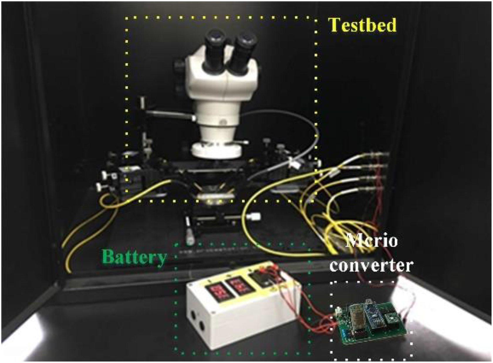
Display of entire system.
Figure 13(a) to (c) shows the deformation of the front end of piezoelectric actuator under voltages of 0, 50, and 100V, respectively. All of images are taken from the same view of the microscope. It can be seen from the figure that as the voltage applied to the actuator increases, the degree of deformation also increases, which eventually resulting in a displacement of about 0.5 mm in the case of unidirectional deformation.
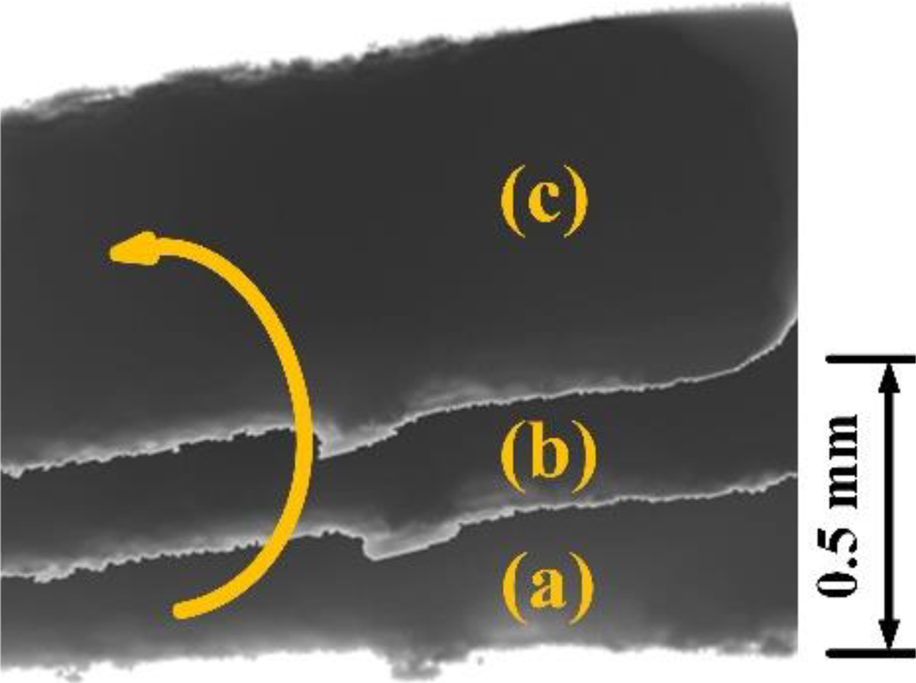
The deformation at the front end of the actuator under different voltages of (a) 0 V, (b) 50 V, and (c) 100 V.
Figure 14 is an image of the actuator in three statuses of (a) equilibrium, (b) up, and (c) down under voltages of 0, 100, −100 V, respectively, in the case of deformation in both directions. The displacement of up-down movement is approaching 1 mm, which could be further enlarged with a mechanically magnified structure to obtain a potential ability to be applied in mobile robot.

The deformation at the front end in a cycle, where, (a) equilibrium, (b) up, and (c) down, under voltages of 0 V, 100 V, and −100 V, respectively.
Conclusion
In this study, a micro converter for a piezoelectric bimorph was designed and implemented. This micro converter has the potential to be applied in micro mobile robots because of its advantages of high efficiency at low power and micro size. The contributions of this study are the design and implementation of a circuit topology supplying power for micro mobile robots at low power, realization of its miniaturization, and explanation of the energy transition through a relevant analysis of the circuit, which is the reason for the high efficiency. Combined with mechanical structures, it can be applied to some robots to achieve telescopic, traveling, and other unidirectional control operations. 34,35 Our next work will include further reduction in circuit losses to improve efficiency and a chip-based design to reduce size and mass, with further development in the miniaturization of the electronic component.
Footnotes
Declaration of conflicting interests
The author(s) declares no potential conflicts of interest with respect to the research, authorship, and/or publication of this article.
Funding
The author(s) disclosed receipt of the following financial support for the research, authorship, and/or publication of this article: This research was supported by the National Natural Science Foundation of China (No. 61403160), China Postdoctoral Science Foundation (Nos. 2016T90259, 2014M551194), and Science and Technology Office, Jilin Province of China (No. 20150414052GH).