
Abstract
The nano-metric cutting process of single-crystal SiO2 was studied using molecular dynamics simulation, where the effects of anisotropy on material removal and surface integrity were analyzed. The typical crystal directions on different crystal planes of SiO2 were selected as cutting directions. The results show that the chip formation, temperature distribution in the machined area, cutting force, phase transformation and damage layer thickness vary according to the cutting direction. The crystal orientation of (110) [00−1] exhibits a large range of damage expansion while (110) [1−10] exhibits the smallest range. In addition, the radial distribution function results show that SiO2 workpieces cut in different directions vary in crystal phase type and content to some degree, while a new phase is produced in the cutting direction of (111) [−101]. Therefore, the anisotropy of the selection of crystal planes and crystal directions is of great significance for the nano-metric cutting of SiO2 to obtain quality machined surfaces of SiO2.
Introduction
Nanomachining is an essential processing technology used for obtaining quality machined surfaces with high precision.1–5 The dimensional accuracy and surface integrity that nanotechnology can achieve has become a yardstick by which the level of a country’s manufacturing industry is measured. As a frontier in the field of micro-nano machining, nano-metric cutting of SiO2 in ductile mode using a diamond tool has attracted increasing attention. Nowadays, SiO2 crystals are widely used in varied fields such as computers, electronic information, and aerospace. More importantly, SiO2 is a common material in the high-power multi-pass laser amplifier system.6,7 In this application, to achieve a successful inertial confinement fusion ignition and increase the light throughput and service life of the system, it is crucial to ensure the surface integrity and machining precision of SiO2.
Presently, the molecular dynamics (MD) method is widely used for research on the nano-metric machining process and material removal mechanism,8–11 whereby many research results have been obtained. In 1990, Hoover et al. studied a large-scale elastoplastic indentation simulation based on non-equilibrium MD, representing the first time that MD had been applied to ultra-precision machining research. 12 In 1995, the Japanese scholars Shimada et al. adopted MD for studying the nano-cutting mechanism from the perspectives of the deformation, micromorphology and lattice deformation energy of the material. They reported that MD was a very effective tool for studying the micro/nano-cutting process.13,14 Komanduri et al. studied the nano-cutting of single-crystal aluminum where, via analysis of the dislocation expansion in the machining process, they found the extent of anisotropy in single-crystal aluminum. 15
According to the results of previous studies, the cutting direction has a great effect on the surface topography and machining accuracy of a crystalline workpiece.16,17 Further, with the development of computer technology, the MD method has gradually been applied to research of the nano-metric cutting process for medium and low cutting speeds. Ye et al. studied the nano-metric cutting process of single-crystal copper, and discussed the effects of different cutting speeds on the material removal mechanism. 18 Tanaka et al. studied the ductile cutting of monocrystalline silicon using deformation analysis, studying the influence of the cutting depth, edge radius and tool angle on the force distribution. In addition, this previous report discussed the mechanisms of crystal-phase transformation and amorphous phase transformation during the cutting process of single-crystal silicon. 19 Saha et al. studied the influence of nanowire grain size, temperature and diameter on the deformation and plasticity of polycrystalline tungsten nanowires. It was then found that an inverse Hall-Petch effect would occur when the grain size was less than the critical value of 14.91 nm. 20 Liang et al. studied the mechanical strength and coordination defects of compressed quartz glass, drawing the conclusion that the decrease of mechanical strength and the permanent densification were caused by coordination defects. 21 With the improvement of MD simulation technology, nanomachining models have been well developed, and many remarkable achievements have been made by combining MD simulations with experiments.22–25
As mentioned, MD has been widely applied to research on monocrystalline materials such as single-crystal copper, 26 aluminum,26,27 silicon 25 and germanium. 28 However, fewer reports exist on the nano-cutting of polycrystalline and amorphous materials. When it comes to polycrystalline materials, much attention has been paid to the mechanical properties of rare metals such as tungsten, molybdenum and nickel,20,29,30 which are used to manufacture nanowires. As for the amorphous materials, many scholars have carried out extensive research on amorphous SiO2, such as fused quartz and silica glass,31–35 in the aspects of mechanical properties and nano-metric machining mechanisms. Nevertheless, the research on single-crystal SiO2 is insufficient, and especially with regard to the influence of anisotropy on the nano-metric cutting behavior of single-crystal SiO2.
In this paper, a three-dimensional simulation model for cutting single-crystal SiO2 in ductile mode is established based on the theoretical knowledge of MD and nanomachining. Further, this paper studies the influence of anisotropy on the cutting process and surface integrity of single-crystal SiO2 for various cutting directions. This work will give information for effective parameter optimization to obtain quality machined surfaces of SiO2 with high precision.
Modeling and Methods
The LAMMPS Molecular Dynamics Simulator36,37 was applied to model an SiO2 workpiece as cut by a diamond tool. The workpiece size was set to be 265 Å×145 Å×165 Å with the total number of atoms being 510282. The workpiece was divided into three layers including the Newton layer, thermostatic layer and boundary layer. In the Newton layer, all atoms follow Newtonian laws of motion; the thermostatic layer is used to simulate the heat dissipation during the actual cutting; while the boundary layer is equivalent to a fixture used to fix the workpiece. Next, the thickness of the boundary layer and thermostatic layer was set to be 1 and 2 nm respectively. The thermostatic layer was chosen to be 1 nm thicker than the boundary layer so that the temperature could be well controlled, even with such a large workpiece size. Because the hardness of the SiO2 crystal (i.e., Moh’s hardness of 7) is much lower than that of the diamond tool (i.e., Moh’s hardness of 10), the diamond tool could be simplified as a rigid body to improve the computational efficiency. Finally, the cutting-edge radius was 25 Å; the rake and clearance angles were −7° and 7°, respectively; and the tool size was 84 Å×39 Å×96 Å with the total number of carbon atoms being 50844. Figure 1 shows the simulation model built herein.

Nano-metric cutting model of SiO2.
After establishing the nano-metric cutting model of SiO2, the machining parameters were initialized. A simulation time step of 1 fs was selected after an overall consideration of the computational accuracy and computational efficiency. The simulation adopted a fixed boundary condition in the X and Z directions and a periodic boundary condition in the Y direction. In the periodic boundary condition, when an atom leaves a simulation box in one direction along the Y axis, it will enter the simulation box from the other direction at the same speed. This ensures that the number of the particles in the system is constant and the boundary effect is eliminated based on the minimum-image convention. In addition, this study selected the micro-canonical ensemble (NVE), wherein the system’s total number of particles, total volume and total energy were constant during the simulation. In the NVE ensemble, a system with N particles whose coordinate vector is

where M is the mass of particles, t is time and a dotted vector signifies a derivative with respect to time. The potential function U(

where r is the distance between the interacting atoms, re is the equilibrium bond distance, D is the potential well depth, and a controls the “width” of the well, where a smaller a creates a larger well. The rest of the atomic interactions, such as C–C, Si–Si, and O–O, are described by the Tersoff potential function, as given as

where Ei is the site energy of the ith atom; Vij and rij are respectively the bonding energy and bond length between the ith and jth atoms ; fC is a truncation function; fR and fA reflect the repulsive and attractive interactions, respectively; and bij is a modulation function related to the bond angle and the relative position between particles i and j.
To simplify the calculation, the bonding interaction Ebond is ignored . Thus, only the nonbonding interaction Enonbond is taken into account, namely, the van der Waals’ force and Coulomb force. These nonbonding forces are separately described by the Lennard-Jones (12-6) pair potential and the electrostatic force. Parameters for the nonbonding interaction are given in Table 1, and the potential energy for the total interaction Etotal and the nonbonding interaction Enonbond can be calculated using Eqs. (4)–(5), respectively. Though the bonding interaction Ebond is a portion of the Etotal of Eq. (4), it is not calculated here because the Ebond interaction is ignored, as mentioned earlier.


Parameters for the nonbonding interaction, including atom type, van der Waals radius (σ), well depth (E), and the atom charge (q).

where σij is the molecular diameter (distance of closest approach) between the ith and jth atoms; εij is the depth of the potential well produced between the ith and jth atoms; qi and qj are the charge of the ith and jth atom, respectively; and ε0 is the permittivity of free space .
Results and discussion
Nano-cutting process of single-crystal SiO2
Herein, the nano-metric cutting process of monocrystalline SiO2 was analyzed at a cutting depth of 10 Å and a cutting speed of 200 m/s. Figure 2 shows the temperature distribution in the workpiece and chips at different cutting distances during the cutting process. It can be seen that chips accumulate in front of the tool but not at the back of the tool. In addition, the chip accumulation follows a certain rule. Namely, as machining proceeds, the chips continuously pile up and into an increasingly larger heap. When the heap height reaches a certain value, the chip heap falls apart owing to the vibration of the cutting tool. This piling up and peeling off of the chip heap is a repeated process during machining. Different cutting parameters will induce a shorter or longer piling up-peeling off cycle, but this process is consistent on the whole.

Temperature distribution in workpiece and chips with cutting depth of 2 Å at a cutting distance of (a) 119 Å; (b) 134 Å; (c) 149 Å; (d) 164 Å; (e) 179 Å; (f) 194 Å. Cutting speed is 200 m/s.
Figure 3 shows the evolution of chip formation during the cutting process after increasing the cutting depth. It can be seen that the stock removal increases when the cutting depth is increased to 20 Å. As a result, more chips accumulate on the un-machined surface, and thus the piling up-peeling off cycle of the chips is shortened. In addition, when the workpiece is cut at a large cutting depth, the chip is greatly influenced by the vibration of the tool. Therefore, the discontinuity of chips is more significant and the chip side-flow occurs easily. This causes some chips to pile up on the machined surface and thereby affect the surface integrity.
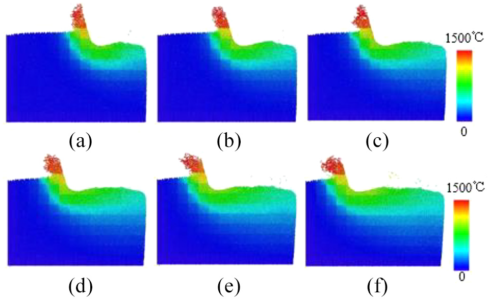
Temperature distribution in workpiece and chips with cutting depth of 20 Å at a cutting distance of (a) 119 Å; (b) 134 Å; (c) 149 Å; (d) 164 Å; (e) 179 Å; (f) 194 Å. Cutting speed is 200 m/s.
Comparing Figures 2 and 3, it can be seen that the depth of the zone influenced by temperature is several times greater than the cutting depth. Moreover, increasing the cutting depth induces a more significant rebound phenomenon, or spring-back, of the machined surface. For ultra-precision machining, the cutting depth is at the nano-metric scale, which is much smaller than the average grain size (17). Hence, the spring-back cannot be ignored. With increased cutting depth, the extrusion effect of the tool on the workpiece is enhanced. If the extrusion effect makes the strain energy of the workpiece greater than the critical value, the extruded atoms of the workpiece are reorganized. If the energy required for reorganization is not fully provided by extrusion, however, then intergranular dislocation occurs. During the cutting process, the diamond tool moves forward until the extrusion effect on the machined surface disappears. After that, one of two scenarios will occur. On the one hand, the atoms that move slightly but have not re-bonded under extrusion will return to their original position, resulting in an elastic recovery (i.e., spring-back) of the machined surface. Specifically, greater cutting depths create a more significant spring-back. On the other hand, atoms that form new covalent bonds in the reorganization process under extrusion will not return to their original position, resulting in plastic deformation.
It is also found that the temperature of the chip is very high during the cutting process. This will lead to phase transformation, thus changing the micro-topography of the workpiece surface to a certain extent. Moreover, the chip temperature initially decreases and then increases, which is related to the process of chips piling up and peeling off. That is, the accumulation of chips increases the working rake angle of the diamond tool, which is beneficial for reducing the deformation and thus decreasing the cutting heat. As the chips subsequently peel off, the cutting temperature increases because the working rake angle decreases.
Influence of anisotropy on the nano-metric cutting of single-crystal SiO2
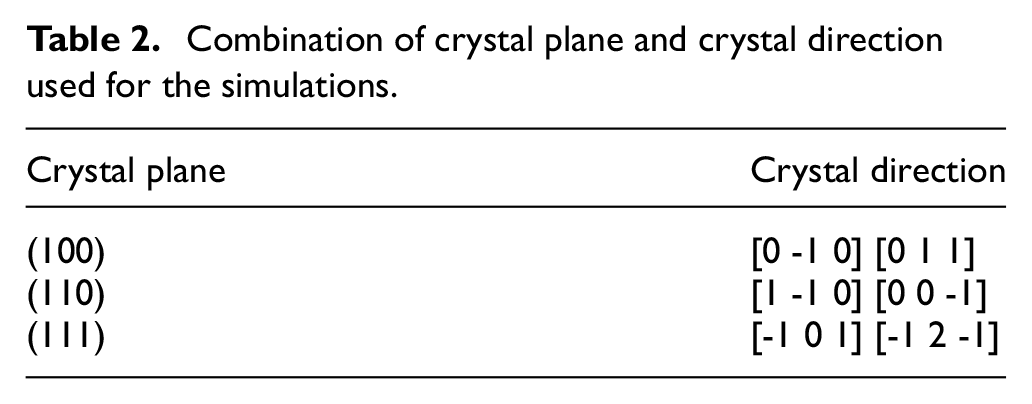
The physical and mechanical properties of crystal materials have obvious anisotropy in different crystal planes and crystal directions. Hitherto, the (100), (110), and (111) crystal planes have been extensively studied in many experiments and simulations. In this paper, we constructed six simulation models where the SiO2 workpiece was cut on the (100), (110), and (111) crystal planes in two crystal directions for each crystal plane, as shown in Table 2. The cutting speed was set as 200 m/s with a cutting depth of 10 Å.
Combination of crystal plane and crystal direction used for the simulations.
Influence of cutting directions on temperature
First, we analyzed the temperature distribution in the workpiece for various cutting directions and at a cutting distance of 130 Å, as shown in Figure 4.

Temperature distribution on the X-Z plane at a cutting distance of 130 Å for a cutting direction of (a) (100)[0 −1 0]; (b) (100)[0 1 1]; (c) (110)[1 −1 0]; (d) (110)[0 0 −1]; (e) (111)[−1 0 1]; (f) (111)[ −1 2 −1].
As can be seen from Figure 4, of the six scenarios, the workpieces cut in the (110) [1−10], (100) [0−10] and (111) [−101] directions exhibit the more obvious chip formation. Of these, the chip formation in the cutting direction of (110) [1−10] is the most obvious. This variation of chip formation is because the intensity of the atomic arrangement varies with the crystal orientation of the workpiece. The atoms of the workpiece are the most densely arranged in the (110) [1−10] direction, and thus the greatest chip generation occurs when the workpiece is cut in this direction. By contrast, atoms of the workpiece are the most sparsely arranged in the (111) [−12−1] direction, so only traces of plowing occur. In this latter case, the workpiece is deformed but no material is removed. Instead, the workpiece atoms are plowed by the tool and then pushed to both sides, which is not ideal. To improve the machining efficiency, therefore, the material removal rate should be increased on the premise of achieving the specified machining accuracy. It is also found that, when cut in the (100) [011] and (110) [1−10] directions, the workpiece exhibits less spring-back than when cut in the other four crystal directions. This signifies that, for workpieces cut in the (100) [011] and (110) [1−10] directions, the generated strain is sufficient to break and then reorganize most of the covalent bonds of the workpiece atoms. This is beneficial for ductile cutting and thus the machining precision is improved. According to the radial distribution function, as shown in Figure 8(c), when the workpiece is cut in the (110) [1−10] crystal direction, the reorganization process increases the content of the phase with an Si–O bond length of 1.59 Å.
Next, the temperature distribution was analyzed according to the vertical view, as shown in Figure 5.

Temperature distribution on the X-Y plane according to the vertical view for a cutting direction of (a) (100)[0 −1 0]; (b) (100)[0 1 1]; (c) (110)[1 −1 0]; (d) (110)[0 0 −1]; (e) (111)[ −1 0 1]; (f) (111)[−1 2 −1].
Figure 4 shows that the (110) [00−1] cutting direction leads to the widest temperature diffusion range in the Z direction, while the (110) [1−10] cutting direction causes the smallest Z-direction temperature influence. As can be seen from Figure 5, the (100) [0−10] and (111) [−101] cutting directions cause the workpiece to be greatly affected by the temperature in the Y direction, and the temperature gradient is large. The subsequent inhomogeneous heat will generate thermal stress, which can easily induce internal defects such as micro-cracks. As for the (100) [011] and (111) [−12−1] cutting directions, although they cause a large temperature diffusion range in the Y direction, the cutting temperature is low and the distribution is more homogeneous. This is beneficial for an improved processing quality. As an ideal, the workpiece cut in the (110) [1−10] direction, exhibits a low temperature and a small range of temperature diffusion in the workpiece.
Influence of cutting direction on the cutting force
Cutting force is an important factor for measuring machining stability and accuracy. The cutting force at a cutting speed of 200 m/s and a cutting depth of 10 Å for different cutting directions is analyzed, as shown in Figure 6.

Cutting force at a cutting speed of 200 m/s and a cutting depth of 10 Å for various cutting directions.
As shown in Figure 6, when an SiO2 crystal is cut in the directions of (111) [−101], (110) [1−10], and (100) [0−10], the cutting forces are relatively large and their fluctuations are evident. By contrast, the cutting forces and their fluctuations produced in the other three cutting directions are much smaller. A large cutting force fluctuation indicates that many atomic covalent bonds are breaking and re-bonding. In addition, during the cutting process, the interaction of tool atoms with workpiece atoms is at a maximum after the tool cuts into the workpiece completely. This explains the gradual increase of the cutting forces to a peak value. After reaching the peak value, the cutting forces for the (111) [−101], (110) [1−10] and (100) [0−10] cutting directions begin to drop. This is because the increase of the cutting force causes the temperature of the workpiece to rise. When the temperature is greater than a critical value, the thermal soft effect initiated in the workpiece increases the interatomic distance. This subsequently weakens the bonding forces between atoms, and thus the cutting force is reduced until it reaches a balanced state (i.e., stable stage). Figure 7 shows the average cutting forces generated in different cutting directions at the stable stage.
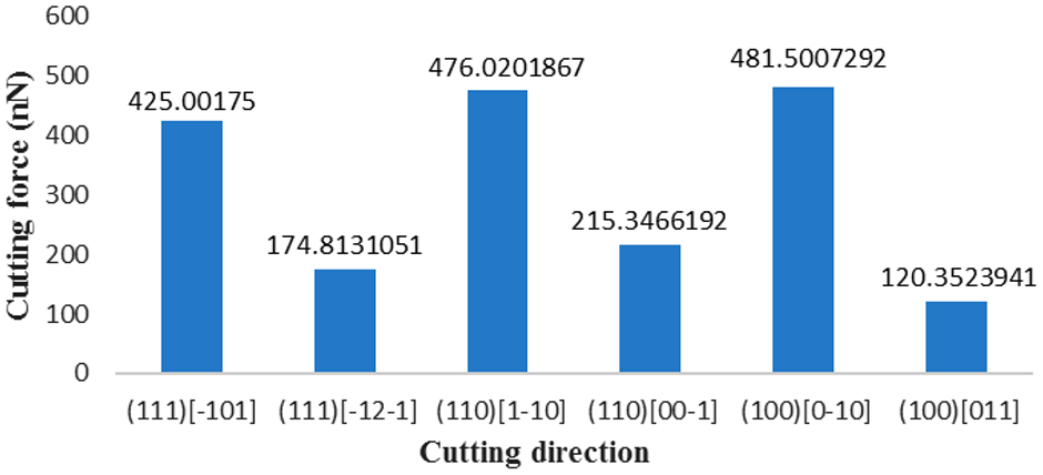
Average cutting forces generated in different cutting directions at the stable stage.
The average cutting force for the (100) [0−10] cutting direction (481 nN) is the greatest, while the smallest average cutting force is generated in the (100) [011] cutting direction (120 nN). Therefore, the average cutting force as a function of anisotropy varies by about 75%, which fully illustrates that the proper selection of cutting direction is very important.
Influence of cutting direction on the type and content of formed phases
Next, the radial distribution function (RDF) of the system was used to analyze the structure and composition of the particle system. The RDF of the initial and final states for each cutting direction was analyzed for a cut-off radius set at 2.5 Å, and the result is shown in Figure 8.

Radial distribution function (RDF) of the system, used to analyze the structure and composition of the particle system. The cut-off radius is set at 2.5 Å, and the RDF of the initial and final states for different cutting directions is analyzed. The cutting directions studied include (a) (100)[0 −1 0]; (b) (100)[0 1 1]; (c) (110)[1 −1 0]; (d) (110)[0 0 −1]; (e) (111)[−1 0 1]; (f) (111)[−1 2 −1].
Figure 8 shows a slight variation in the location and value of the peaks for each crystal orientation. This indicates that the workpieces vary in the type and content of phases according to the crystal direction along which the workpiece is generated. When the workpieces are generated along different crystal orientations, the arrangement and bonding of their atoms will differ. This leads to distinct physical and chemical properties of the workpiece in each crystal direction. Compared with the (100) [0−10], (110)[1−10] and (111)[ −101] crystal directions, the RDF curves of the (100)[011], (110)[00−1] and (111)[ −12−1] crystal directions have sharp peaks before processing. This shows that the workpieces generated along the (100) [011], (110) [00−1] and (111) [−12−1] crystal orientations have a strong ability to maintain the original atomic aggregation state after relaxation; namely, their structures are more stable. Moreover, for the (111) [−101] cutting direction at a cutting speed of 200 m/s and a cutting depth of 10 Å, the initial phase with a bond length of 1.6425 Å is reorganized into a new phase with a bond length of 1.6525 Å after processing. For the other cutting directions, however, only the phase content changes after processing. Among them, the (100) [0−10] and (110) [1−10] cutting directions exhibit primary phases of α-quartz with an Si–O bond length of 1.59 Å and β-quartz with an Si–O bond length of 1.62 Å, both before and after processing. In the other three cutting directions of (100) [011], (110) [00−1] and (111) [−12−1], however, there exist more crystal phase types. Specifically, the crystal orientation of (100) [011] also exhibits phases with bond lengths of 1.59 and 1.62 Å, as well as phases with bond lengths of 1.33, 1.5, 2.31, 2.39 and 2.41 Å. The crystal orientation of (110) [00−1] exhibits some phases with bond lengths of 1.81 and 1.85 Å, which may be some forms of the Si–Si or Si–O bonds. Also, the peaks of the RDF curves after processing are no longer as sharp as they were before, indicating that the atomic arrangements tend to be disordered after processing and many amorphous phases are generated in the workpieces.
Analysis of coordination number
The coordination number, referring to the number of atoms bonded to the center atom, can be used to study the phase transformation during the cutting process. We therefore analyzed the coordination number distribution for the different cutting directions at a cutting speed of 200 m/s, a cutting depth of 10 Å, and a cutting distance of 133 Å. The results are shown in Figure 9.

Coordination number distribution at a cutting speed of 200 m/s, a cutting depth of 10 Å, and a cutting distance of 133 Å for a cutting direction of (a) (100)[0 −1 0]; (b) (100)[0 1 1]; (c) (110)[1 −1 0]; (d) (110)[0 0 −1]; (e) (111)[ −1 0 1]; (f) (111)[ −1 2 −1].
The atomic densification region constitutes the damage layer structure of the workpiece. Under the extrusion of the machining tool, the four-fold coordinated silicon atoms are further bonded with additional oxygen atoms to become five- or six-fold coordinated silicon atoms. This increases the local density and forms a new irregular microstructure. Ideally, the cutting direction that generates a damage layer with a small thickness should be selected. As shown in Figure 9, the (110) [00−1] cutting direction exhibits a wide distribution of atoms with coordination numbers of 5 and 6, indicating a large range of damage expansion. Therefore, the (110) [00−1] cutting direction should be avoided. By contrast, the thickness of the damage layer is relatively small for the crystal orientations of (100) [0−10], (110) [1−10] and (111) [−101], and is the smallest for the (110) [1−10] direction.
Conclusions
In this paper, the nano-metric cutting process of single-crystal SiO2 is studied from an atomic perspective. The relationship between chip formation and temperature change in the chip is discussed first. Then this paper explores the influence of anisotropy on the temperature distribution, the cutting force, the change of phase type and content, and the damage layer in the cutting process. The following conclusions are drawn:
During cutting, the chips constantly pile up in front of the diamond tool and subsequently peel off. The chip temperature changes according to the cycle of chip formation and removal. Moreover, the intensity of atomic arrangement affects the chip formation. Chip generation is the most obvious in the (110) [1−10] direction, while only the plowing effect takes place in the (111) [−12−1] direction.
The temperature distribution in the workpiece varies with cutting directions. The (100) [0−10] and (111) [−101] directions exhibit a wide temperature diffusion range in the Y direction with a large temperature gradient, which is likely to cause internal defects such as micro-cracks. The (100) [011] and (111) [−12−1] cutting directions exhibit a low temperature that is evenly distributed, which is beneficial for improving the machining quality. It is worth noting that, for the (110) [1−10] cutting direction, the temperature is low and its diffusion range is small.
Cutting along the various crystal orientations has a significant effect on the cutting force as well as the damage layer thickness. The (111) [−101], (110) [1−10] and (100) [0−10] cutting directions exhibit a large cutting force that has obvious fluctuation, which is detrimental to ductile cutting. In addition, the (110) [1−10] cutting direction exhibits the thinnest generated damage layer. However, for the (110) [00−1] cutting direction, the widespread occurrence of five- and six-fold atoms indicates serious damage.
The crystal orientation has a significant effect on the type and content of the phases formed during the cutting process. The (111) [−101] cutting direction exhibits an initial phase with a bond length of 1.6425 Å that is reorganized into a new phase with a bond length of 1.6525 Å after processing.
In short, based on factors such as temperature distribution, cutting force, chip formation and damage layer thickness, the crystal directions for each crystal plane most suitable for ductile cutting are (100) [0−10], (110) [1−10] and (111) [−101], with the (110) [1−10] direction being the best and (110) [00−1] the worst.
Footnotes
Handling Editor: James Baldwin
Author Contributions
Conceptualization, J.C., F.W., and L.L.; methodology, M.L. and J.Q.; formal analysis, M.L., X.M., and L.N.; investigation, H.L., M.L., G.Z., and X.Y.; writing—original draft preparation, M.L., H.P. and Q.S.; funding acquisition, J.C.
Declaration of Conflicting Interests
The author(s) declared no potential conflicts of interest with respect to the research, authorship, and/or publication of this article.
Funding
The author(s) disclosed receipt of the following financial support for the research, authorship, and/or publication of this article: This work was supplied by the Key Natural Science Foundation (51535003), Natural Science Foundation (51505331), the Natural Science Foundation of Heilongjiang Province in China (E2015007), the Harbin Innovative Talents Fund (RC2013XK006010), the Harbin Outstanding Youth Science Fund (2015RAYGJ002), the Fundamental Research, the Postdoctoral Scientific Research Developmental Fund (LBH-Q16111), and the Funds for the Central Universities (Grant No. HIT.NSRIF.2012036).