
Abstract
We present a resonant magnetic field sensor based on microelectromechanical systems technology with optical detection. The sensor has single resonator composed of two orthogonal silicon beams (600 µm × 26 µm × 2 µm) with an integrated mirror (50 µm × 34 µm × 0.11 µm) and gold tracks (16 µm × 0.11 µm). The resonator is fabricated using silicon-on-insulator wafer in a simple bulk micromachining process. The sensor has easy performance that allows its oscillation in the first bending vibration mode through the Lorentz force for monitoring in-plane magnetic field. Analytical models are developed to predict first bending resonant frequency, quality factor, and displacements of the resonator. In addition, finite element method models are obtained to estimate the resonator performance. The results of the proposed analytical models agree well with those of the finite element method models. For alternating electrical current of 30 mA, the sensor has a theoretical linear response, a first bending resonant frequency of 43.8 kHz, a sensitivity of 46.1 µm T−1, and a power consumption close to 54 mW. The experimental resonant frequency of the sensor is 53 kHz. The proposed sensor could be used for monitoring in-plane magnetic field without a complex signal conditioning system.
Keywords
Introduction
Silicon micromachined resonators have been used in magnetic field sensors due to their advantages such as small size, low power consumption, adjustable dynamic range and high sensitivity.1,2 These sensors have potential applications such as telecommunications, navigation, aerospace, consumer electronics products, and biomedicine.3–6 Generally, they operate using the principle of Lorentz force or electromagnetic induction.7–11 The sensors based on electromagnetic induction will detect external magnetic field through electromotive force in an induction coil. On the other hand, sensors that operate with Lorentz force can detect magnetic field through displacements of their resonators, which are related with the magnitude and direction of the applied magnetic field.
Recently, some research groups have developed magnetic field sensors considering silicon resonators.7–21 These sensors are smaller than the conventional superconducting quantum interference devices, fluxgate sensors, and optical fiber sensors. Silicon resonators-based sensors can be fabricated using batch standard silicon micromachined fabrication processes, which decrease their cost and allow the integration with electronic circuits. These sensors can be located closer of magnetic field sources for increasing their output signals. In addition, the dynamic range of these sensors is adjusted modifying the Lorentz force through the variation of the excitation electrical current. Also, these sensors can employ different sensing techniques, including the piezoresistive, capacitive, optical, or piezoelectric.12–21 For instance, sensors with piezoresistive transduction have a simple operation principle and easy signal conditioning, but commonly they present offset voltages and their performance may be altered by temperature shifts. Instead, the magnetic field sensors with capacitive detection have less temperature dependence than those with piezoresistive sensing. However, capacitive sensors present parasitic capacitances and need vacuum packaging to decrease the viscous damping. Generally, magnetic field sensors with piezoelectric transduction require piezoelectric layers deposited on silicon resonators, which increase the stages of their fabrication processes. On the other hand, optical readout systems permit the reduction of electronic circuits in magnetic field sensors as well as immunity to electromagnetic interference (EMI). Most of the magnetic field sensors only detect a normal component of magnetic field, restricting their application range. Other sensors14,15,17 need to oscillate in different vibration modes to detect two or three normal components of magnetic field. To overcome this problem, we develop a resonant microelectromechanical systems (MEMS) magnetic field sensor composed of two orthogonal silicon beams with integrated mirror that are fabricated using a non-complex bulk micromachining process. This sensor only requires to oscillate at its first bending vibration mode using Lorentz force for monitoring in-plane magnetic field. The sensor has an easy performance with optical detection that allows to decrease its electronic circuits. The proposed sensor has linear response, small size, safe mechanical behavior, low power consumption, and simple signal conditioning. This sensor could be employed in some electronic consumer products due to its small size, easy performance, and wide dynamic range.
This article is organized as follows: section “Design and modeling” describes the mechanical design and modeling of magnetic field sensor. Section “Fabrication” includes the sensor fabrication using a bulk micromachining process. Section “Results and discussion” shows the results and discussions about the mechanical behavior of magnetic field sensor. Finally, section “Conclusion” reports the conclusions and future researches.
Design and modeling
In this section, we present the design and analytical modeling of the performance of an in-plane magnetic field sensor based on silicon resonator.
Electrical and mechanical configuration
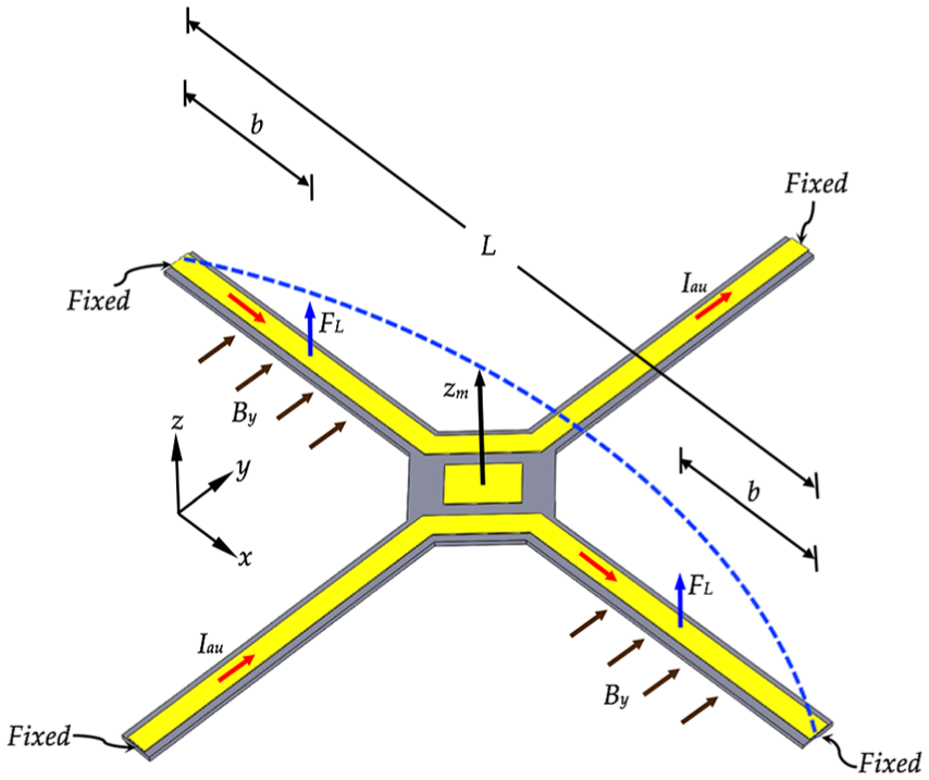
The magnetic field sensor has a silicon resonator composed of two orthogonal beams (600 µm × 26 µm × 2 µm), two gold tracks (16 µm × 0.11 µm), and a gold mirror (50 µm × 34 µm × 0.11 µm), as shown in Figure 1. The two tracks are supplied with sinusoidal excitation currents under a frequency equal to the first bending resonant frequency of the resonator. Hence, Lorentz forces are generated when the excitation current interacts with in-plane magnetic field, causing out-of-plane displacements of the mirror that are related with the applied magnetic field. The displacements are increased when the structure operates at its first bending resonant frequency.
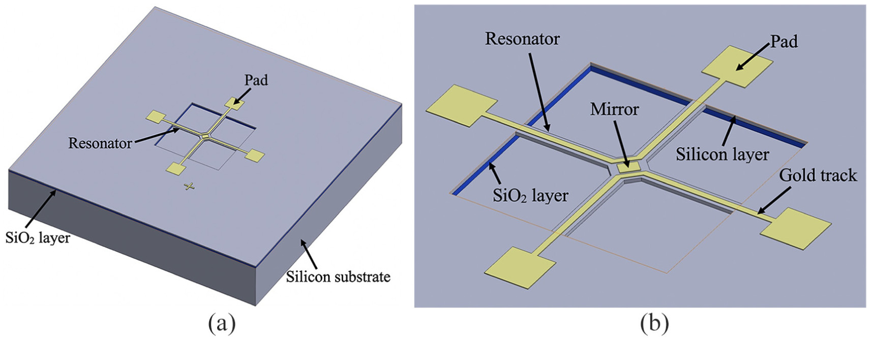
3D view of the design of a magnetic field sensor based on (a) silicon resonator that is composed of (b) two orthogonal silicon beams, two gold tracks, and a mirror.
Two sinusoidal electrical currents (IAu) flow through gold tracks under an in-plane magnetic field, as shown in Figure 2(a) and (b). This interaction causes a Lorentz force (FL) perpendicular to the resonator surface, allowing the vibration at its first bending resonant frequency. FL is determined by


where L is the length of each silicon beam, IRMS is the root mean square (RMS) of the electrical current IAu, f is the frequency, and t is the time.
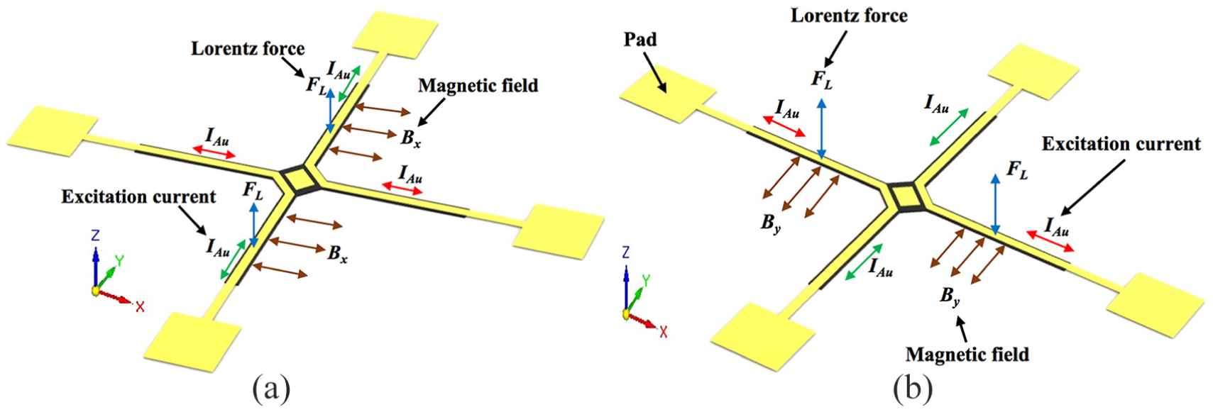
Operation principle of the magnetic field sensor under components of magnetic field along the (a) x-axis and (b) y-axis directions.
The displacements of the resonator mirror caused by in-plane magnetic fields can be detected using an optical system. The sensitivity of the sensor is determined as

where Δz is the displacement shift of the mirror and ΔB is the variation of in-plane magnetic field.
Analytical modeling of the resonant frequency
This section presents the analytical modeling to estimate the first bending resonant frequency of the sensor structure, which considers the Macaulay and Rayleigh methods as well as Euler–Bernoulli beam theory.
The bending moments, reaction loads, and weight per unit length (ω1, ω2, and ω3) on the sensor structure are shown in Figure 3. By considering a symmetric structure, the bending moments and reaction loads in each clamped-end have equal magnitudes (Ma = Mb = Mc = Md = M0 and Fa = Fb = Fc =Fd = F0). For the analysis of the mechanical behavior, we considered the following assumptions: Euler–Bernoulli beam theory, sensor structure composed of homogeneous and isotropic materials, small deflections of the resonator, and the weights of the gold tracks and mirror are neglected. In addition, we regard equal weight per unit length (ω1 = ω3) for sections 1 and 3. The weight in each jth section is determined as

where g is the gravitational acceleration.
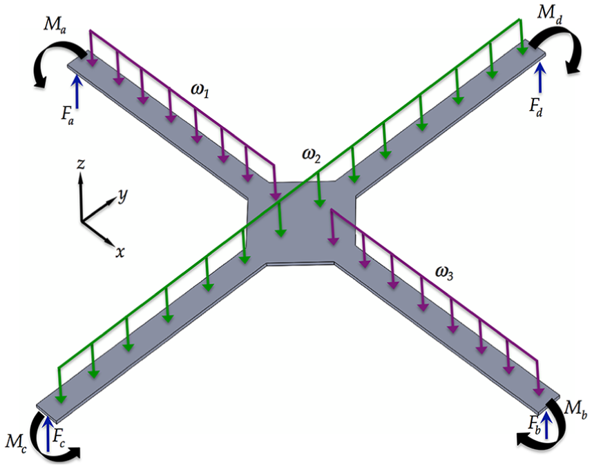
Schematic view of the reaction loads, bending moments, and uniformly distributed weights on the magnetic field sensor.
In order to simplify the analysis of the mechanical behavior of the sensor, its resonator (see Figure 4) is divided into three different sections with lengths of L1, L2, and L3. Thus, the maximum kinetic energy (Kmax) and the maximum potential energy (Pmax) of the resonator is calculated as


with

where Y and ρ are Young’s modulus and density of the resonator material, φ = 2πf, and zj(x), Ij, tj, and dj are the bending deflection, moment of inertia, thickness, and width in the jth section of the resonant structure, respectively.
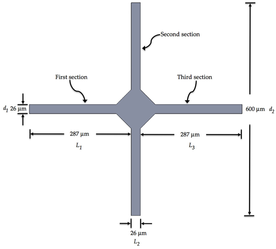
Dimensions of the silicon resonator of magnetic field sensor.
Using the Rayleigh method, the first bending resonant frequency (fr) of sensor is approximated as

Considering the Euler–Bernoulli theory, the bending deflections of the sensor structure are obtained as


where Mj(x) is the bending moment in the jth section of the sensor structure, which may be represented with Macaulay functions.
Deflections of the three sections of the sensor structure must satisfy the following boundary conditions

Using the Macaulay method,22,23 the bending moment functions (as given in Appendix 1) in each section of the sensor structure is calculated. Thus, the bending deflection zj(x) of each section of the resonator is determined using equations 9(a)–(c). For this, we use the bending moment functions, boundary conditions, and integration rules of Macaulay functions. For each section, the bending deflections of the sensor structure are expressed as
For

For
with


For

with

By substituting equations 11(a)–(c) into equations (5) and (6), we obtain the maximum potential and kinetic energies of the sensor structure. Next, these energies are substituted in equation (8) to estimate the first bending resonant frequency (fr) of the sensor structure. For this case, we assume the following parameters: ρ = 2330 kg m−3, Y = 169.8 GPa, t1 = t2 = t3 = 2 µm, d1 = d3 = 26 µm, d2 = 600 µm, L1 = L3 = 277 µm, and L2 = 26 µm. Based on equation (8), the fr = 43.84 kHz.
Damping sources
The resonator performance is affected by the damping sources, which limit its displacements. The principal sources of damping are air damping, thermoelastic damping, and support damping.
The damping level of a resonator is related with its total quality factor Qt, which measures the amount of energy loss of the resonator during its performance. The total quality factor is calculated using the ratio of the total energy stored in the resonator (Et) to the energy factor lost per cycle (El) due to the damping effect

The damping ratio (ζ) of the resonator is approximately equal to the reciprocal of twice the total quality factor24,25

For a double clamped beam, the quality factor (Qa) related with the air damping at atmospheric pressure can be estimated as26–28

where fr is the resonant frequency of the beam, ρ is the density of the silicon, t and d are the thickness and width of the beam, and η0 and ρ0 are the viscosity and density of the environment (air), respectively.
The thermoelastic damping is caused by the energy loss of the resonator due to irreversible heat conduction across strain-induced thermoelastic temperature gradients. 29 The bending motions of the silicon beams generate oscillating stress gradients across their thicknesses, which generate oscillating temperature gradients. These temperature gradients will lead to irreversible heat conduction, energy dissipation, and entropy generation. 30 For a thin beam, the quality factor (Qted) related with the thermoelastic damping can be expressed with the following analytical model 31

with

where α, κ, and Cp are the thermal expansion coefficient, thermal conductivity, and specific heat at constant pressure of the beam material, respectively; and T0 is the equilibrium temperature of the beam.
Support damping of a resonator depends of the vibration energy dissipated by transmission at its support. 32 The bending vibration of a resonator produces both vibrating moment and shear force on its clamped ends, exciting elastic waves through the resonator. An amount of this vibration energy is absorbed by the resonator supports. The quality factor (Qsup) due to the support damping for a double clamped beam is calculated as 32

where L and t are the length and thickness of the beam, respectively.
For our sensor design, the resonant structure is an array of two silicon orthogonal beams with a double clamped for each one. The total quality factor (Qt) of the proposed resonator is estimated as

where Qat = Qa/2 and Qsupt = Qsup/2.
Based on the first resonant frequency (fr = 43.84 kHz) estimated with analytical model, the total quality factor and damping ratio are approximated as 14.2 and 35.2 × 10⁻³, respectively.
Mirror displacements
This section regards the analytical modeling of the mirror displacements of the magnetic field sensor when it operates at resonance under magnetic field.
Figures 5 and 6 depict the displacements of a fixed-fixed beam caused by a magnetic field (By) with orthogonal direction (y-axis) to the length of the beam This By interacts with a sinusoidal excitation current (IAu) to generate two Lorentz forces (FL) in z-axis direction in each side of the beam along x-axis, which generates mirror displacements (zm) in z-axis direction. Assuming small displacements of the silicon doubly clamped beam, the displacement (zm1s) at the half of its length in static condition (without resonance) due to one concentrated load (FL) is approximated by 33

where L is the length of the fixed-fixed beam.
Schematic 3D view of the deflection of the resonator caused by two Lorentz forces (FL) due to the interaction of a magnetic field (By) and an electrical current (IAu).

Schematic 2D view of the deflection of a doubly clamped beam of the resonator caused by two Lorentz forces (FL).
Based on equation (19) and considering two concentrated loads (FL) of Figure 6 as well as the superposition method, the total displacement (zm2s = 2zm21s) at the half of the beam length in static condition is given by

When the doubly clamped beam is at resonance, its dynamic displacement is Qt times its static displacement. 34 Thus, the dynamic displacements of the mirror, located at the half of the beam length, are estimated as

Due to the symmetrical design of the resonator, two Lorentz forces (FL) in z-axis direction in each side of the second doubly clamped beam are obtained when a magnetic field (Bx) is applied in x-axis direction (see Figure 2(a)). For this case, the dynamic displacements of the mirror are also determined by equation (21). Thus, the proposed sensor can detect orthogonal magnetic fields (Bx and By) through the measurements of the mirror displacements using an optical system.
Fabrication
The magnetic field sensor is fabricated using a 4-in silicon-on-insulator (SOI) wafer with <100> orientation which has an active silicon layer of 2 µm thickness over a buried silicon oxide of 2 µm thickness and 450 µm of silicon substrate. Standard bulk micromachining process was employed to fabricate the sensor at the clean room facilities of CREOL, The College of Optic and Photonics at the University of Central Florida (CREOL-UCF).
The fabrication process starts by thoroughly cleaning the wafer with alcohols (acetone, methanol, and isopropanol) (Figure 7(a)). Next, the wafer surface is coated with negative photoresist (NR7-1000PY from Futurrex) as a continuous layer using a spin coater (4000 r/min for 40 s) and baked at 150°C on a hotplate for 60 s (Figure 7(b)). After this, the first photolithographic process defines the gold pads and tracks (Figure 8(a)). This process requires the irradiation of the water at a constant intensity of 12 mW/cm2 using a mask aligner (Karl-SUSS MJB3) with an exposure time of 12 s, and followed by a post-exposure bake at 100°C by 60 s. The wafer is developed using the resist developer RD-6 during 8 s and then the wafer is rinsed with deionized water (Figure 7(c)). Later, the gold pads and tracks are defined using chromium (5 nm thickness) and gold (110 nm thickness) layers, which are deposited in a thermal evaporator (Edwards Auto 306) (Figure 7(d)). The following stage is an annealing process using a rapid thermal annealing (RTA) at 250°C for 300 s to improve adhesion of the metal layers to the active silicon surface (Figure 7(e)).

(a)–(p) Fabrication process steps for the MEMS magnetic field sensor.

Patterns of negative mask used in the fabrication: (a) gold pads and tracks and (b) resonator beams.
The resonator beams are defined as follows. First, a silicon dioxide layer (∼200 nm) is deposited using plasma-enhanced chemical vapor deposition (PECVD) in a Plasma-Therm 790 RIE/PECVD system (Figure 7(f)). Next, negative photoresist NR7-1000PY is spin coated (4000 r/min for 40 s) and baked at 150°C for 60 s (Figure 7(g)). A second photolithographic process similar to the first one is used to define the regions (Figure 8(b)), where a metal hard mask will be evaporated to create the resonator beams (Figure 7(h)). The hard mask is formed by evaporating 180–200 nm of chromium using the thermal evaporator (Figure 7(i)) and a lift-off process with RR2 at 120°C for 5–10 min is used to remove the chromium that is not making contact with the silicon dioxide, thus defining the metal mask (Figure 7(j)). Next, the silicon active layer and the SiO2 layer are dry-etched (Plasma-Therm 790 RIE/PECVD) during 23 and 20 min, respectively (Figure 7(k)). After the dry etching, the remaining chromium film is removed using a standard chromium wet-etching process for 10 min (Figure 7(l)) and the remaining 200 nm of silicon dioxide is eliminated through a commercial 1:6 buffered oxide etch (BOE) for 4 min (Figure 7(m)).
In order to release the resonator beams, the following procedure is employed. We first cover with SU-8 photoresist (1 µm thickness) the gold tracks and pads, using standard photolithographic SU-8 process (Figure 7(n)), to protect them from the chemical process in the next step. The resonator is released using a wet-etching process using BOE during 1 h (Figure 7(o)). Finally, SU-8 is removed through oxygen plasma for 20 min (Figure 7(p)). Finally, the magnetic field sensor is packaged in a DIP-20 (20-pin dual in-line package). Figure 9 shows scanning electron microscopy (SEM) images of the resonant silicon beams, gold tracks, and mirror of the magnetic field sensor.

SEM images of a magnetic field sensor composed of a (a) silicon resonator and (b) gold tracks and mirror.
Results and discussion
After the fabrication process, the packaged sensor is tested to measure its experimental resonance frequency. Figure 10 shows the experimental setup to measure the resonance frequency of the magnetic field sensor. In this setup, the cavity between the tip of the single-mode optical fiber and the micromirror of the sensor was 10 μm. It was verified that the reflection was good, and then we read the output values. The value of the wavelength of the tunable laser was set to 1495 or 1509 nm, because at these wavelengths the measurement was better with respect to the cavity. The minimum laser power was 700 μW and the magnetic field source was 20 mT. The sine-wave alternating current was supplied to the sensor through a function generator with a value of 12 mA. This current flowed to a single gold loop of the resonant structure and a frequency sweep was made. A photodetector measured the sensor response (see Figure 11), obtaining a resonance close to 53 kHz.

Schematic view of the optical reading system proposed to measure the output signal of the magnetic field sensor.

Experimental resonance frequency of the magnetic field sensor.
In the fabrication process, there were cases in which the sensor structure was not released due to stiction problems. A test was carried out with a frequency of approximately 2.5 Hz in the sinusoidal alternating current. This current was supplied by the function generator to the gold loop of the sensor and without applied magnetic field. We observed the sensor motion due to heating Joule effect. If the structure showed a out-of-plane motion, then it was completely released. With an oscilloscope, we measured (see Figure 12(a) and (b)) the sinusoidal electrical current (above signal) supplied to the sensor and its output voltage (below signal). In Figure 12(a), the sensor presents variable output voltages due to its oscillating motion. This indicates that the sensor structure was suitably released. However, Figure 12(b) shows a non-variable output voltage of another magnetic field sensor whose structure was not completely released.
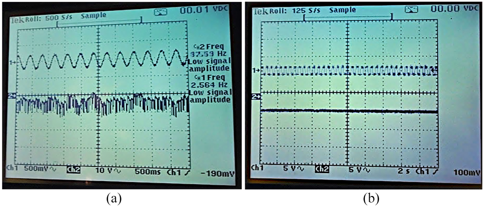
Output voltage of a magnetic field sensor: (a) with released structure and (b) without released structure. A sinusoidal alternating current of 2.5 Hz was supplied to the gold loop of the sensor.
We developed finite element method (FEM) models of the resonator through ANSYS® software to predict its mechanical response. These FEM models employ solid95 and solid227 type elements and regard four fixed supports at the ends of the resonator. In addition, FEM models take into account the silicon beams and gold tracks, whose materials properties are shown in Table 1. To simply the calculations, we modeled the silicon considering Young’s modulus (Ex = Ey) of 169 GPa and Poisson’s ratio (vxy) of 0.064, which are theoretical values of the [110] direction within silicon (100) plane. Figure 13 depicts the first bending vibration mode of the sensor structure, which has a frequency of 45.6 kHz. This frequency value has a relative difference of 4.0% and 14.0% respect to those obtained with the Rayleigh method and experimental setup, respectively. This bending vibration mode is suitable for the sensor operation, since it will allow an out-of-plane motion (z-axis direction) of the mirror. Figure 14(a)–(d) depicts the second, third, fourth, and fifth vibration modes of the resonator. These vibration modes are not suitable for resonator operation, since they do not have modal shapes with out-of-plane bending. Therefore, these vibration modes do not enable out-of-plane motions (z-axis direction) of the mirror.
Properties of the materials used in FEM models of magnetic field sensor.

FEM: finite element method.
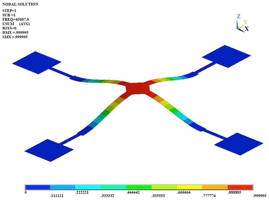
First vibration mode (45.6 kHz) of the resonator of magnetic field sensor.
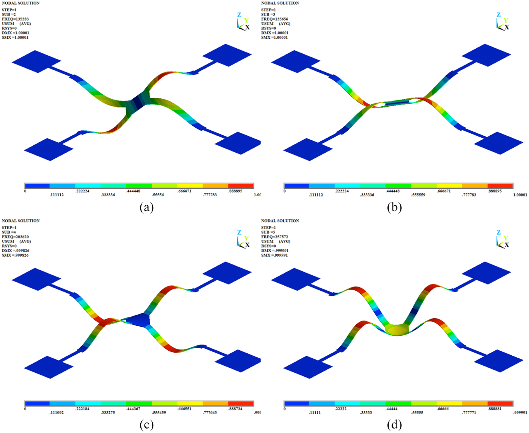
(a) Second (135.28 kHz), (b) third (135.66 kHz), (c) fourth (203.62 kHz), and (d) fifth vibration mode (257.57 kHz) of the resonator of magnetic field sensor.
After the modal analysis, the mechanical behavior of the sensor structure at resonance (45.6 kHz) is studied considering a magnetic field range from 1000 to 10,000 µT and three different values for IRMS (10, 20, and 30 mA). To avoid the electromigration failure of the gold tracks, we consider a maximum current density of 2 × 10¹⁰ A m−2,35–37 supplied to these tracks. Thus, the maximum electrical current flowing into the gold tracks must be less than 35.2 mA. After, we determine the out-of-plane displacements of the sensor mirror, as shown in Figure 15. These results are compared respect to those of the analytical model of equation (21). For both models, the mirror displacements have a linear behavior for the applied magnetic field. The mirror displacements of the FEM model agree well with those of the analytical model, achieving a relative difference of 13.8%. This difference is because the analytical model does not consider the stiffness of the second doubly clamped beam, which decreases the total stiffness of the resonator and increases the total displacement of the mirror. In addition, FEM models include two materials of the resonator (silicon beam and gold tracks), increasing the total stiffness of the resonator. For a magnetic field of 10,000 µT and IRMS = 30 mA, the mirror has a displacement of 395.8 nm, as shown in Figure 16. Based on the results of the FEM models and using three values IRMS (10, 20, and 30 mA), the sensitivities of the sensor are 13.2, 26.4, and 39.6 µm T−1, respectively. On the other hand, the sensor sensitivities considering the analytical displacements have magnitudes of 15.4, 30.7, and 46.1 µm T−1, respectively. The linear response of the sensor is suitable for monitoring magnetic field with a simple optical system. Also, values of the three principal stresses of the resonator do not overcome the rupture stress of the silicon beam (1 GPa), as shown in Figure 17(a)–(c). The absolute values of the maximum magnitudes of the three principal stresses are 14.8, 15.1, and 21.1 MPa, respectively. Thus, the performance of the sensor will be safe for magnetic field less than 10,000 µT. Assuming IRMS of 10, 20, and 30 mA flowing through gold track (measured resistance of 60 Ω), the magnitudes of the power consumption are 6, 24, and 54 mW, respectively. Thus, this sensor can detect in-plane magnetic fields with a low consumption power, linear response, and safe performance.

Out-of-plane displacements (nm) of the mirror of magnetic field sensor obtained using analytical and FEM models.

Out-of-plane displacement (µm) of the resonant structure of magnetic field sensor caused by a magnetic field of 10,000 µT and IRMS of 30 mA.
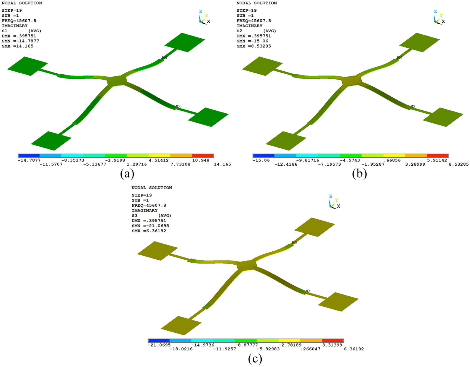
(a) First, (b) second, and (c) third principal stresses of the resonating magnetic field sensor under IRMS = 30 mA and magnetic field By = 10,000 µT.
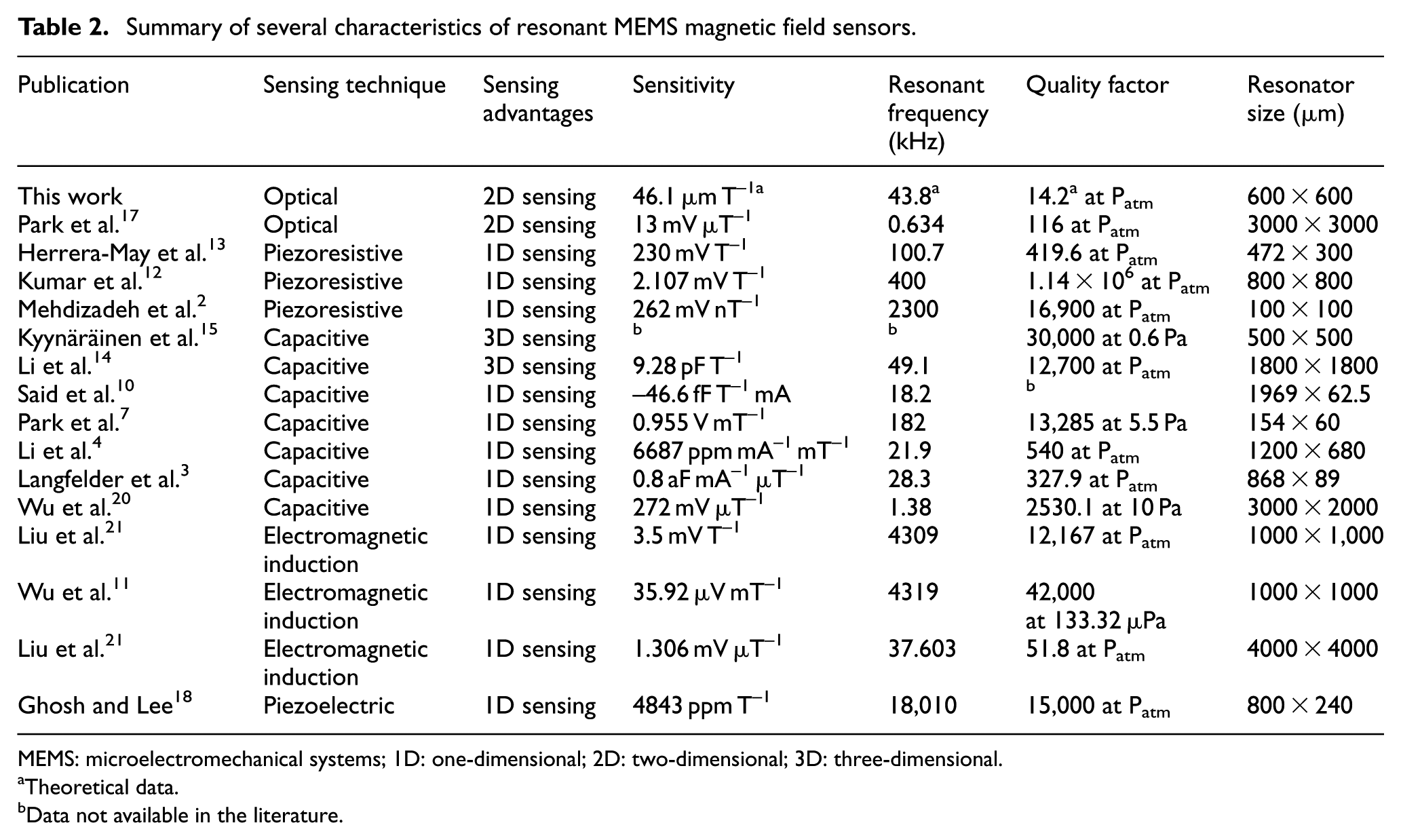
Table 2 shows a comparison of performance characteristics of several resonant MEMS magnetic field sensors. Most of these sensors can only detect magnetic field along a single axial direction, which limits their applications. However, our magnetic field sensor can detect in-plane magnetic field using a simple resonant structure and optical sensing technique. The proposed sensor has a small size and low bending resonant frequency in comparison with other sensors.
Summary of several characteristics of resonant MEMS magnetic field sensors.
MEMS: microelectromechanical systems; 1D: one-dimensional; 2D: two-dimensional; 3D: three-dimensional.
Theoretical data.
Data not available in the literature.
In order to detect the mirror displacements using a compact system, we propose the design of a portable optical system included in two printed circuit boards (PCBs), as shown in Figure 18. The bottom PCB will contain the magnetic field sensor, a regulator, a battery, and a current source. The upper PCB will keep a regulator, a silicon NPN phototransistor, a peripheral interface controller (PIC 16F84A), a vertical cavity surface emitting laser (VCSEL), and a liquid crystal display (LCD). In this system, the electrical current will be generated by the current source with an electronic oscillator. This current will supply the gold tracks with a frequency equal to the first resonant frequency of the magnetic field sensor. On the other hand, the regulators will hold constant voltages in the current source, phototransitor, VCSEL, PIC controller, and electronic oscillator. Thus, when the electrical current interacts with an orthogonal magnetic field to the resonator, then the generated Lorentz force will cause out-of-plane displacements of the mirror, which will be measured through VCSEL and phototransistor. In these measurements, VCSEL will emit infrared wavelength light on the sensor mirror, which will be reflected to phototransistor. It will transmit output voltage signals to PIC 16F84A, whose values will be function of the mirror displacements and applied magnetic field. Thus, the magnetic field signals will be converted to output voltage signals using the magnetic field sensor with the proposed optical system.
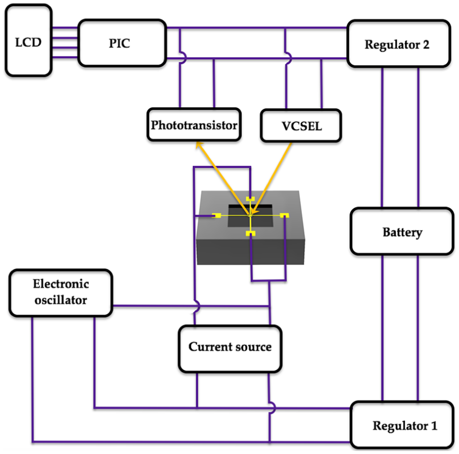
Schematic view of the proposed optical system for the magnetic field sensor.
Conclusion
A magnetic field sensor based on a silicon resonator and an integrated gold mirror is designed and fabricated using a SOI wafer in a bulk micromachining process. The resonator is composed by two fixed-fixed beams with gold tracks and a mirror. This resonator is operated at resonance under in-plane magnetic fields and sinusoidal electrical currents. Thus, the applied magnetic field generated out-of-plane displacements of the mirror, which registered a linear behavior. Analytical models are developed to determine the first bending resonant frequency, quality factor, and out-of-plane displacements of the resonator. In addition, FEM models are implemented to obtain the first vibration modes, displacements, and stresses of the sensor resonator. The mechanical response of the sensor determined with analytical models agreed well with those of the FEM models. The sensor had a safe mechanical performance for a magnetic field range from 1000 to 10,000 µT, achieving stress values less than the rupture stress of the silicon (1 GPa). For three different electrical currents IRMS (10, 20, and 30 mA), the sensor reached analytical sensitivities of 15.4, 30.7, and 46.1 µm T−1, respectively. The sensor registered an experimental resonant frequency of 53 kHz. A portable optical system was proposed to detect the out-of-plane displacements of the mirror related with the applied magnetic field.
For future work, we will optimize the resonator performance, considering mirror folded beams. In addition, we will study the resonator displacements at both bending and torsional modes.
Footnotes
Appendix 1
The function of the shear load V(x) of the sensor structure is determined integrating equation (22) and using the integration rules of Macaulay functions. 22 The function of the bending moment M(x) of the sensor structure can be obtained integrating twice equation (22). Thus, M(x) is represented by
where D1 and D2 are constants that are calculated through the values of the shear load (V(0) = F0) and bending moment (M(0) = M0) at fixed ends of the resonator. For this case, we calculated D1 = D2 = 0.
For each section of the resonator, the bending moment functions are obtained through equation (23).
For
For
For
Acknowledgements
The work was partially supported by projects PRODEP “Estudio de Dispositivos Electrónicos y Electromecánicos con Potencial Aplicación en Fisiología y Optoelectrónica” and PFCE 2019 “DES Técnica Veracruz 30MSU0940B-405.”
Handling Editor: Min Zhang
Declaration of conflicting interests
The author(s) declared no potential conflicts of interest with respect to the research, authorship, and/or publication of this article.
Funding
The author(s) received no financial support for the research, authorship, and/or publication of this article.