
Abstract
A fast and intelligent defect classification system for distinguishing defect features is developed in this study. Defect images obtained from an automated optical inspection instrument are first trained utilizing a deep learning approach based on the convolutional neural network. The detailed features of defects, such as flaws in the inclination, size, quantity, and settlement, can then be characterized with the developed system. The obtained defect characteristics can be provided as a reference to evaluate the manufacturing process. A graphics processing unit card is used to build the parallel computing architecture for fast data computation both in the training and classification processes. The experimental results show that the defect classification for a touch panel glass surface of size 43 × 229.4 mm2 that yields 805 million pixel data points was completed in 2 s. The classification accuracy was above 96%. Therefore, an automated and fast defect analysis catalog integrated to an optical inspection result for the evaluation and adjustment of manufacturing operations can be expected with the proposed approach.
Keywords
Introduction
Automated optical inspection (AOI) equipment has been widely used for real-time detection of defects and quality control of products on the production line.1–3 Artificial neural networks have also been applied to these AOI systems to improve the accuracy of defect inspection.4–6 Although the introduction of artificial intelligence (AI) enhances the speed and accuracy for defect detection, an effective advice for evaluation and improvement of the manufacturing process from the inspected results is still a problem until now. The main difficulty is that the inspection can only check the existence of defects but cannot recognize the details of defect features such as the inclination and size of flaws. Therefore, there is a high demand for building an intelligent defect classification system to evaluate the production status from the measured surface features and defects of products.
With the development of AI technology, some feature-based defect classification algorithms were proposed.7,8 With the help of the AI-assisted classification system, a manufacturing control mechanism for real-time visualization, analysis, and management may be implemented in association with the information of image detection, various statistical data, and design parameters in each production line. However, these defect classification approaches based on classic neural networks and classifiers mainly rely on the programmer or user to specify the feature characteristics without the ability of self-learning and self-improvement.9,10
Recently, deep machine learning technique was gradually induced into AOI systems to improve the accuracy of defect detection.11,12 As it was known, the technology of deep learning is very powerful. A major advantage of machine learning is that the model can learn from past predictions and results, and continually improve their predictions based on new and different data. 13 Therefore, through the continuous learning process, we can not only determine whether there is a flaw in the detection process but also simultaneously quantify the various characteristics of defects, such as flaws in the inclination, size, quantity, and settlement. An automated defect evaluation system can then be established and combined with process parameters to provide suggestions for the improvement of the manufacturing process. The evaluation-based approach will not only improve the overall production throughput in every manufacturing line but also expand the industrial chain with a more intelligent decision.
In this study, an artificial neural network based on the deep learning method with convolutional technique 14 was constructed for defect classification and evaluation. The characteristics of defect features were learned and continuously improved from the network itself. A graphics processing unit (GPU) card was utilized to deal with large data for fast data computation. 15 The inspection was performed on the surface of a touch panel glass with an area of 43 × 229.4 mm2 that yields 16,115 test images, each 224 × 224 pixels in size. The total time for the classification can be completed within 2 s using the GPU card. The accuracy of classification was from 96% to 100%. This shows that a higher classification speed and accuracy was achieved. The classification results can efficiently provide more information in the detected images and may be used to evaluate the test samples and put forward the influencing factors of the manufacturing process.
Neural network architecture
The architecture of the deep learning network adopted in this study is shown in Figure 1. A ZF-Net neural model 14 contains seven learning layers—five convolutional layers and two fully connected layers were adopted to perform the training and evaluation of defect images. The first convolutional layer filters a 224 × 224 crop from an image of 256 × 256 by 96 kernels of size 7 × 7, using a stride of 2 in both the x and y directions. The resulting feature is activated through a rectified linear function ReLU(x) = max(x, 0) and pooled by taking maximum local neighborhoods within each 3 × 3 region with a stride of 2. The output is then taken as the input of the second layer and the similar operations are repeated in layers 2–5. Layers 6 and 7 are fully connected, taking features from the last convolutional layer by 16 kernels as input in vector form as 16 × 256 = 4096 dimensions. The classification result of the ZF-Net model is expressed with a C-way softmax function, where C is the number of classes.

Architecture of the neural network model.
The input images are obtained from an optical inspection system as shown in Figure 2. A linear charge-coupled device (CCD) camera (Basler raL12288–66 km) with 12,288 pixels and 3.5 μm per pixel resolution is used to construct the imaging module. Lighting is provided by two sets of light-emitting diode (LED) arrays located on both sides of the lens assembly, respectively, illuminating the specimen at a lower angle to form a typical dark-field illumination. As the specimen translates with the stage, light scattered from the surface of the specimen due to surface defects is collected by the linear CCD. When the surface is smooth and flawless, light is completely reflected and refracted from the surface without entering the CCD, producing a full black background image. A GPU operation card (NVIDIA GeForce® GTX 1080) is used to build the parallel computing architecture for fast data computation both in the training and classification processes.

Schematic of the inspection system.
The flowchart for defect classification and characterization is shown in Figure 3. First, images grabbed by the linear CCD are processed to flatten the intensity distribution of the raw image. The normalization is executed for all pixels and the outputs are stored in the allocated memory after equalization. As mentioned, the training and classification processes of the recorded defect images are processed with the ZF-Net learning algorithms. The network is initialized by setting up all its weights as random numbers. The constants of learning rate (η) and momentum (α) are also assigned to approximate that of a ReLU activation function. After choosing the weights W00, …, Wij, and a bias (Θ) for each initial picture map, the ReLU function would compute for each input and the necessary corrections are simultaneously completed in the output pattern.
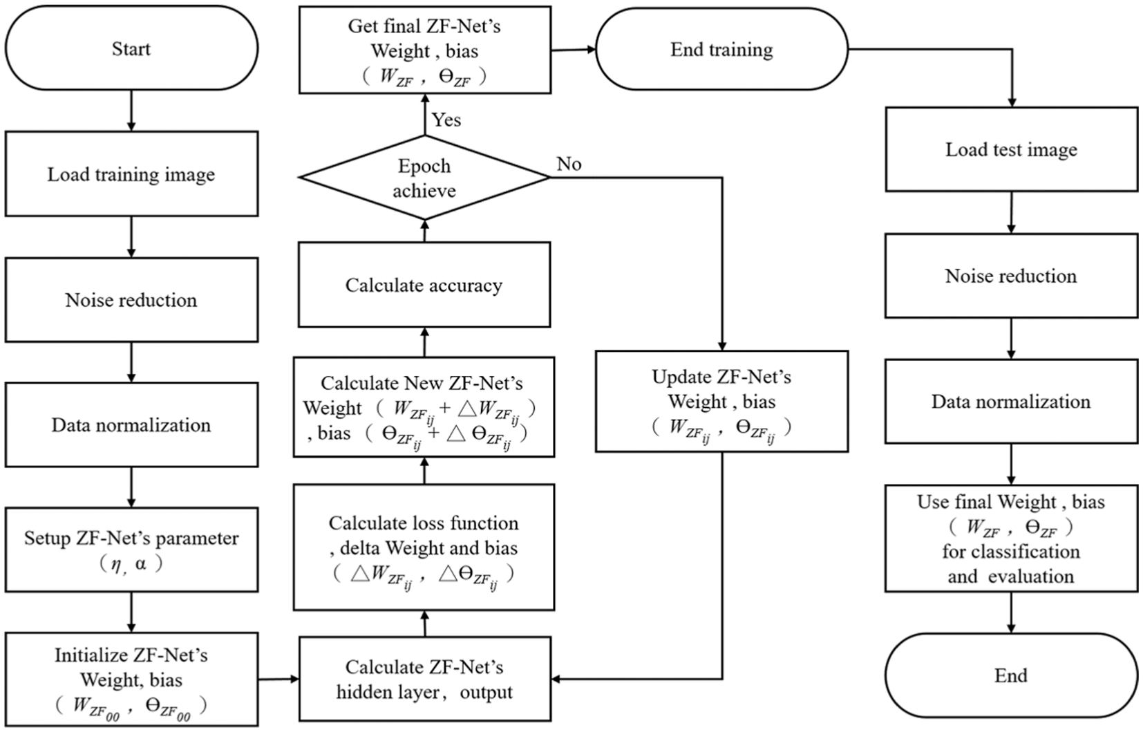
Operation flowchart for defect classification and characterization.
Since all the initial weights and biases are random, the calculation returns an output that is completely different from the target. To quantify the deviation from the target the algorithm computes for the error, which represents the difference between the target and the actual outputs. Here, backpropagation or backward passes to the output and hidden layers calculate the change in weights and biases until such that the output is very close to the target. The loss function sparse_categorical_cross_entropy between the new weights for each successive iteration cycle is calculated and then the weights are updated as Wij (updated) = Wij + △Wij and Θij (updated) = Θij + △Θij. Once the loss value becomes sufficiently small and the set cycle time is completed, the updated weights and biases are used as the final weights and biases for the following classification of the test images.
Training process
The training patterns used in this study are currently limited to defect features that are found in touch panel glass and back-coated mirror according to the manufacturer. The defects consist of surface scratches and bubble features, which can be attributed to improper processing. These defect images were grabbed with a 10-kHz line rate. A total of 100 image pictures with representative defect patterns and a fixed window size of 256 × 256 pixels from the actual inspection results were first chosen in the training process. Five images with a size of 224 × 224 pixels were randomly selected from each of the 100 defect pictures. Each of the 500 images was rotated 90° gradually to obtain four sets of images and their mirror images, resulting in a total of 4000 training samples to execute the training process of deep learning with GTX 1080. The training parameters including the learning rate, momentum, bias, and training cycles are shown in Table 1.
Parameter values for training process in the neural network.

In order to make the defect detection results to provide more details and characteristics of these defects, which may be used as a reference for the manufacturer to improve the process, this study defined 11 categories of defect items as shown in Table 2. The corresponding images and meanings for each category are shown in Figure 4. When the number of defects in an image is greater than 3, the image is defined as multiple defects, otherwise it is defined as few defects. When the length of a scratch is greater than 40 pixels, the scratch is defined as long scratch; otherwise, it is defined as short scratch. When the diameter of a bubble is greater than 15 pixels, the bubble is defined as large bubble; otherwise, it is a small bubble. The inclination of a scratch is determined by its tilt angle. When the tilt angle is greater than 20° either in the vertical or horizontal direction, it is a tilt defect.
Category of defect classification.


Defect category items and their respective meanings.
Before these defect types are trained by ZF-Net neural model, we need to manually specify the defect image attribution for all 4000 training samples. Figure 5 shows the process for some examples of these chosen images. Each image is first confirmed for which items of defect category it contains. According to the characteristics of each image, a set of labels containing 11 categories is given for this image. The categories appearing in this image are labeled 1 and the rest are marked as 0. The image is then trained in each category labeled 1.
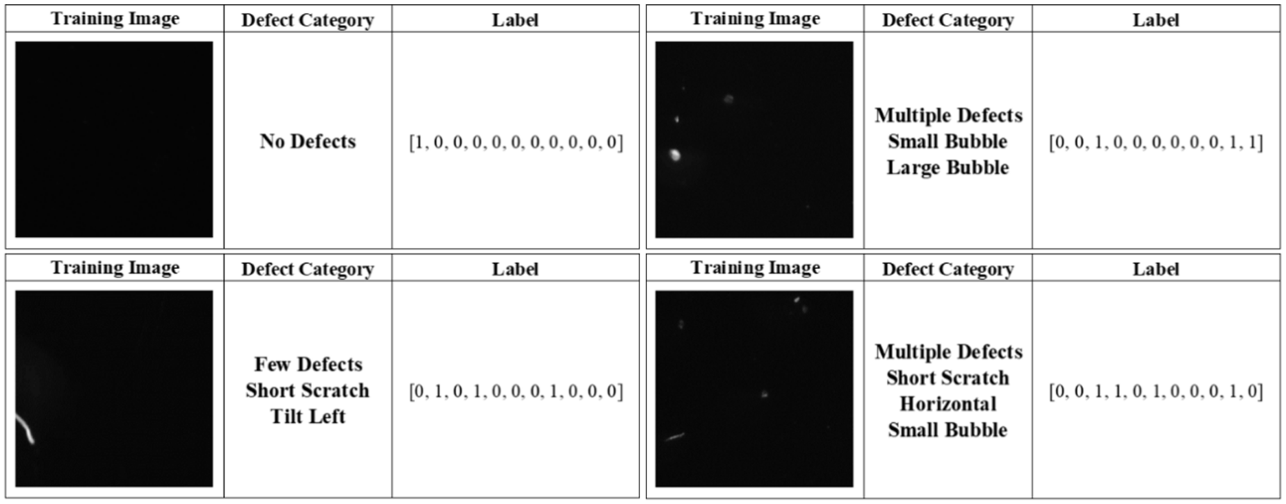
Defect category and label for training samples.
Test results and discussion
Defect inspection and classification experiments were first carried out on the surface of a touch panel glass. The magnification of imaging CCD was set to 1×. So its measurement width for the linear CCD was roughly 43 mm. A surface with an area of about 43 × 229.4 mm2 was inspected, which generated 12,288 × 65,536 ∼805 megapixel image data. Thus, a total of 16,115 images, each with a size of 224 × 224 pixels were tested for defect classification. Since a 10-kHz line rate of the linear CCD was adopted in the AOI system, the scan time for 65,536 imaging lines was nearly 7 s. However, experiments showed that the classification process of the 16,115 images can be completed within 2 s using GTX 1080. Some typical test results are shown in Figure 6, where the output was expressed with the probability of occurrence for each category of defect. The category with a percentage below 10% is currently considered as noise or minor issue and is not included in the output items. The determination of the threshold value is dependent on the user. A total of 1000 test images were randomly taken to visually confirm their classification accuracy. Inspection results showed that the defect belonging to scratch or bubble can be 100% identified but the accuracy of characterizing the inclination of defects was roughly 96%. This may be caused by some of the defects that are inclined toward nearly 20°, so that they are not easy to exactly judge which category they belong to.

Defect classification output for test images.
The second object to be tested was a back-coated mirror. The width and length of the scratch found on the sample was about 10–20 μm and 1–10 mm, respectively. Point-like defects ranging from 50 to 160 μm in diameter were also observed and seen as bubbles. Since the resulting dark-field images are very similar to those obtained from touch panel glass, the resulting classification speed and accuracy are also consistent.
The use of varied training samples in size, shape, and orientation by ZF-Net neutral network has been verified to be capable of improving the classification outcome of the actual test samples by showing more details of the various defect features. In fact, the defect category and output details can be determined by the user according to the adopted items in the training process. Even using dozens of or hundreds of classifications is theoretically feasible. In addition, if information about the manufacturing parameters can be obtained in advance, more evaluations between these classification details and processing parameters can be done by combining an additional neutral network system. The output can even be adjusted with the adjustment of processing parameters via simulation results. Therefore, this presented approach can be an effective tool to provide references for improvement of the manufacturing process.
Conclusion
An intelligent defect inspection and classification system based on deep learning algorithm has been developed. The artificial network system was constructed with ZF-Net neural model to perform defect image training and evaluation. A GPU card was utilized to deal with large data for fast data computation. Experimental results showed that a total of 16,115 images each with a size of 224 × 224 pixels were processed in 2 s. The classification accuracy was above 96%. This indicates that the defect category and feature details can be quickly and effectively characterized with the proposed approach. The current category items are limited to 11 characteristics of surface scratches and bubble features that are found on glass and mirror surfaces. However, it is possible to carry out more classifications for multiple defects on various products by further training the algorithm to catalog different defect types and their feature details. Thus, with the proposed system, it is possible to streamline the relationship between defect category and manufacturing parameters for improvement of the process in production lines.
Footnotes
Handling Editor: Wen-Hsiang Hsieh
Declaration of conflicting interests
The author(s) declared no potential conflicts of interest with respect to the research, authorship, and/or publication of this article.
Funding
The author(s) disclosed receipt of the following financial support for the research, authorship, and/or publication of this article: This research was financially supported by the National Natural Science Foundation of China under Grant Nos 51605171 and 51505162. It was also supported by Research Foundation for Advanced Talents of Huaqiao University (Grant No. 16BS504) and the Open Project of Key Laboratory of Modern Precision Measurement and Laser NDT in Fujian Province (Grant No. 2016XKA001).