
Abstract
Thin-film transistor liquid crystal display surface micro-defects are difficult to be detected using traditional threshold or edge detection methods. This article puts forward a non-destructive detection method using particle swarm optimization with one-class support vector machine to inspect thin-film transistor liquid crystal display surface micro-defects. An image acquisition system is constructed to acquire the surface micro-defects images of thin-film transistor liquid crystal display. Background textures are removed by the image preprocessing algorithm based on one-dimensional discrete Fourier transform. Moreover, the wavelet transform algorithm is used to eliminate the influence of uneven illumination. Effective characteristic parameters describing thin-film transistor liquid crystal display surface micro-defects are selected by the principal component analysis method. Classification model is developed based on one-class support vector machine using radial basis function. To validate the method above, other parameter optimization algorithms, including normal algorithm, genetic algorithm, and grid search algorithm, are used to optimize the support vector machine model parameters: penalty parameter C and kernel parameter g. In contrast, particle swarm optimization is proved to get the optimal model parameter, and the recognition accuracy of 91.7% is obtained from the particle swarm optimization–one-class support vector machine model. The results indicate the proposed system and method can accurately inspect thin-film transistor liquid crystal display surface detects.
Keywords
Introduction
Thin-film transistor liquid crystal displays (TFT-LCDs) are widely used in televisions, notebook computers, mobile phones, and other electronic products because of the advantages of power saving, thin and low radiation, space saving, and so on. However, TFT-LCD surface defects have plagued the image quality of TFT-LCD, and surface defect detection of TFT-LCD has become one of the key technologies of TFT-LCD production.
There are three basic methods for inspecting TFT-LCD surface defects: artificial visual inspection method, electrical parameter detection method, and automatic visual inspection method. 1 Affected by the reasons of subjectivity, slow speed, poor stability, and others, manual visual inspection is difficult to meet the needs of large-scale production. Electrical parameter detection method is limited to detect electrical defects. Automated optical inspection (AOI) method is to obtain the TFT-LCD surface image by machine vision system and inspect defects by image processing method. AOI is the inevitable trend of the TFT-LCD surface defects detection and classification because of its high accuracy, high speed, and non-contact detection, which has become the focus of many research scholars.2,3
According to the size of TFT-LCD surface defects, they can be divided into macro defects and micro-defects. 4 Macro defects are relatively large and can be identified by naked eyes. Mura is the common macro defect, and there are many experimental results on it. 5 However, micro-defects are relatively small and cannot be identified by naked eyes or common electrical parameter method. As been well known, micro-defects can be divided into pinholes defects, scratch defects, and particle defects.
The AOI process of TFT-LCD surface defects detection mainly involves three aspects: image preprocessing, image segmentation, and defects classification. Image preprocessing and segmentation belong to the category of digital image processing, and they are traditional methods and relatively mature. Defects classification belongs to the category of pattern recognition, and the statistical learning theories are introduced into the automatic classification of surface defects, which play a very important role in TFT-LCD automation production.
The methods of TFT-LCD surface defects recognition mainly include neural network classifiers, support vector machines (SVMs), dynamic Bayesian networks, and so on. These algorithms have been widely used in TFT-LCD surface defects. Neural network method improves the recognition rate by providing adequate training samples in training process, but it has the disadvantages of weak generalization ability and longer training time and can easily lead to overfitting because of a small or unrepresentative training set. SVM is derived from the theory of statistical learning theory (SLT) by Vapnik, 6 which is designed for pattern classification and regression estimation.7–9 SVMs have many advantages in generalization ability, global optimization, and so on compared with the traditional pattern classification and machine learning methods such as artificial neural networks and get more and more widely used. SVM has become an effective tool for TFT-LCD surface defect detection and classification, and domestic and foreign scholars have done many researches on it.10–13
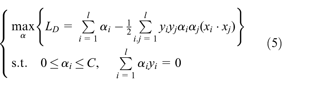
SVM is mainly to solve the problem of binary classification. In order to achieve the classification goal, the training sets need to include positive and negative sample points. However, the number of training samples of different defects is often very unbalanced in the actual defect detection process. If we still use the classification method, the classification accuracy is low. For solving this problem, the defect detection method based on one-class support vector machine (OCSVM) is proposed, which only determines whether the sample has a defect and providing a true or false result.
In our work, a non-destructive detection method using particle swarm optimization (PSO) with OCSVM is proposed to inspect TFT-LCD surface micro-defects. The feasibility of classification is considered in this proposed system.
System construction and testing process
TFT-LCD surface defect detection system mainly consists of the following components: linear Charge Coupled Device (CCD) camera, optic lens, light source, image acquisition unit, image processing software, and related components. The schematic diagram is shown in Figure 1. DALSA’s linear CCD camera (Piranha ES80-04k-40 with 8192 pixels and 7.4 µm × 7.4 µm pixel size) was used in the TFT-LCD surface defect detection system. The diameter of TFT-LCD surface defect is less than 1 mm, and the required measurement resolution is about 15 µm. The aperture lens of SIGMA’s with 105 mm focal length and F2.8 aperture can meet the resolution requirements of defect detection. Halogen linear light source is used. Camera support bracket and light source support bracket can be adjusted, and the stage moves at constant speed on the rails drove by motor. The images of TFT-LCD surface defects are collected by CCD camera, transferred to, and stored in a computer by image acquisition card.

Structure block diagram of TFT-LCD surface detection system.
The detection process of TFT-LCD surface defects is shown in Figure 2. First, TFT-LCD surface image is collected by the CCD industrial camera; then, the image noise is filtered out by image preprocessing and the defective area is divided; finally, the defect feature information is extracted for the classification of TFT-LCD surface defects; and the recognition results are given.

Flowchart of TFT-LCD defect detection.
Image processing
Image preprocessing
Horizontal gate line and vertical data line are arranged regularly in TFT-LCD. Thin-film transistor (TFT) is located at the intersection of gate line and data line. Periodic background texture seen in the TFT-LCD image is the part of TFT. The scanned images of three kinds of TFT-LCD surface micro-defects (pinholes, scratches, and particles) are shown in Figure 3. They all have periodic textured background.

TFT-LCD surface micro-defects: (a) pinholes, (b) scratches, and (c) particles.
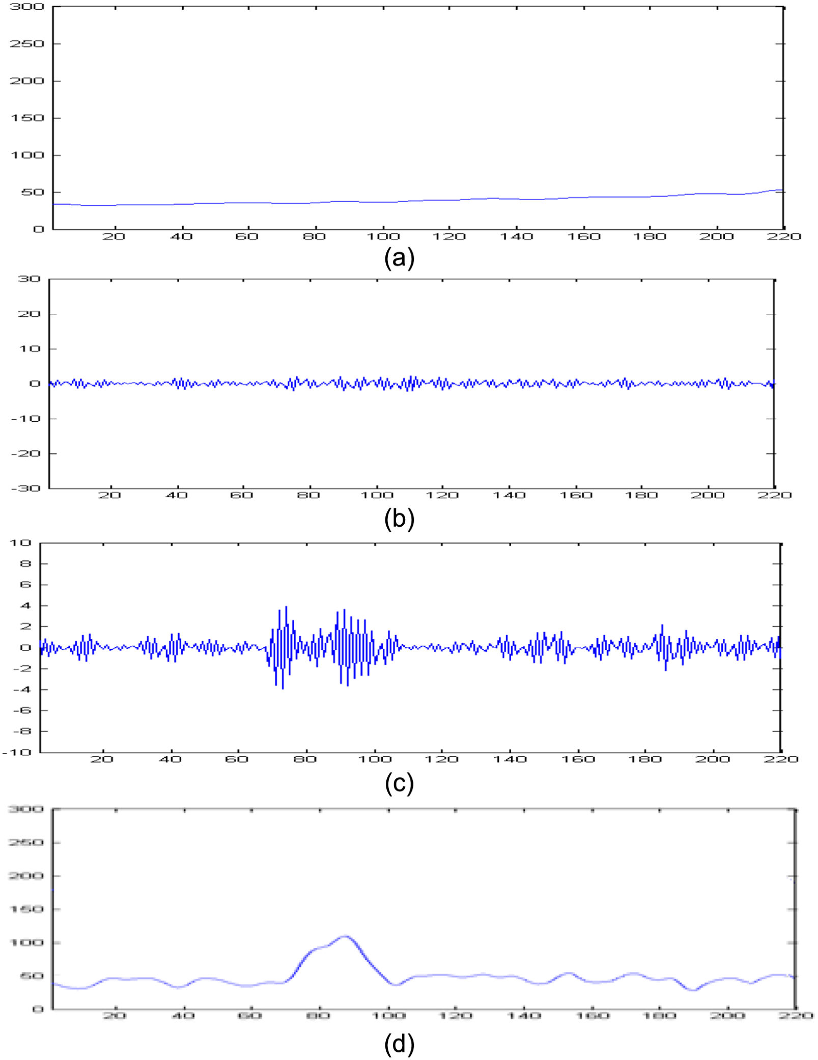
Figure 4(a) is the gray-scale image of defect-free line scan in Figure 3(a). As shown, the peak position is located at the liquid crystal array. In the scan imaging process, the uneven illumination of light source will result in the uneven distribution of gray peak height, but this will not cause peaks mutation. Figure 4(b) is the gray-scale image of pinhole defect line scan in Figure 3(a). The pinhole defect leads to the mutation of image gray peak, which can determine the location of a TFT-LCD surface defect.

The line scan gray-scale image and its reconstruction of liquid crystal array: (a) the gray-scale image of defect-free line scan, (b) the gray-scale image of pinhole defect line scan, (c) the reconstructed image of (a), and (d) the reconstructed image of (b).
The defect image information processing in periodic texture surface is more complex than in uniform surface, because the texture background needs to be eliminated and retained the defect information. Frequency filtering method is a common method of periodic texture filtering. Images are filtered by frequency domain transform, such as Fourier transform (FT), 14 discrete cosine transform (DCT),15,16 wavelet transform (WT), 17 Gabor wavelet transform (GWT), 18 and so on. First, the frequency components of repetitive texture background are eliminated in frequency domain analysis; then, the image is reconstructed by corresponding inverse transform; finally, the image without repeating textured background is obtained.
In this article, the images of TFT-LCD surface defects are obtained through linear CCD camera by line scanning. To ensure the real-time system requirements, one-dimensional (1D) discrete Fourier transform (DFT) is adopted to remove the textured background; then, the image without repeating textured background is obtained the inverse discrete Fourier transform (IDFT); finally, the defects are detected by defect recognition and classification algorithm. The abnormal fluctuations of high-frequency component of 1D signal processed by IDFT are eliminated by head and tail splicing method. Figure 4(c) and (d) is the gray distribution image reconstructed through 1D DFT and head and tail splicing. Because the gray distributions are uneven in Figure 4(c) and (d), the defects cannot be directly detected by thresholding method; otherwise, the normal is mistaken for defect. This article proposes a WT method to detect defects.
In the below equations,
Here,
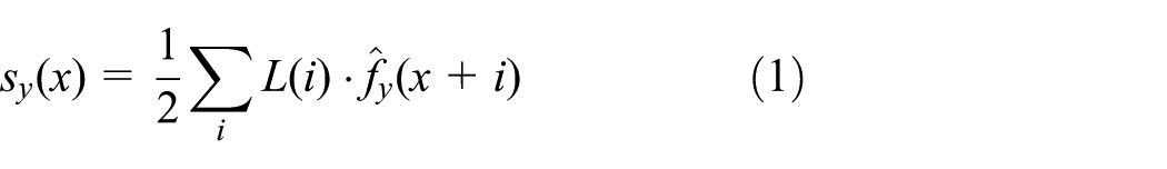
Figure 4(c) and (d) is transformed into Figure 5 by 1D Haar WT. Figure 5(a) and (c) is the smooth dimensional image
The results of one-dimensional Haar wavelet transform (WT): (a) sy(x) of Figure 4(c), (b) dy(x) of Figure 4(c), (c) sy(x) of Figure 4(d), and (d) dy(x) of Figure 4(d).
Defect feature extraction
The defect features of TFT-LCD surface micro-defects are extracted after segmentation and edge detection of the TFT-LCD surface defect image. The image features mainly include five feature sets: geometry feature, shape feature, first-order statistical moments feature, second-order statistical moments feature, and moment invariants. Geometry feature set contains central location, direction, perimeter and area, and so on. Shape feature mainly describes the outer boundary and the overall shape of the region. First-order statistical moments describe the gray distribution of defects. Second-order statistical moments describe the texture feature of defects. Moment invariants have the invariance characteristics of rotation, translation, and scaling.
The shape feature has a great relationship with the size or location of defects, so it cannot be directly used as the feature of defect classification. The best features of defects classification should be independent of position, shape, and deflection angle. In order to ensure the validity of feature information, reduce the calculation amount, and improve the processing speed, the principal component analysis (PCA) is used to extract features.
There are mainly three types of TFT-LCD surface micro-defects: pinholes, scratches, and particles. The characteristics of defect types are described by 20 feature values extracted, such as area, perimeter, roundness, flatness, duty cycle, the minimum bounding rectangle (MBR), aspect ratio, gray-scale range, mean gray, gray variance, gray energy entropy, first-order moments feature, second-order moments feature, and Hu moment invariants, which constitute the feature space of TFT-LCD surface micro-defects.
The complexity of recognition grows rapidly with the increase in dimensions because the characteristic values are relevant. PCA method is used to extract the main component characteristic parameters from the 20 dimensionality features in order to reduce dimensionality and redundant data. According to the standard of cumulative contribution ratio of the principal component reaching 90%, five principal component characteristic parameters are retained, which constitute the feature subspace of TFT-LCD surface micro-defects. In order to facilitate subsequent processing, the characteristic parameters must be optimized and normalized.
Defect classification algorithm
SVM principle and pattern recognition
TFT-LCD panel defect classification is actually a pattern recognition category. SVM19–21 is a machine learning method proposed by Vapnik based on the SLT and structural risk minimization, which is different from the traditional method based on the empirical risk minimum (ERM) principle. SVM with high generalization capability has more advantage in solving the problem of small sample, nonlinear, and high-dimensional recognition.
The basic idea of SVM is to map the input samples from low-dimensional feature space to the high-dimensional feature space by kernel functions and establish the optimal classification surface in the high-dimensional feature space. Assuming that the sample collection is
Through the normalized processing, the samples closest to classification interface meet
Here, C is the classification error penalty factor. The problem of linear constrained quadratic programming is solved using Lagrange’s optimization method, that is

Here,
In dealing with the nonlinear classification problem, the input samples of SVM are mapped from the original space to a high-dimensional feature space through nonlinear mapping function
OCSVM
In the process of surface defect classification, sometimes some new types of defects occur and need to be classified, but the number of defect samples of the new types is small and is not balanced compared with the number of training defect samples of other types. In this case, the normal SVM classification method will reduce the classification accuracy.
Along with thorough research and an urgent need for engineering application, some new algorithms about SVM are constantly found out, such as least squares support vector machine (LS-SVM), 22 fuzzy SVM, 23 OCSVM,24,25 and multi-class support vector machine (MSVM).26,27
OCSVM was originally proposed for outlier detection, which was regarded as one-class classification for solving the quadratic programming problem. OCSVM has effectively solved the problem of high dimension, local minima, and nonlinear classification. Tax and colleagues25,28,29 proposed a support vector data description (SVDD) classifier, which was realized by constructing the hypersphere method. B Schölkopf et al.24,30 presented OCSVM classification algorithm, which was realized by constructing the hyperplane separated from the origin. OCSVM has been widely used in fault diagnosis, network intrusion detection, target recognition, and so on.31–33
The basic idea of OCSVM is to describe the objects as a whole, to construct a closed and compact area, and to make the described object be included in the region as much as possible. Given the training sample points sets
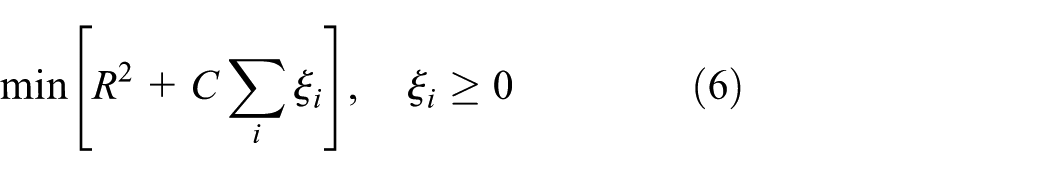
where C is penalty factor which plays the role of controlling the punishment degree of error-classifying samples to achieve a compromise between the proportional extent error-classifying samples and the complexity of algorithms. According to the Lagrange’s multiplier method

Here,

A new sample of z is determined whether it belongs to the target sample by the following formula

If the formula (9) is satisfied, it is determined that z belongs to the target sample, otherwise it is judged to be a non-target sample and refused. Radius R can be determined by calculating the distance z to a support vector
Kernel parameter optimization based on particle swarm algorithm
Kernel functions, as the key of SVM method, mainly contain the polynomial kernel function, radial basis function (RBF) kernel function, and sigmoid kernel function. The selection of kernel function does not have determined method and specific theoretical basis. Vapnik et al. 34 have proved that in the above three kinds of kernel functions, regardless of the sample size or the dimension level, RBF kernel functions are all applicable.
RBF kernel function has strong self-learning and self-regulation ability, and it is an ideal classification function. Therefore, this study employs an RBF kernel function in the SVM to classify TFT-LCD surface defect samples. The RBF is as follows
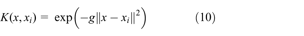
OCSVM is modeled based on RBF kernel function. The model has two main parameters: the penalty factor C and the kernel parameter g. To get a good SVM classifier, the key is to select and optimize the value of nuclear parameters C and g. Parameter C is used to achieve a compromise between model complexity and misclassification ratio. If the C value is too large, it will lead to the reduction in SVM generalization ability. On the contrary, if the value is too small, it would affect the classification results. Parameter g represents the width of the kernel function, which plays an important role in improving the performance of SVM classification.
The common parameter optimization algorithms35–38 include genetic algorithm (GA), grid search algorithm (GSA), and so on. These algorithms when dealing with high-dimensional complex problems will easily fall into local extreme accuracy and low defects. However, when the algorithms are used to deal with complex high-dimensional optimization problems, they can easily cause the problems of local extrema and low accuracy. To solve this problem, PSO algorithm is selected to optimize and determine the parameters.
PSO, developed by Professors Kennedy and Eberhart, 39 is an efficient parallel optimization algorithm based on swarm intelligence, which is originated from the predatory behavioral research of birds. PSO is a global search algorithm based on iterative update, which searches for the optimal solution through collaboration and information sharing among and between individuals. 40 Because of the advantages of parameter-less and fast convergence, it has been widely applied in function optimization, pattern recognition, and so on.41–43 Its principle can be described below.
Assume that the population consists of m particles. A particle is seen as a point in D dimensional space, which represents the solution of the problem and its status is described by its position and speed. In D dimensional space, the position vector and velocity vector of the
The velocity and position of each particle are updated by formula (11)

Here,
Penalty parameter C and kernel parameter g are optimized by PSO and OCSVM. The flowchart of the algorithm is shown in Figure 6:
Step 1. Set up the search range of SVM model and PSO parameters (population size, learning factors, inertia weight, maximum number of iterations, and maximum speed).
Step 2. The values of C and g generated randomly are used as the initial position of each particle. Initialize the velocity and position of all particles randomly.
Step 3. Initialize the individual optimal and global optimal locations of particles and calculate individual fitness value of the population. Compare individual fitness value with local optimal solution and global optimal solution. According to the comparison results, update local optimal solution and global optimal solution.
Step 4. Update velocity and position of all particles according to the results of step 3.
Step 5. If the maximum number of iterations is reached, return the optimal solution and terminate optimization; otherwise, continue to implement Step 3.

The flowchart of optimization parameters of PSO-OCSVM algorithm.
Experimental results and analysis
In total, 60 samples are prepared for each type of defect images (pinholes, scratches, and particles). For each type, 40 samples are extracted as the training set by random sample generation method, and the rest 20 samples are used as the test sample set.
For OCSVM classification model, the search range of penalty factor C is [0.0001, 100]; and the search range of kernel parameter g is [0.0001, 100]. For PSO algorithm, the learning factor is c1 = c2 = 2, the maximum number of iterations is 50, the number of particles dimension is 2, the maximum velocity is 1, the maximum inertia weight is 0.9, and the minimum inertia weight is 0.3.
In order to evaluate the performance of the classification method, GA, GSA, and PSO are also used to optimize the SVM model parameters: kernel parameter g and penalty parameter C. Five principal component characteristic parameters are selected as the model input parameters. Table 1 is the classification results of TFT-LCD micro defect test samples based on these algorithms. The following can be drawn from the table:
The highest accuracy rate is 91.7%, which caused mainly by two reasons. On the one hand, the classification accuracy rate of micro-defects is relatively lower than macro defects’. On the other hand, the illumination has a certain influence on the feature extraction of defect area and causes some false positives and false negatives, such as broken line and hole shadow.
The performance of parameter optimization algorithm is better than the normal algorithm (kernel parameter g and penalty parameter C are randomly selected). The accurate recognition rate of normal algorithm is only 80%. PSO algorithm is proved to get the optimal model parameter (C = 64.637 and g = 0.359), and the recognition accuracy of 91.7% is obtained.
PSO-OCSVM with excellent performance and high reliability can be applied to the classification of TFT-LCD surface micro-defects.
Results of OCSVM model based on different parameter optimization methods.

OCSVM: one-class support vector machine; PSO: particle swarm optimization; GA: genetic algorithm.
Conclusion
The rapid detection method of TFT-LCD surface micro-defects is proposed based on PSO and OCSVM. An image acquisition system is constructed to acquire the surface micro-defects images of TFT-LCD. Background textures are removed by 1D DFT. WT algorithm is used to eliminate the influence of uneven illumination. Effective characteristic parameters describing TFT-LCD surface micro-defects are selected by PCA. Prediction model is developed based on OCSVM using RBF. By comparing with the algorithms of normal, GA, GSA, and PSO, PSO algorithm is proved to get the optimal model parameter (C = 64.637 and g = 0.359), and the recognition accuracy of 91.7% is obtained. The results indicate that the proposed TFT-LCD surface defect detection system and the PSO-OCSVM method can be used to inspect micro-defects with high classification accuracy.
Footnotes
Academic Editor: Gang Chen
Declaration of conflicting interests
The author(s) declared no potential conflicts of interest with respect to the research, authorship, and/or publication of this article.
Funding
The author(s) disclosed receipt of the following financial support for the research, authorship, and/or publication of this article: This research was supported by a grant from the National Key Scientific Instrument and Equipment Development Projects, China (2013YQ220749), Key Project of Science and Technology Research of Henan Province Education Department, China (16A510028), the National Natural Science Foundation of China (U1304305).